

Philips tda9847 DATASHEETS

INTEGRATED CIRCUITS
DATA SH EET
TDA9847
TV and VTR stereo/dual sound
processor with digital identification
Preliminary specification
Supersedes data of September 1993
File under Integrated Circuits, IC02
1995 May 23

Philips Semiconductors Preliminary specification
TV and VTR stereo/dual sound processor
TDA9847
with digital identification
FEATURES
• Supply voltage 5 to 8 V
• Source selector
• Stereo matrix
• AF inputs for external stereo AF signals
(SCART or NICAM)
• AF outputs for main and SCART
• LED operation mode indication (stereo and dual)
• High identification reliability.
QUICK REFERENCE DATA
SYMBOL PARAMETER CONDITIONS MIN. TYP. MAX. UNIT
V
I
P
V
P
i(rms)
supply voltage (pin 22) 4.5 5 8.8 V
supply current (pin 22) without LED current 14 15 20 mA
nominal input signal voltage
54% modulation
Vi1to Vi4 (RMS value)
V
o(rms)
nominal output signal voltage
54% modulation − 500 − mV
(RMS value)
V
o(rms)
clipping level of the output signal
THD ≤ 1.5%; B/G or L
voltages (RMS value)
I
V
Lon
i pil
input current LED on −−12 mA
input voltage sensitivity of pilot
unmodulated 5 − 100 mV
frequency
S/N(W) weighted signal-to-noise ratio
“CCIR468-3”
THD total harmonic distortion − 0.2 0.3 %
T
f
ident
amb
operating ambient temperature 0 − +70 °C
identification window width stereo 2.2 − 2.2 Hz
dual 2.3 − 2.3 Hz
t
ident on
V
i tuner
∆f
pil
total identification time on 0.35 − 2.0 s
identification voltage sensitivity − 28 − dBµV
pull-in frequency range of pilot PLL f
osc
GENERAL DESCRIPTION
The TDA9847 is a stereo/dual sound processor for TV and
VTR sets. Its identification ensures safe operation by using
internal digital PLL technique with extremely small
bandwidth, synchronous detection and digital integration
(switching time maximum 2.0 s; identification concerning
the main functions).
B/G − 250 − mV
L − 500 − mV
= 5 V 1.4 1.60 − V
V
P
= 8 V 2.4 2.65 − V
V
P
66 75 − dB
= 10.008 MHz
lower side −296 −−296 Hz
upper side 302 − 302 Hz
ORDERING INFORMATION
TYPE
NUMBER
NAME DESCRIPTION VERSION
TDA9847 SDIP24 plastic shrink dual in-line package; 24 leads (400 mil) SOT234-1
TDA9847T SO24 plastic small outline package; 24 leads; body width 7.5 mm SOT137-1
1995 May 23 2
PACKAGE
Philips Semiconductors Preliminary specification
TV and VTR stereo/dual sound processor
with digital identification
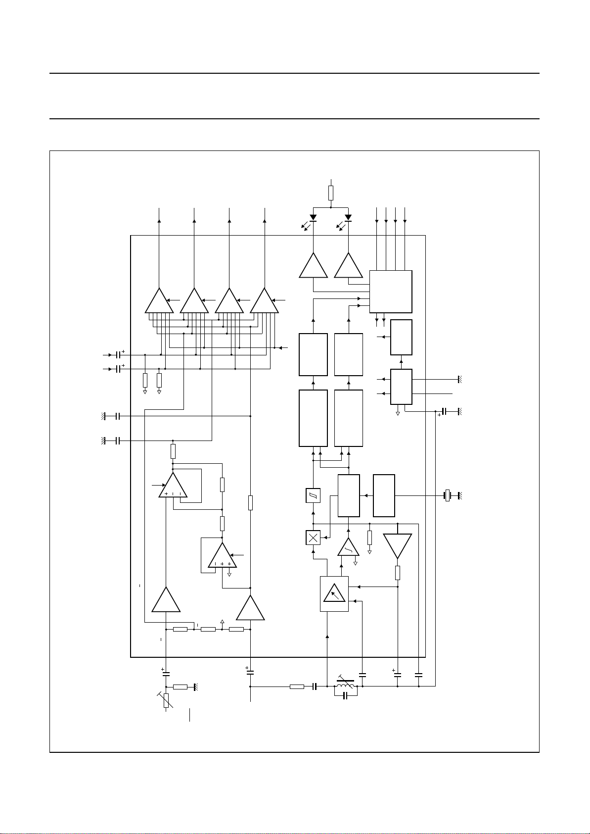
BLOCK DIAGRAMS
i3
V
i4
SCART
V
250 mV
250 mV RMS
RMS
±5%
10 nF
D2
C
D1
C
±5%
10 nF
2.2 µF 2.2 µF
17 21 12 11
o1
V
14
500 mV RMS
6 dB
50 kΩ
refVref
V
50 kΩ
5 kΩ
main
V
RMS
AM
250 mV
o2
13
500 mV RMS
6 dB
L/A/mono
o3
V
16
500 mV RMS
6 dB
RMS250 mV
L
SCART
o4
V
15
500 mV RMS
R/B
250 mV RMS
6 dB
V
1 kΩ
stereo transmission
19
dual bit
(274 Hz)
mute
DIGITAL
INTEGRATOR
AND
DIGITAL PLL
DEMODULATOR
P
18
bit
stereo
DIGITAL
AND
DIGITAL PLL
C1C2C3
dual transmission
1
2
(117 Hz)
INTEGRATOR
DEMODULATOR
C4
3
24
LOGIC
CONTROL
RESET
POWER-ON
SUPPLY
ref
V
202223 8
MED803
P
1/2 V
P
V
ref
C
100 µF/
16 V
TDA9847
A/mono
5 kΩ
6 dB (AM)
2.2 µF
2.2 kΩ
0 dB
3 dB
3 dB
9
V
10 kΩ 10 kΩ
ref
V
ref
0 dB
V
3 dB
15 kΩ
35 kΩ
50 kΩ
10
2.2 kΩ
, A
2
i1
L + R
250 mV RMS
(AM: 500 mV RMS)
V
TDA9847
2.2 µF
R, B
i2
250 mV RMS
1995 May 23 3
PLL
DIGITAL
7
= 70
o
2.5 mH
Q
47 pF
30 kΩ
FP
FP
R
C
3.3 nF
tan δ ≤ 0.002
V
ref
6
C
25 kΩ
DCL
ref
V
100 nF
OSCILLATOR
25 kΩ
4
10 µF
AGC
C
10 MHz
Fig.1 Block diagram of the bipolar TV/VTR-stereo decoder.
5
10 nF
LP
C
Input and output levels are nominal values related to the SCART norm (AM: m =0.54, FM: ∆f=±27 kHz).
Philips Semiconductors Preliminary specification
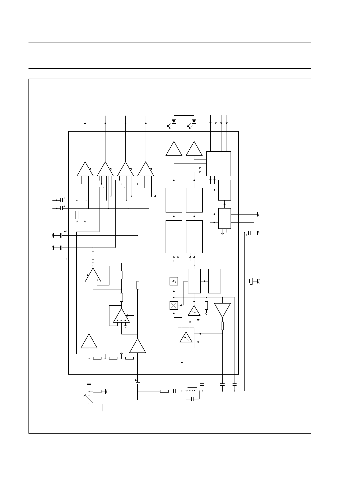
TV and VTR stereo/dual sound processor
with digital identification
i3
V
i4
SCART
V
250 mV
250 mV RMS
RMS
5%
10 nF
D2
C
D1
C
5%
10 nF
2.2 µF 2.2 µF
17 21 12 11
o1
V
14
500 mV RMS
6 dB
50 kΩ
refVref
V
50 kΩ
5 kΩ
main
V
RMS
AM
250 mV
o2
13
500 mV RMS
6 dB
L/A/mono
o3
V
16
500 mV RMS
6 dB
RMS250 mV
L
SCART
o4
V
15
500 mV RMS
R/B
250 mV RMS
stereo transmission
19
6 dB
dual bit
mute
DIGITAL
INTEGRATOR
AND
DIGITAL PLL
P
V
1 kΩ
18
bit
stereo
(274 Hz)
DEMODULATOR
(117 Hz)
DIGITAL
INTEGRATOR
AND
DIGITAL PLL
DEMODULATOR
C1C2C3
dual transmission
1
2
24
LOGIC
CONTROL
POWER-ON
V
C4
3
RESET
SUPPLY
ref
202223 8
MED804
P
1/2 V
TDA9847
P
V
ref
C
100 µF/
16 V
A/mono
5 kΩ
6 dB (AM)
2.2 µF
2.2 kΩ
0 dB
3 dB
3 dB
9
V
10 kΩ 10 kΩ
ref
V
ref
0 dB
V
3 dB
15 kΩ
35 kΩ
50 kΩ
10
2.2 kΩ
, A
2
i1
L + R
250 mV RMS
(AM: 500 mV RMS)
V
2.2 µF
R, B
i2
TDA9847
250 mV RMS
27 kΩ
FP
R
1995 May 23 4
180 pF
FP
C
7
±5%
4.7 mH
1.8 nF
PLL
DIGITAL
ref
V
6
= 25
o
Q
±2%
tan δ ≤ 0.01
C
25 kΩ
V
DCL
OSCILLATOR
ref
100 nF
10 MHz
25 kΩ
Fig.2 Block diagram of the bipolar TV/VTR-stereo decoder with fixed coil (alignment-free).
5
4
10 nF
10 µF
LP
C
AGC
C
Input and output levels are nominal values related to the SCART norm (AM: m = 0.54, FM: ∆f=±27 kHz).
The components of the external LC band-pass filter have the following order-No.: Philips Germany only No: 4312 020 17525 or Fastron Sdn. Bha., Malaysia type SMCC 472 J
for L = 4.7 MHz (±5%) Philips Components No: 2222 429 71802, C = 1.8 nF (±2%).
Philips Semiconductors Preliminary specification
TV and VTR stereo/dual sound processor
with digital identification
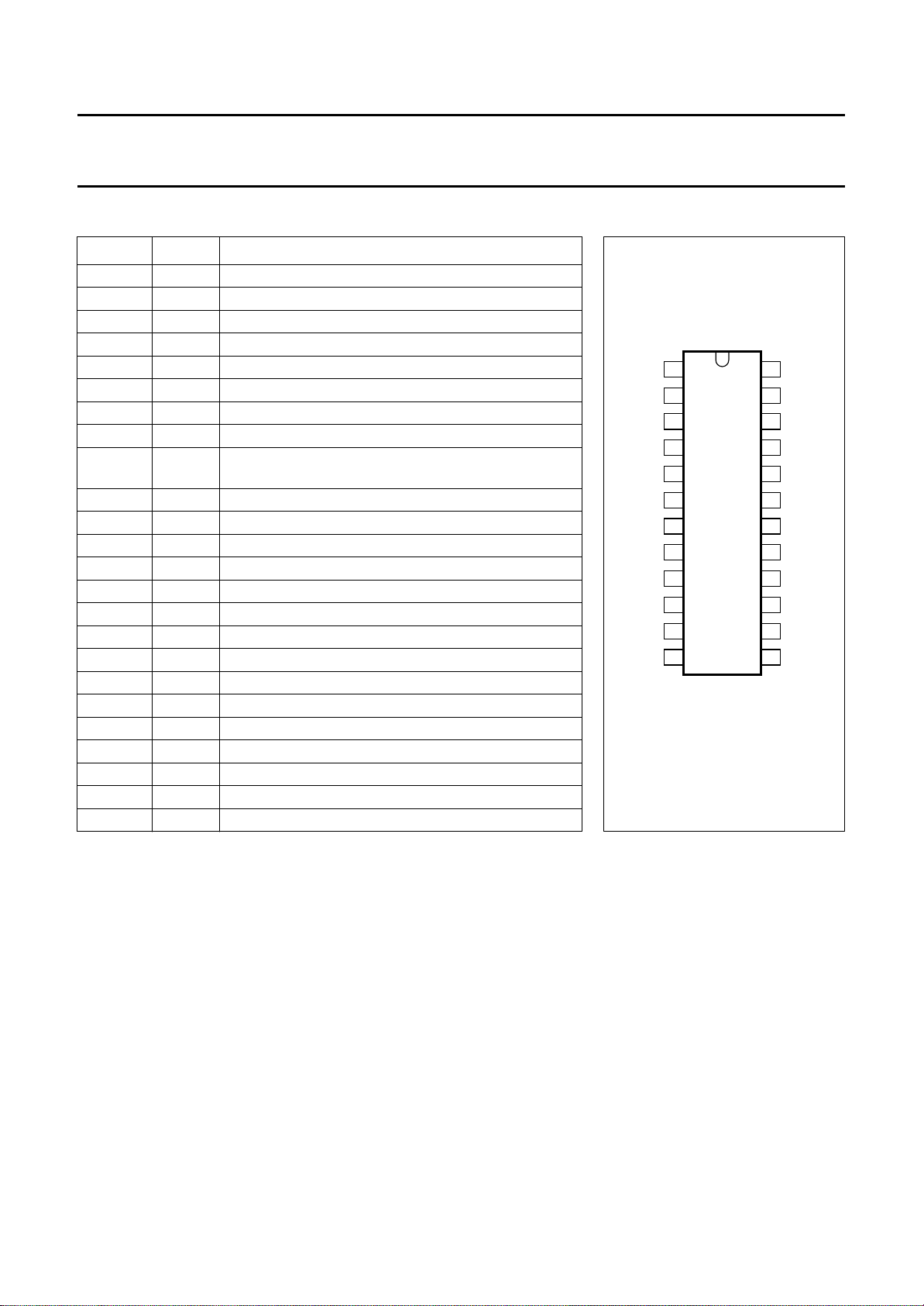
PINNING
SYMBOL PIN DESCRIPTION
C1 1 control input Port C1
C2 2 control input Port C2
C4 3 control input Port C4
C
AGC
C
LP
C
DCL
V
i pil
C
ref
V
i1
V
i2
V
i3
V
i4
V
o2
V
o1
V
o4
V
o3
C
D1
LEDDU 18 LED (dual)
LEDST 19 LED (stereo)
GND 20 ground (0 V)
C
D2
V
P
XTAL 23 10 MHz crystal input
C3 24 control input Port C3
4 AGC capacitor of pilot frequency amplifier
5 identification low-pass capacitor
6 DC loop capacitor
7 pilot frequency input voltage
8 capacitor of reference voltage (1⁄2VP)
9 AF input signal voltage 1 [from sound carrier 1 or
AM sound (standard L)]
10 AF input signal voltage 2 (from sound carrier 2)
11 AF input signal voltage 3 (SCART)
12 AF input signal voltage 4 (SCART)
13 AF output signal voltage 2 (main)
14 AF output signal voltage 1 (main)
15 AF output signal voltage 4 (SCART)
16 AF output signal voltage 3 (SCART)
17 50 µs de-emphasis capacitor of AF Channel 1
21 50 µs de-emphasis capacitor of AF Channel 2
22 supply voltage (5 to 8 V)
TDA9847
1
C1
2
C2
3
C4
4
C
AGC
5
C
LP
6
C
DCL
V
i pil
C
ref
V
V
V
V
Fig.3 Pin configuration.
TDA9847
7
8
9
i1
10
i2
11
i3
12
i4
MED805
24
23
22
21
20
19
18
17
16
15
14
13
C3
XTAL
V
P
C
D2
GND
LEDST
LEDDU
C
D1
V
o3
V
o4
V
o1
V
o2
1995 May 23 5

Philips Semiconductors Preliminary specification
TV and VTR stereo/dual sound processor
with digital identification
FUNCTIONAL DESCRIPTION
AF signal handling
The input AF signals, derived from the two sound carriers,
are processed in analog form using operational amplifiers.
De-matrixing uses the technique of two amplifiers
processing the AF signals. Finally, a source selector
provides the facility to route the mono signal through to the
outputs (‘forced mono’).
De-emphasis is performed by two RC low-pass filter
networks with internal resistors and external capacitors.
This provides a frequency response with the tolerances
given in Fig.4.
A source selector, controlled via the control input ports
allows selection of the different modes of operation in
accordance with the transmitted signal. The device was
designed for a nominal input signal (FM: 54% modulation
is equivalent to ∆f=±27 kHz) of 250 mV RMS value (V
and Vi2) and for a nominal input signal (AM: m = 0.54) of
500 mV RMS value (Vi1), respectively 250 mV RMS (V
and Vi4). A nominal gain of 6 dB for Vi1 and Vi2 signals
(0 dB for Vi1signal (AM sound)) and 6 dB for Vi3 and V
signals is built-in. By using rail-to-rail operational
amplifiers, the clipping level (THD ≤ 1.5%) is 1.60 V RMS
for VP= 5 V and 2.65 V RMS for VP= 8 V at outputs
Vo1to Vo3 and Vo4. Care has been taken to minimize
switching plops. Also total harmonic distortion and random
noise are considerably reduced.
i1
i3
i4
TDA9847
to obtain the AGC voltage for controlling the gain of the
pilot signal amplifier.
The identification stages consist of two digital PLL circuits
with digital synchronous demodulation and digital
integrators to generate the stereo or dual sound
identification bits which can be indicated via LEDs.
A 10 MHz crystal oscillator provides the reference clock
frequency. The corresponding detection bandwidth is
larger than ±50 Hz for the pilot carrier signal, so that
-variations from the transmitter can be tracked in the
f
p
event of missing synchronization with the horizontal
frequency fH. However the detection bandwidth for the
identification signal is made small (±1 Hz) to reduce
mis-identification.
Figure 2 shows an example of the alignment-free f
band-pass filter. To achieve the required QL of around 12,
the Q0 at fp of the coil was chosen to be around 25
(effective Q0 including PCB influence). Using coils with
other Q0, the RC-network (RFP and CFP) has to be adapted
accordingly. It is assumed that the loss factor tan δ of the
resonance capacitor is ≤0.01 at fp.
Copper areas under the coil might influence the loaded Q
and have to be taken into account. Care has also to be
taken in environments with strong magnetic fields when
using coils without magnetic shielding.
Control input ports
p
Identification
The pilot signal is fed via an external RC high-pass filter
and single tuned LC band-pass filter to the input of a gain
controlled amplifier. The external LC band-pass filter in
combination with the external RC high-pass filter should
have a loaded Q-factor of approximately 40 to 50 to
ensure the highest identification sensitivity. By using a
fixed coil (±5%) to save the alignment (see Fig.2), a
Q-factor of approximately 12 is proposed. This may cause
a loss in sensitivity of approximately 2 to 3 dB. A digital
PLL circuit generates a reference carrier, which is
synchronized with the pilot carrier. This reference carrier
and the gain controlled pilot signal are fed to the
AM-synchronous demodulator. The demodulator detects
the identification signal, which is fed through a low-pass
filter with external capacitor CLP (pin 5) to a
Schmitt trigger for pulse shaping and suppression of LOW
level spurious signal components. This is a measure
against mis-identification.
The identification signal is amplified and fed through an
AGC low-pass filter with external capacitor CAGC (pin 4)
1995 May 23 6
The complete IC is controlled by the four control input ports
C1, C2, C3 and C4. Which AF output channel pair can be
selected is determined by the control input Port C4 [LOW:
main; HIGH: SCART; 3-state: preset position
(see Section “General information”)]. With the other
control input ports C1, C2 and C3 the user can select
between different AF sources in accordance with the
transmitter status (see Tables 1 and 2). Finally,
Schmitt triggers are added in the input Port interfaces to
suppress spikes on the control lines C1, C2, C3 and C4.
After a Power-On Reset (POR) both registers are reset
(mute mode for both AF channel pairs). After some time
(≤1 ms), when the POR is automatically deactivated, the
switch positions of the main channel (C4 = LOW) are
changed in accordance with the other control input Port
levels. If C4 is HIGH after a POR, the switch positions of
the SCART channel cannot change. The reason is, that
the main register is reset (mute mode; see Table 1). Thus,
at first the main register byte has to be changed out of the
mute function, e.g. sound mute.

Philips Semiconductors Preliminary specification
TV and VTR stereo/dual sound processor
with digital identification
After that, when C4 is HIGH (see Table 2), the switch
positions of the SCART channel are changed in
accordance with the other control line levels.
When the supply voltage of the TDA9847 is not connected
(standby function), the control lines remain undisturbed.
The logic level combination 1000 of the control input ports
(C4, C3, C2 and C1) is not allowed (see Tables 1 and 2).
Operating mode selection
Tables 1 and 2 show the different operating modes of this
stereo decoder.
UTE MODE
M
This IC has two different mute modes:
1. Mute mode.
2. Sound mute mode.
In the mute mode, when all control input lines are set LOW,
all AF channels are muted (‘fast mute’). Finally, the
integrators are reset provided the user does not leave this
mode (identification is disabled). When the user changes
this mode, the identification circuit starts with the
detection.
In the sound mute mode each AF channel can be
separately muted (0100 = main and 1100 = SCART). The
identification circuit is activated and the LEDs are on or off
in accordance with the detection status of this circuit.
ONO MODE
M
For the transmitter status mono the user must set the
TDA9847 in the mono mode with X001 or X010
(see Tables 1 and 2). The level combination X011 is
reserved for the AM sound (standard L), because in this
mode the de-emphasis is deactivated and the gain of the
AF signal from input to output is reduced from
6 dB to 0 dB. At the AF outputs the signal has the same
level for standards with FM or AM modulated sound
assuming the same modulation degree.
S
TEREO MODE
In this mode the choice between stereo and mono (‘forced
mono’) signals is common for both AF channel pairs. The
mode for main and SCART is achieved by control of the
main channel (see Tables 1 and 2).
D
UAL MODE
In this mode there is no restriction to select AF inputs and
outputs independently in both channels.
TDA9847
E
XTERNAL MODE
External sound sources, e.g. from SCART input, are fed to
both AF channel pair outputs. When the user chooses the
external mode of the main channel (see Table 1), the
identification circuit is still running, but the LEDs are
switched-off.
Programming of the main and SCART register
G
ENERAL INFORMATION
The switch positions of both AF channels are directly
controlled by the data of the main and SCART register.
These registers are programmable by a microcontroller.
In the 3-state mode the logic content of the C1, C2 and C3
control lines remains stored in the registers for main and
SCART, so the switch positions in the source selector do
not change. The logic content of these control lines can be
changed without changing the switch positions of the
source selector (preset position) to prepare the new
operating mode selection for the main or SCART channel.
The execution of this new mode is achieved by leaving the
preset position (3-state): When the C4 level goes LOW,
the logic content of the control lines C1, C2 and C3 are
valid for the main channel (see Table 1) and in the event
of HIGH the C1, C2 and C3 are valid for the SCART
channel (see Table 2).
The identification bits and the control lines influence the
operating mode selection for the AF switches in the source
selector and de-matrix, e.g. both AF channels are
programmed in the mono mode (X001,
see Tables 1 and 2). The LEDs are switched-off. When
the identification circuit detects the stereo identification
frequency (fs= 117 Hz) the de-matrix is immediately
switched in the stereo mode without changing the control
line levels. The stereo signals are routed to all AF outputs.
In the event of dual frequency detection (fD= 274 Hz) both
dual sounds are fed to the AF output pairs.
ICROCONTROLLER WITH 3-STATE OUTPUT PORTS
M
Figure 10 shows an example of an application circuit for
TDA9847 (VP= 4.5 to 8.8 V) in conjunction with a
microcontroller, which has a LOW/high-ohmic/HIGH
output port to control the main and SCART channel (C4
control line). For the C1, C2 and C3 line the microcontroller
requires only LOW/HIGH output ports. Two resistors R
and R
are necessary for the C4 line to generate the
C4B
3-state voltage. The values and tolerances of these
components are given in Fig.10.
C4A
1995 May 23 7

Philips Semiconductors Preliminary specification
TV and VTR stereo/dual sound processor
with digital identification
When the microcontroller has only open drain ports
available for the C1, C2 and C3 control line, external
pull-up resistors must be connected to these control lines.
Figure 7 shows an example of a timing diagram to program
the main and SCART register of the TDA9847 with a
microcontroller via the control lines C1, C2, C3 and C4.
Both registers are programmed with the same control line
levels: C1 = LOW, C2 = HIGH and C3 = LOW. The dual
identification frequency is detected and the dual LED is
switched-on. The A-signal (dual mode) is fed to all
AF outputs (see Tables 1 and 2). This is shown in the
beginning of this timing diagram.
The second period of time shows the programming of the
external mode (C3 goes to HIGH: CC-signal) for the main
channel. The switch positions are immediately changed to
the external AF source, because the C4 level is LOW. The
dual LED is switched-off by the logic (see Section
“External mode”).
The next periods of time show the way to change the
switch positions for the SCART channel to route B-signals
to the AF outputs (dual mode: BB). At first the control
output Port of the microcontroller for the C4 line goes into
the high ohmic state. The changing of the C1, C2 or C3
level has no influence on the register data. In the timing
diagram the C1 level changes from LOW-to-HIGH and the
C3 level goes from HIGH-to-LOW. In the next steps the C4
line goes from 3-state-to-HIGH, and the level of the other
control lines are valid for the SCART channel, and the
B-signals are fed (dual mode: BB) to the AF outputs of the
main channel.
After some time in this example the C1 and C2 levels
change from HIGH-to-LOW and the C3 level goes from
LOW-to-HIGH (sound mute). The SCART channel is
immediately muted, because the level of the C4 line is
HIGH.
The last period of time shows the programming of the dual
mode (AA) for the main channel. At first the control output
Port of the microcontroller for the C4 line goes into the high
ohmic state. The changing of the C1, C2 or C3 level has
no influence on the register data. The switch positions of
the SCART channel stay in the sound mute.
In the 3-state mode the C2 level changes from
LOW-to-HIGH, and the C3 level goes from HIGH-to-LOW.
When the C4 level is LOW, the level of the other control
lines are valid for the main channel. The A-signal (dual
mode) is fed to the main outputs.
TDA9847
Figure 5 shows the hold and set-up time of the C1,
C2 and C3 control line in the 3-state mode,
see Chapter “Characteristics”.
ICROCONTROLLER WITH LOW/HIGH OUTPUT PORTS
M
Figure 11 shows an example of an application circuit for
TDA9847 (VP= 4.5 to 8.8 V) in conjunction with a
microcontroller, which has open drain output ports to
control the main and SCART channel. Four resistors and
two output ports of the microcontroller are necessary to
generate the 3-state voltage. The other control lines have
a pull-up resistor (10 kΩ) in the event of open drain output
stages. These resistors are not necessary for LOW/HIGH
output ports of the microcontroller having internal pull-up
or push-pull stages. The values and tolerances of these
components are given in this figure. Table 4 shows the
conversion logic truth table.
For information about programming the different operation
mode selections see Section “Operating mode selection”.
Power supply
The different supply voltages and currents required for the
analog and digital circuits are derived from an internal
band-gap reference circuit. The AF reference voltage is
1
⁄2VP. For a fast setting to1⁄2VP an internal start-up circuit
is added. A good ripple rejection is achieved with the
external capacitor C
the high ohmic input of the1⁄2VPpin (pin 8). No additional
DC load on this pin is allowed.
Power-On Reset (POR)
When a POR is activated by switching on the supply
voltage or because of a supply voltage breakdown, the
117/274 Hz DPLL, the 117/274 Hz integrator and the logic
will be reset. Both AF channels (main and SCART) are
muted (≤1 ms).
ESD protection
All pins are ESD protected. The protection circuits
represent the latest state of the art.
Internal circuit
The internal pin configuration is given in Fig.7.
= 100 µF/16 V in conjunction with
ref
The operation mode mute (see Table 1) can be achieved
from any position of the C4 control line without going via
3-state.
1995 May 23 8
 Loading...