

Philips TDA9830, TDA9830T Datasheet

INTEGRATED CIRCUITS
DATA SH EET
TDA9830
TV sound AM-demodulator and
audio source switch
Product specification
File under Integrated Circuits, IC02
June 1994
Philips Semiconductors Product specification
TV sound AM-demodulator and audio source switch TDA9830
FEATURES
• Adjustment free wideband synchronous AM demodulator
• Audio source-mute switch (low noise)
• Audio level according EN50049
• 5 to 8 V power supply or 12 V alternative
• Low power consumption.
GENERAL DESCRIPTION
The TDA9830, a monolithic integrated circuit, is designed for AM-sound demodulation used in L- and L’-standard.
The IC provides an audio source selector and also mute switch.
QUICK REFERENCE DATA
SYMBOL PARAMETER MIN. TYP. MAX. UNIT
V
14
V
11
I
14,11
V
1−16
G
V
6
V
6
V
7,9
V
8
T
amb
v
positive supply voltage 4.5 5.0 8.8 V
supply voltage (alternative) 10.8 12.0 13.2 V
supply current 24 30 36 mA
IF sensitivity (RMS value) (for −3 dB AF-signal) − 60 100 µV
gain control 60 66 − dB
AF output signal (m = 54%) (RMS value) 400 500 600 mV
S/N ratio acc. CCIR468-3 (IF-signal 10 mV
)4753−dB
RMS
AF input signal (for THD < 1.5%) (RMS value) −−1.2 V
crosstalk and mute attenuation 80 90 − dB
operating ambient temperature 0 − +70 °C
ORDERING INFORMATION
EXTENDED TYPE NUMBER
PINS PIN POSITION MATERIAL CODE
TDA9830 16 DIL plastic SOT38GG
TDA9830T 16 SO plastic SOT109
Note
1. SOT38-1; 1996 November 20.
2. SOT109-1; 1996 November 20.
June 1994 2
PACKAGE
(1)
(2)
Philips Semiconductors Product specification
TV sound AM-demodulator and audio
source switch
TDA9830
June 1994 3
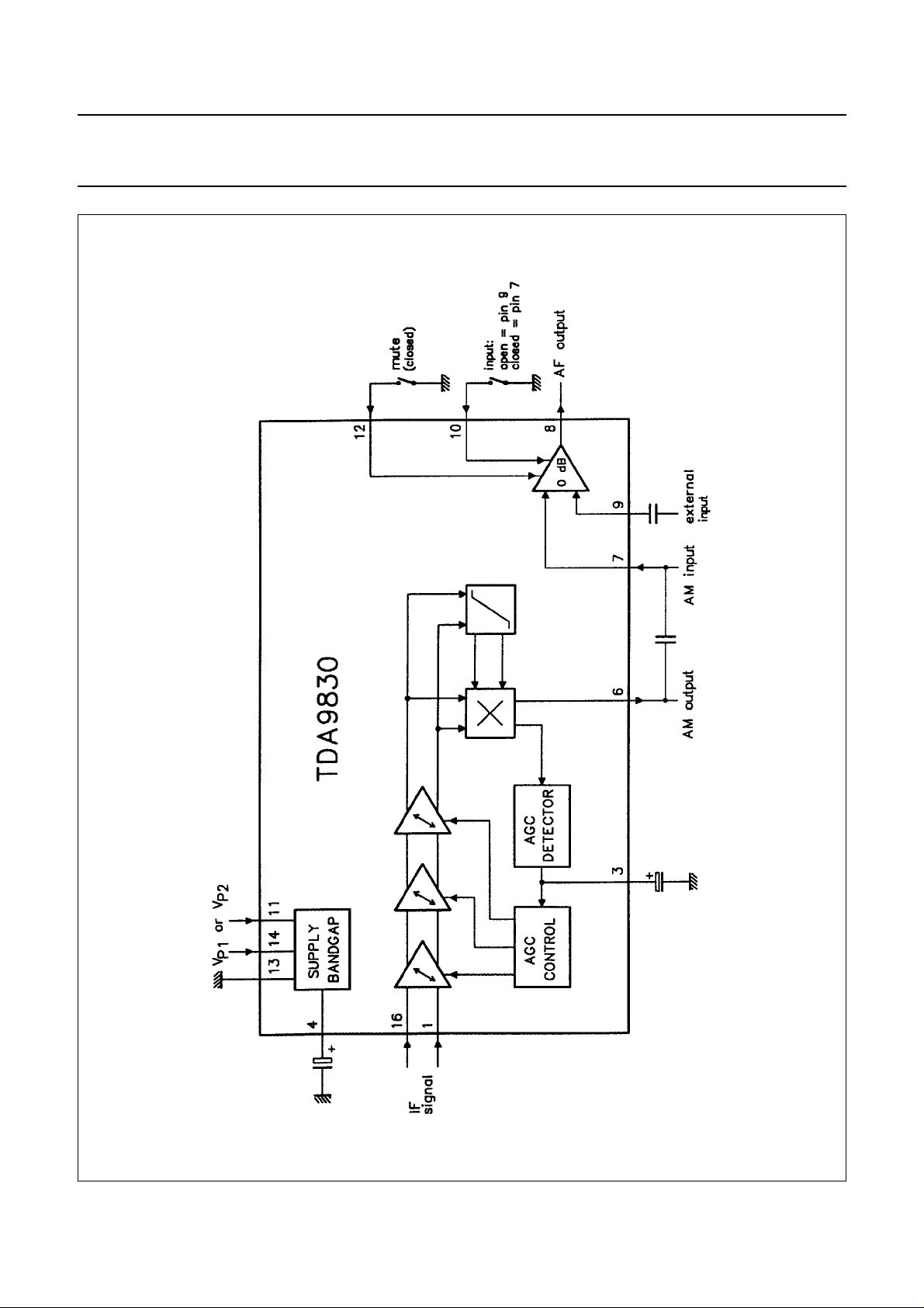
Fig.1 Block diagram.
Philips Semiconductors Product specification
TV sound AM-demodulator and audio source switch TDA9830
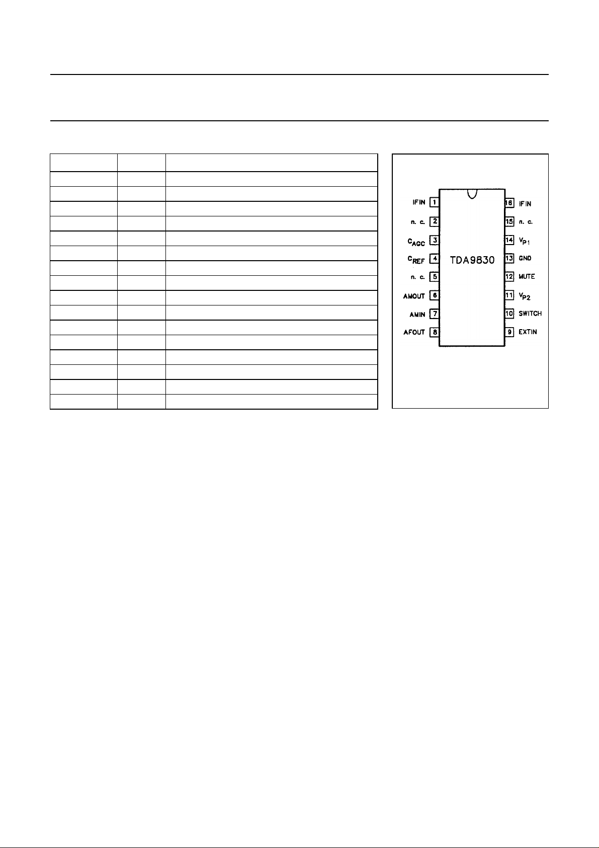
PINNING
SYMBOL PIN DESCRIPTION
IFIN 1 sound IF differential input signal
n.c. 2 not connected
C
AGC
C
REF
n.c. 5 not connected
AMOUT 6 AM demodulator output
AMIN 7 input signal (from AM) to audio switch
AFOUT 8 output signal from audio switch
EXTIN 9 input signal (from external) to audio switch
SWITCH 10 switch input select control
V
p2
MUTE 12 mute control
GND 13 ground (0 V)
V
p1
n.c. 15 not connected
IFIN 16 sound IF differential input signal
3 AGC capacitor
4 REF voltage filtering capacitor
11 supply voltage +12 V (alternative)
14 supply voltage +5 to +8 V
Fig.2 Pin configuration.
FUNCTIONAL DESCRIPTION
Sound IF input
The sound IF amplifier consists of
three AC-coupled differential
amplifier stages each with
approximately 20 dB gain. At the
output of each stage is a multiplier for
gain controlling (→ current
distribution gain control). The overall
control range is approximately −6 to
+60 dB and the frequency response
(−3 dB) of the IF amplifier is
approximately 6 to 70 MHz. The
steepness of gain control is
approximately 10 mV/dB.
IF AGC
The automatic gain control voltage to
maintain the AM demodulator output
signal at a constant level is generated
by a mean level detector. This
AGC-detector charges and
discharges the capacitor at pin 3
controlled by the output signal of the
AM-demodulator compared to an
internal reference voltage. The
maximum charge/discharge current is
approximately 5 µA. This value in
combination with the value of the
AGC capacitor and the AGC
steepness determines the lower
cut-off audio frequency and the
THD-figure at low modulation
frequency of the whole
AM-demodulator. Therefore a large
time constant has to be chosen which
leads to slow AGC reaction at IF level
change. To speed up the AGC in case
of IF signal jump from low to high
level, there is an additional
comparator built in, which can provide
additional discharge current from the
AGC capacitor up to 5 mA in a case of
overloading the AM demodulator by
the internal IF signal.
AM-demodulator
The IF amplifier output signal is fed to
a limiting amplifier (two stages) and to
a multiplier circuit. However the limiter
output signal (which is not any more
AM modulated) is also fed to the
multiplier, which provides AM
demodulation (in phase
demodulation). After lowpass filtering
≈ 400 kHz) for carrier rejection and
(f
g
buffering, the demodulator output
signal is present at pin 6. The AM
demodulator operates over a wide
frequency range, so that in
combination with the frequency
response of the IF amplifier
applications in a frequency range
from approximately 6 MHz up to
70 MHz are possible.
Audio switch
This circuit is an operational amplifier
with three input stages and internal
feedback network determining gain
(0 dB) and frequency response
(f
≈ 700 kHz). Two of the input
g
stages are connected to pin 7 and pin
9, the third input stage to an internal
reference voltage. Controlled by the
switching pins 10 and 12, one of the
three input stages can be activated
and a choice made between two
different AF signals or mute state.
The selected signal is present at
June 1994 4
Philips Semiconductors Product specification
TV sound AM-demodulator and audio source switch TDA9830
pin 8. The decoupling capacitors at
the input pins are needed, because
the internally generated bias voltage
for the input stages must not be
influenced by the application in order
to avoid DC-plop in case of switching.
The AM demodulator output is
designed to provide almost the same
DC voltage as the input bias voltage
of the audio switch. But there may be
spread between both voltages.
Therefore it is possible to connect pin
6 directly to pin 7 (without a
decoupling capacitor), but in this
event the DC-plop for switching can
increase up to 100 mV.
Reference circuit
This circuit is a band gap stabilizer in
combination with a voltage regulation
amplifier, which provides an internal
reference voltage of about 3.6 V
nearly independent from supply
voltage and temperature. This
reference voltage is filtered by the
capacitor at pin 4 in order to reduce
noise. It is used as a reference to
generate all important voltages and
currents of the circuit.
For application in 12 V power supply
concepts, there is an internal voltage
divider in combination with a
Darlington transistor in order to
reduce the supply voltage for all IC
function blocks to approximately 6 V.
This is necessary because of use of
modern high frequency IC
technology, where most of the used
integrated components are only
allowed to operate at maximum 9 V
supply voltage.
LIMITING VALUES
In accordance with the Absolute Maximum Rating System (IEC134).
SYMBOL PARAMETER MIN. MAX. UNIT
V
14−13
V
11−13
V
10, 12−13
T
amb
T
stg
supply voltage V
supply voltage V
P1
P2
−0.5 +8.9 V
−0.5 +13.3 V
switching voltage −0.5 VP+ 0.5 V
operating ambient temperature 0 +70 °C
storage temperature −25 +150 °C
Note to the limiting values
1. To avoid an inadmissible increase of ambient temperature, it is not allowed to short-circuit pin 11 for more than 10
seconds to ground.
THERMAL RESISTANCE
SYMBOL PARAMETER THERMAL RESISTANCE
R
th j-a
from junction to ambient in free air
SOT38 74 K/W
SOT109 100 K/W
June 1994 5
 Loading...