

Philips TDA9829T Datasheet

INTEGRATED CIRCUITS
DATA SH EET
TDA9829T
Downconverter for DVB
Product specification
File under Integrated Circuits, IC02
1998 Nov 09
Philips Semiconductors Product specification
Downconverter for DVB TDA9829T
FEATURES
• 5 V supply voltage
• Gain controlled IF-amplifier
GENERAL DESCRIPTION
The TDA9829T is an integrated circuit for DVB-IF
processing.
• Mixer for DVB-IF downconversion
• VCO for Quadrature Amplitude Modulation (QAM)
carrier recovery
• External VCO control
• Internal and external AGC
• DVB output level adjust via AGC adjust
• High level DVB operational output amplifier
• Mute switch for DVB output
• Tuner AGC with adjustable takeover point (TOP)
• AFC detector without extra reference circuit
• Stabilizer circuit for ripple rejection and to achieve
constant output signals.
QUICK REFERENCE DATA
SYMBOL PARAMETER CONDITIONS MIN. TYP. MAX. UNIT
V
P
I
P
V
3-4(rms)
∆ϕ
SSB
α
mute
I
12(sink)
supply voltage note 1 4.5 5.0 5.5 V
supply current 81 96 111 mA
input sensitivity (RMS value) −1 dB DVB signal at output − 100 150 µV
VCO phase noise f = 100 kHz; free-running 103 107 − dBc/Hz
mute attenuation note 2 − 36 − dB
sink current maximum tuner gain
1.5 2 2.6 mA
reduction; see Fig.3
CR
stps(US)
V
11(p-p)
B
−1dB
α
H
PSRR power supply ripple rejection at
control steepness ∆I14/∆fIF for
USA
output voltage
(peak-to-peak value)
fIF= 43.75 MHz;
notes 3 and 4; see Fig.4
CL< 15 pF; RL>5kΩ; with
internal AGC
0.7 0.98 1.3 µA/kHz
1.8 2.1 2.4 V
−1 dB bandwidth CL< 15 pF; RL>5kΩ 11 12 − MHz
suppression of in-band harmonics Vo= 2.0 V (p-p) 30 35 − dB
see Fig.5 26 36 − dB
pin 11
Notes
1. Performance may be decreased at V
= 4.5 V.
P
2. This parameter is not tested during production and is only given as application information for designing the television
receiver.
3. To match the AFC output signal to different tuning systems a current source output is provided. The test circuit is
given in Fig.4. The AFC-steepness can be changed by the resistors at pin 14.
4. Depending on the ratio ∆C/C0 of the LC resonant circuit of VCO (Q0> 50; C0=C
int+Cext
; see Table 2).
1998 Nov 09 2
Philips Semiconductors Product specification
Downconverter for DVB TDA9829T
ORDERING INFORMATION
TYPE
NUMBER
NAME DESCRIPTION VERSION
PACKAGE
TDA9829T SO20 plastic small outline package; 20 leads; body width 7.5 mm SOT163-1
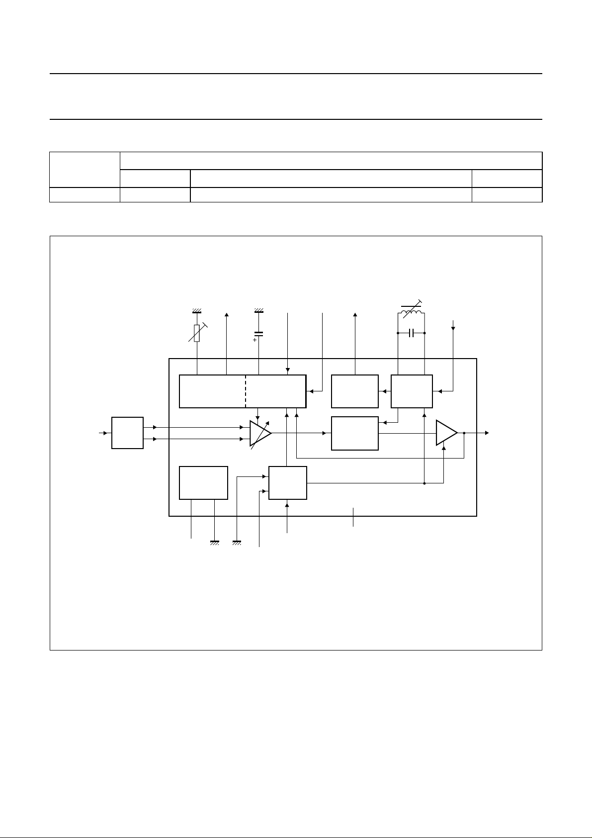
BLOCK DIAGRAM
15
DVB
external
VCO
control
V
10
VCO
11
V
oDVB
2 V (p-p)
handbook, full pagewidth
DVB-IF
input
DVB
IF filter
DVB
C
C
18125
AGC
adjust
AGC
AGC VCO1AFC VCO2TAGC
DVB
AGC
tuner
AGC
TOP
TADJ
TUNER
AGC
V
iIF1
3
4
V
iIF2
DVB
AGC
external
V
AGCAGCADJ
9
8
14
AFC
DETECTOR
DVB
MIXER
2 × f
PC
16
VCO
TWD
INTERNAL
VOLTAGE
STABILIZER
19 17 1 20 6
VPGND
+5 V
V
SID
MUTESWI
Fig.1 Block diagram.
LOGIC
AGCSWI
2, 7, 13
n.c.
TDA9829T
MHB219
1998 Nov 09 3
Philips Semiconductors Product specification
Downconverter for DVB TDA9829T
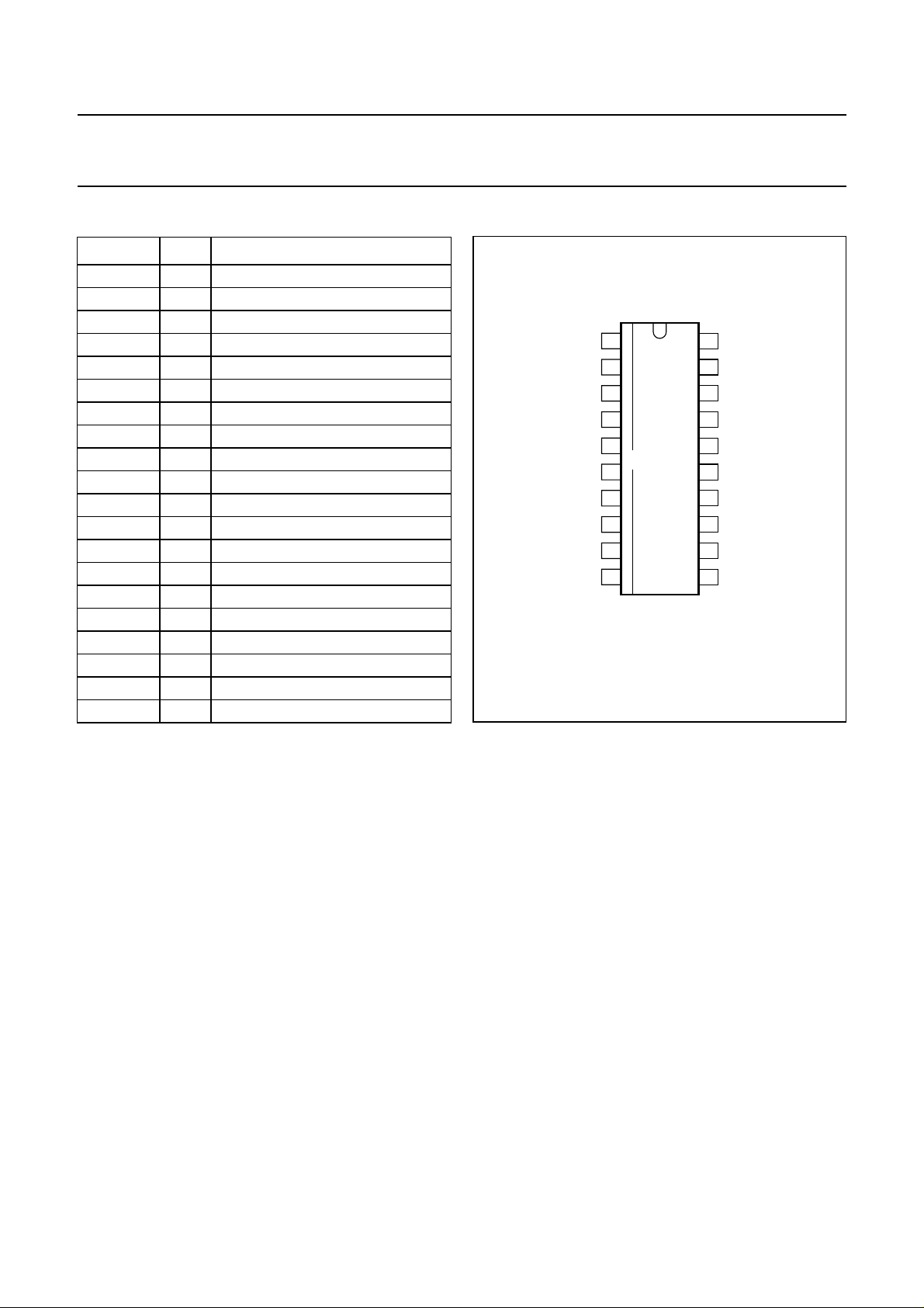
PINNING
SYMBOL PIN DESCRIPTION
V
SID
n.c. 2 not connected
V
iIF1
V
iIF2
TADJ 5 tuner AGC takeover adjust (TOP)
AGCSWI 6 AGC switch input
n.c. 7 not connected
V
AGC
AGCADJ 9 AGC adjust input
V
VCO
V
oDVB
TAGC 12 tuner AGC output
n.c. 13 not connected
AFC 14 AFC output
VCO1 15 VCO1 reference circuit
VCO2 16 VCO2 reference circuit
GND 17 ground
C
AGC
V
P
MUTESWI 20 mute switch input
1 SIF down input
3 IF differential input signal voltage 1
4 IF differential input signal voltage 2
8 AGC voltage input
10 VCO control voltage
11 DVB output
18 AGC capacitor
19 supply voltage (+5 V)
handbook, halfpage
V
1
SID
2
n.c.
V
3
iIF1
V
4
iIF2
TADJ
5
TDA9829T
V
V
n.c.
AGC
VCO
6
7
8
9
10
AGCSWI
AGCADJ
Fig.2 Pin configuration.
MHB220
20
19
18
17
16
15
14
13
12
11
MUTESWI
V
P
C
AGC
GND
VCO2
VCO1
AFC
n.c.
TAGC
V
oDVB
1998 Nov 09 4
Philips Semiconductors Product specification
Downconverter for DVB TDA9829T
FUNCTIONAL DESCRIPTION
Vision IF amplifier
The vision IF amplifier consists of three AC-coupled
differential amplifier stages. Each differential stage
comprises a feedback network controlled by emitter
degeneration to control the IF gain.
VCO, Travelling Wave Divider (TWD) and AFC
The VCO operates with a resonance circuit (with L and C
in parallel) at double the IF frequency plus symbol
frequency. The VCO is controlled by integrated variable
capacitors. The control voltage required to tune the VCO
from its free-running frequency to its actual frequency is
fed to the capacitors. This control voltage is amplified and
converted into a current which represents the AFC output
signal. At centre frequency the AFC output current is equal
to zero.
The oscillator signal is divided-by-two with a TWD which
generates a differential output signal for downconverting
the IF signal.
DVB mixer
The gain controlled DVB-IF signal is downconverted to the
symbol frequency by use of a four quadrant multiplier.
The conversion signal is provided by the VCO and TWD.
DVB AGC and tuner AGC
The AGC detector charges/discharges the AGC capacitor
to the required voltage for setting the IF and tuner gain in
order to keep the DVB signal at a constant level.
A peak detector is used for the DVB AGC. The peak value
of (digital) the QAM signal is detected and controlled to a
constant value by the variable gain IF amplifier.
The detector bandwidth is adapted to the symbol
frequency (3 to 11 MHz). The external AGC time constant
is given by the IF AGC capacitor at pin 18.
The AGC capacitor voltage is transferred to an internal IF
control signal, and is fed to the tuner AGC to generate the
tuner AGC output current (open-collector output).
The tuner AGC takeover point can be adjusted. This
allows the tuner and the SWIF filter to be matched to
achieve the optimum IF input level.
The DVB output signal (V
of ±3 dB by a control voltage (∆V
) can be adjusted in a range
oDVB
) at pin 9. The internal
adj
AGC can be switched off at pin 6 and the IF gain can be
controlled by an external voltage at pin 8. The tuner AGC
is active in both instances.
DVB output amplifier
The output amplifier for the DVB signal has a high
bandwidth and delivers a 2 V (p-p) signal. The amplifier
can be switched to a mute state forced by the signal at
pin 20.
Internal voltage stabilizer
A band gap circuit internally generates a voltage of
approximately 1.25 V, independent of supply voltage and
temperature. A voltage regulator circuit, connected to this
voltage, produces a constant voltage of 3.6 V which is
used as an internal reference voltage.
LIMITING VALUES
In accordance with the Absolute Maximum Rating System (IEC 134).
SYMBOL PARAMETER CONDITIONS MIN. MAX. UNIT
V
P
V
n
supply voltage (pin 19) maximum chip temperature of 125 °C 0 5.5 V
voltage at pins
0V
P
1 to 10, 13, 14 and 18 to 20
t
sc(max)
V
12
T
stg
T
amb
V
es
maximum short-circuit time − 10 s
tuner AGC output voltage 0 13.2 V
storage temperature −25 +150 °C
operating ambient temperature −20 +70 °C
electrostatic handling voltage machine model class B −300 +300 V
1998 Nov 09 5
V
Philips Semiconductors Product specification
Downconverter for DVB TDA9829T
THERMAL CHARACTERISTICS
SYMBOL PARAMETER CONDITIONS VALUE UNIT
R
th(j-a)
thermal resistance from junction
to ambient
CHARACTERISTICS
=5V; T
V
P
=25°C; see Table 1 for input frequencies; input level V
amb
taken in Fig.8; unless otherwise specified.
SYMBOL PARAMETER CONDITIONS MIN. TYP. MAX. UNIT
Supply (pin 19)
V
P
I
P
IF amplifier (measured at f
∆V
(3-4)(rms)
V
i(3-4)(rms)
supply voltage note 1 4.5 5.0 5.5 V
supply current 81 96 111 mA
= 43.75 MHz; pins 3 and 4)
IF
input sensitivity (RMS value) −1 dB DVB signal at output − 100 150 µV
maximum input signal level
(RMS value)
∆G
IF
total gain control IF amplifier 59 64 − dB
tilt for ∆f ±3 MHz f
R
i(3-4)(diff)
C
i(3-4)(diff)
input resistance (differential) note 2 − 2.2 − kΩ
input capacitance (differential) note 2 − 1.7 − pF
DVB mixer and VCO (pins 10, 15 and 16); see notes 4 and 5 and Table 1
f
VCO(max)
f
VCO(US)
f
VCO(EU)
V
ref(rms)
maximum oscillator frequency 2(fIF+fs) 125 130 − MHz
VCO frequency for USA 2(fIF+fs) − 97.5 − MHz
VCO frequency for Europe 2(fIF+fs) − 86.0 − MHz
oscillator voltage swing between
pins 15 and 16 (RMS value)
∆ϕ
V
R
VCO
SSB
i(VCO)
VCO phase noise f = 100 kHz; free-running 103 107 − dBc/Hz
VCO control range (pin 10) see Figs 6 and 7 0 − V
VCO control input resistance
(pin 10)
CR
stps(VCO)
control steepness ∆fs/∆V
10
in free air 85 K/W
= 10 mV (RMS value); measurements
iIF(3−4)
1 dB DVB signal at output 140 200 − mV
= 6.9 MHz; 40 dB gain − 0.5 1 dB
s
− 60 − mV
P
V
50 63 76 kΩ
see Figs 6 and 7
DVB (USA) − 0.29 − MHz/V
DVB (Europe) − 0.40 − MHz/V
DVB output amplifier (pins 11 and 20)
V
o(DVB)(p-p)
DVB output signal (QAM)
(peak-to-peak value)
I
bias(int)
DC internal bias current for
emitter-follower (pin 11)
I
sink(max)
maximum AC and DC output
sink current (pin 11)
I
source(max)
maximum AC and DC output
source current (pin 11)
1998 Nov 09 6
1.8 2.1 2.4 V
1.9 2.3 2.7 mA
1.5 −−mA
2.0 −−mA
 Loading...