

Philips tda9820 DATASHEETS

INTEGRATED CIRCUITS
DATA SH EET
TDA9820
Multistandard/dual channel TV FM
intercarrier sound demodulator
Product specification
Supersedes data of March 1991
File under Integrated Circuits, IC02
1996 Nov 20
Philips Semiconductors Product specification
Multistandard/dual channel TV FM
TDA9820
intercarrier sound demodulator
FEATURES
• Multistandard application for sound standards M, B/G, I
and D/K
• Two alignment-free PLL FM demodulators
• Four-input source selector for one of the two FM
demodulators
• Automatic second sound carrier mute
• Mono and dual channel application
• Low power consumption
• Few external components required.
QUICK REFERENCE DATA
SYMBOL PARAMETER CONDITIONS MIN. TYP. MAX. UNIT
V
P
I
P
I
M
V
i(rms)
V
o(rms)
SN+
-------------N
α
8/7
supply voltage (pin 14) 4.5 5.0 8.8 V
supply current (pin 14) 23 30 37 mA
AC peak current (pins 7 and 8) −−1.5 mA
input signal (RMS value) − 150 250 µV
output signal (pins 7 and 8; RMS value) ∆fi= ±50 kHz 0.4 0.5 0.6 V
signal plus noise-to-noise ratio
(pins 7 and 8)
crosstalk attenuation f = 50 to 12500 Hz 60 70 − dB
RR supply voltage ripple rejection
(pins 7 and 8)
T
amb
operating ambient temperature 0 − 70 °C
GENERAL DESCRIPTION
The TDA9820 is a monolithic, integrated, multistandard TV
FM intercarrier sound demodulator for all FM standards.
The circuit contains two separate FM demodulators using
Phase Locked Loop (PLL) reference frequency
generation. The circuit requires a minimum number of
external components.
SN+
--------------
in accordance with
N
40 dB=
64 68 − dB
“CCIR 468-3”
< 200 mV; f = 70 Hz 16 20 − dB
V
RR
ORDERING INFORMATION
PACKAGE
TYPE NUMBER
NAME DESCRIPTION VERSION
TDA9820 DIP16 plastic dual in-line package; 16 leads (300 mil); long body SOT38-1
TDA9820T SO16 plastic small outline package; 16 leads; body width 7.5 mm SOT162-1
1996 Nov 20 2
Philips Semiconductors Product specification
Multistandard/dual channel TV FM
intercarrier sound demodulator
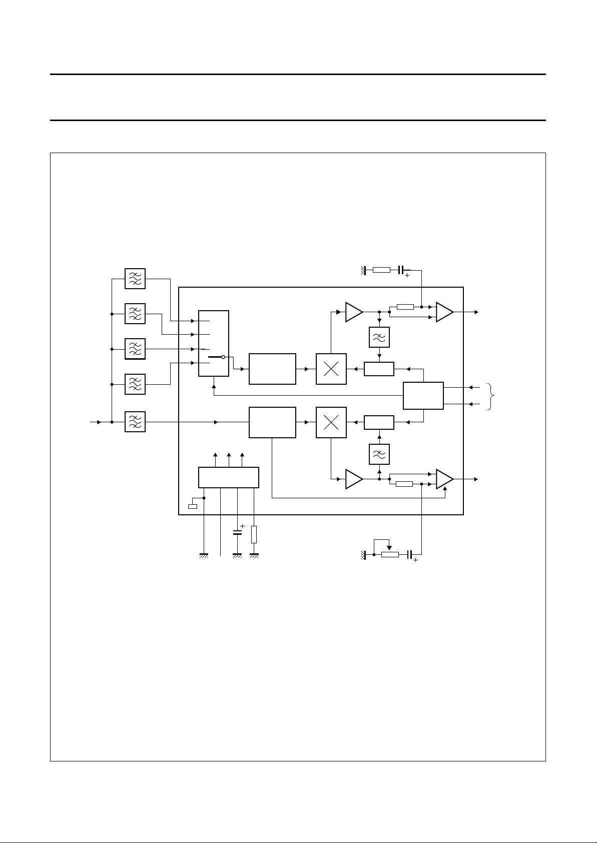
BLOCK DIAGRAM
handbook, full pagewidth
intercarrier
4.5 MHz (M)
5.5 MHz (B/G)
6.0 MHz (I)
6.5 MHz (D/K)
4.72 MHz (M)
or
5.74 MHz (B/G)
or
6.74 MHz (D/K)
3
1
16
2
15
SUPPLY
V =
P
4.5 to 8.8 V
TDA9820
7-STAGE
LIMITER
AMPLIFIER 1
7-STAGE
LIMITER
AMPLIFIER 2
11121413
VCO
ref
mute
R
s
VCO 1
VCO 2
optional stereo
channel separation
adjustment
(1)
R
(1)
pot
9
CONTROL
UNIT
10
+
−
−
+
MHA420
TDA9820
8
V
AF1
S
5
1
S
6
2
7
V
AF2
standard
switch
(1) Resistor and potentiometer between capacitor and earth are inserted if adjustment of stereo channel separation is required.
1996 Nov 20 3
Fig.1 Block diagram.
Philips Semiconductors Product specification
Multistandard/dual channel TV FM
intercarrier sound demodulator
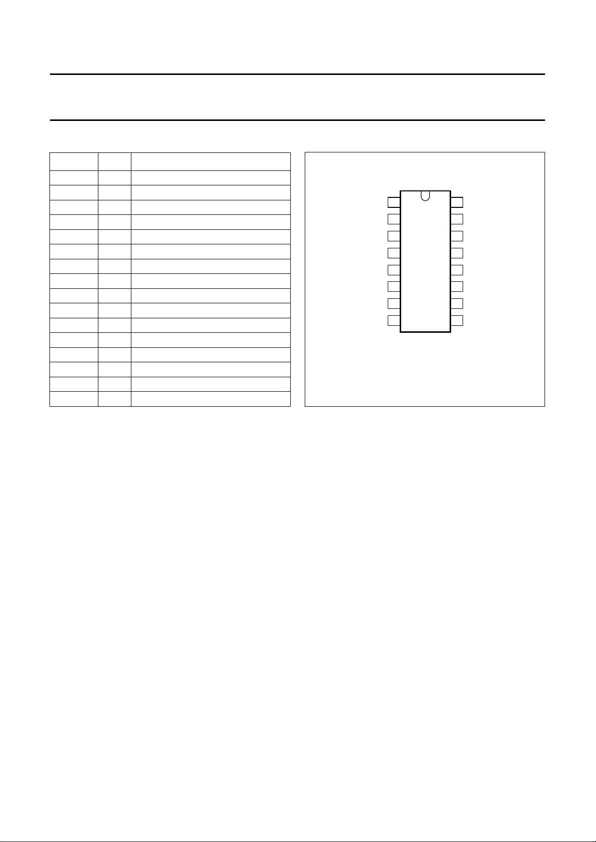
PINNING
SYMBOL PIN DESCRIPTION
IN
1(B/G)
IN
1(D/K)
IN
1(M)
n.c. 4 not connected
S
1
S
2
V
AF2
V
AF1
C
1
C
2
VCO
ref
C
STAB
GND 13 ground
V
P
IN
2
IN
1(I)
1 intercarrier input 1 at 5.5 MHz
2 intercarrier input 1 at 6.5 MHz
3 intercarrier input 1 at 4.5 MHz
5 standard switch bit 1 input
6 standard switch bit 2 input
7 audio output voltage 2
8 audio output voltage 1
9 decoupling capacitor 1
10 decoupling capacitor 2
11 VCO reference
12 supply voltage stabilization
14 supply voltage
15 intercarrier input 2
16 intercarrier input 1 at 6.0 MHz
handbook, halfpage
IN
IN
1(B/G)
1(D/K)
IN
1(M)
n.c.
V
AF2
V
AF1
1
2
3
4
1
2
5
6
7
8
TDA9820
MHA529
S
S
Fig.2 Pin configuration.
TDA9820
IN
16
1(I)
IN
15
2
V
14
P
13
GND
C
12
STAB
VCO
11
ref
C
10
2
C
9
1
1996 Nov 20 4
Philips Semiconductors Product specification
Multistandard/dual channel TV FM
intercarrier sound demodulator
FUNCTIONAL DESCRIPTION
The complete circuit consists of two separate channels,
each consisting of a limiter-amplifier, FM demodulator and
AF amplifier. Circuit operation is also described in Fig.1.
Source selector
The intercarrier signal is fed through external ceramic
band-pass filters which are tuned to the sound carrier
frequencies.
One of the four filtered sound carriers from
pins 1, 2, 3 or 16 is fed to limiter-amplifier 1 via the
appropriate electronic switch in the source selector.
The electronic switch of the sound carrier is selected by
the control unit (see Table 1).
The second sound carrier of the intercarrier signal is
directly fed from pin 15 to limiter-amplifier 2.
FM demodulators
TDA9820
Stereo channel separation adjustment (optional)
Optimal stereo channel separation is achieved by
adjusting V
1. V
AF1
capacitor at pin 9
2. V
AF2
DC decoupling capacitor on pin 10 to the same
voltage as V
Second sound carrier mute
The output of the second FM demodulator is muted when
the signal level (signal and/or noise) at pin 15 is less than
typically 0.5 mV (RMS value). This avoids an incorrect
stereo or dual sound identification when a mono signal is
transmitted. Therefore, with a mono transmission, there is
no audio output at pin 7. When the signal level at pin 15 is
greater than typically 1.0 mV (RMS value) mute is
switched off.
(pin 8) and V
AF1
by a resistor in series with the DC decoupling
by a variable resistor in series with the
.
AF1
(pin 7) as follows:
AF2
Each limiter-amplifier is AC-coupled into a
FM demodulator. The integrated FM demodulator PLLs
are alignment-free. The FM demodulator outputs are
amplified to 500 mV (RMS value). High amplification and
DC error signals of the PLLs, which are superimposed on
the FM demodulator outputs, require DC decoupling at
pins 9 and 10 of the AF amplifier inputs.
Table 1 Logic table; note 1
STANDARD
B/G 1 1 5.5 5.74 pin 1
M 1 0 4.5 4.72 pin 3
I 0 1 6.0 off pin 16
D/K 0 0 6.5 6.74 pin 2
Note
1. In columns S1 and S2: 0 = LOW and 1 = HIGH.
S1
(PIN 5)S2(PIN 6)
FREQUENCY VCO1
(MHz)
Control unit
The control unit selects the required sound standard
according to the voltages on pin 5 and pin 6. The control
unit performs the following:
1. selects the free-running frequencies of VCO1 and
VCO2
2. switches the source selector (the four possible
combinations are shown in Table 1).
FREQUENCY VCO2
(MHz)
SOURCE SELECTOR
CONNECTION
1996 Nov 20 5
 Loading...