


INTEGRATED CIRCUITS
DATA SH EET
TDA9817; TDA9818
Single/multistandard VIF/SIF-PLL
and FM-PLL/AM demodulators
Preliminary specification
Supersedes data of 1997 May 12
File under Integrated Circuits, IC02
2001 Oct 19

Philips Semiconductors Preliminary specification
Single/multistandard VIF/SIF-PLL and
FM-PLL/AM demodulators
FEATURES
• 5 V supply voltage
• Applicable for Intermediate Frequencies (IFs) of
38.9, 45.75 and 58.75 MHz
• Gain controlled wide band Video IF (VIF) amplifier
(AC-coupled)
• True synchronous demodulation with active carrier
regeneration (very linear demodulation, good
intermodulation figures, reduced harmonics and
excellent pulse response)
• Robustness for over-modulation better than 105% due
to gated phase detector at L/L accent standard and
PLL-bandwidth controlat negative modulated standards
• Voltage Controlled Oscillator (VCO) frequency
switchablebetweenL and L accent(alignmentexternal)
picture carrier frequency
• VIF Automatic Gain Control (AGC) detector for gain
control, operating as peak sync detector for B/G, peak
white detector for L; signal controlled reaction time for L
• Tuner AGC with adjustable TakeOver Point (TOP)
• Automatic Frequency Control (AFC) detector without
extra reference circuit
TDA9817; TDA9818
• AC-coupled limiter amplifier for sound intercarrier signal
• Alignment-free FM Phase-Locked Loop (PLL)
demodulator with high linearity
• Sound IF (SIF) input for single reference Quasi Split
Sound (QSS) mode (PLL controlled); SIF AGC detector
for gain controlled SIF amplifier; single reference QSS
mixer able to operate in high performance single
reference QSS mode and in intercarrier mode
• AM demodulator without extra reference circuit
• Stabilizer circuit for ripple rejection and to achieve
constant output signals
• ElectroStatic Discharge (ESD) protection for all pins.
GENERAL DESCRIPTION
The TDA9817 is an integrated circuit for single standard
vision IF signal processing and FM demodulation.
The TDA9818 is an integrated circuit for multistandard
vision IF signal processing, sound AM and FM
demodulation.
ORDERING INFORMATION
TYPE NUMBER
NAME DESCRIPTION VERSION
TDA9817 SDIP24 plastic shrink dual in-line package; 24 leads (400 mil) SOT234-1
TDA9817T SO24 plastic small outline package; 24 leads; body width 7.5 mm SOT137-1
TDA9817TS SSOP24 plastic shrink small outline package; 24 leads; body width 5.3 mm SOT340-1
TDA9818 SDIP24 plastic shrink dual in-line package; 24 leads (400 mil) SOT234-1
TDA9818T SO24 plastic small outline package; 24 leads; body width 7.5 mm SOT137-1
TDA9818TS SSOP24 plastic shrink small outline package; 24 leads; body width 5.3 mm SOT340-1
PACKAGE
2001 Oct 19 2

Philips Semiconductors Preliminary specification
Single/multistandard VIF/SIF-PLL and
TDA9817; TDA9818
FM-PLL/AM demodulators
QUICK REFERENCE DATA
SYMBOL PARAMETER CONDITIONS MIN. TYP. MAX. UNIT
V
P
I
P
V
i(VIF)(rms)
V
o(CVBS)(p-p)
B
v(−3dB)
S/N
W
α
IM(1.1)
α
IM(3.3)
α
H(sup)
V
i(SIF)(rms)
V
o(FM)(rms)
V
o(AM)(rms)
THD
audio
S/N
W(audio)
supply voltage 4.5 5 5.5 V
supply current 76 90 104 mA
vision IF input signal voltagesensitivity
−1 dB video at output − 60 100 µV
(RMS value)
video output signal voltage
0.97 1.1 1.23 V
(peak-to-peak value)
−3 dB video bandwidth on pin CVBS B/G and L standard;
78−MHz
CL< 50 pF; RL>1kΩ; AC load
weighted signal-to-noise ratio for video 56 60 − dB
intermodulation attenuation at ‘blue’ f = 1.1 MHz 58 64 − dB
intermodulation attenuation at ‘blue’ f = 3.3 MHz 58 64 − dB
suppression of video signal harmonics 35 40 − dB
sound IF input signal voltage
−3 dB at intercarrier output − 50 100 µV
sensitivity (RMS value)
audio output signal voltage for FM
(RMS value)
B/G standard; 27 kHz,
54% modulation
M/N standard;
0.4 0.5 0.6 V
0.36 0.45 0.54 V
25 kHz modulation
audio output signal voltage for AM
L standard; 54% modulation 0.4 0.5 0.6 V
(RMS value)
total harmonic distortion audio signal 54% modulation
FM − 0.2 0.5 %
AM − 0.5 1.0 %
weighted signal-to-noise ratio audio
54% modulation
signal
FM 55 60 − dB
AM 47 53 − dB
2001 Oct 19 3
This text is here in white to force landscape pages to be rotated correctly when browsing through the pdf in the Acrobat reader.This text is here in
_white to force landscape pages to be rotated correctly when browsing through the pdf in the Acrobat reader.This text is here inThis text is here in
white to force landscape pages to be rotated correctly when browsing through the pdf in the Acrobat reader. white to force landscape pages to be ...
2001 Oct 19 4
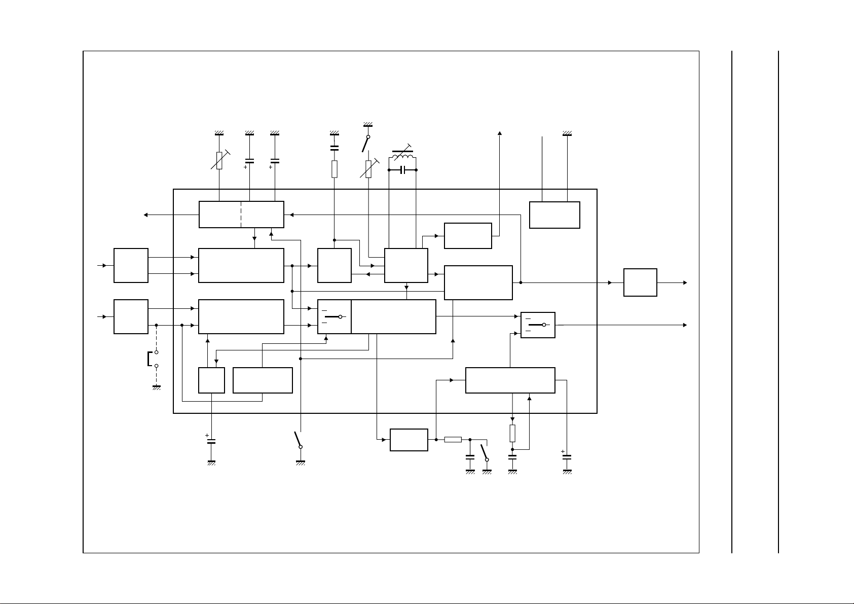
L/L accent switch
and adjust
2 × f
pc
C
VIF
SAW
SIF
SAW
TAGC
VIF1
VIF2
SIF1
SIF2
C
14
TUNER
AGC
1
2
23
24
VIF AMPLIFIER FPLL
SIF AMPLIFIER
VAGC
BLTOP LADJ VCO2 VCO1
(1)
422
VIF
AGC
T
PLL
615
(1)
7
QSS MIXER
INTERCARRIER MIXER
AM DEMODULATOR
VCO
TWD
AFC
DETECTOR
VIDEO
DEMODULATOR
AND AMPLIFIER
AFC
V
P
VOLTAGE
REFERENCE
GND
2021171819
16
8
CVBS
1.1 V (p-p)
AF
SOUND
TRAP
video
1 V (p-p)
audio
BLOCK DIAGRAM
Philips Semiconductors Preliminary specification
Single/multistandard VIF/SIF-PLL and
FM-PLL/AM demodulators
intercarrier
mode
SIF
AGC
(1) Not connected for TDA9817, TDA9817T and TDA9817TS.
INTERCARRIER
MODE SWITCH
5
C
SAGC
standards
selection
switch
(1)
3
TDA9817
TDA9818
Fig.1 Block diagram.
12
QSSSTD
5.5 MHz
handbook, full pagewidth
13
FM
FM-PLL
DEMODULATOR
10 11
9
V
in
de-em
mute
switch
C
de-em
C
DEC
MHA663
TDA9817; TDA9818
Philips Semiconductors Preliminary specification
Single/multistandard VIF/SIF-PLL and
FM-PLL/AM demodulators
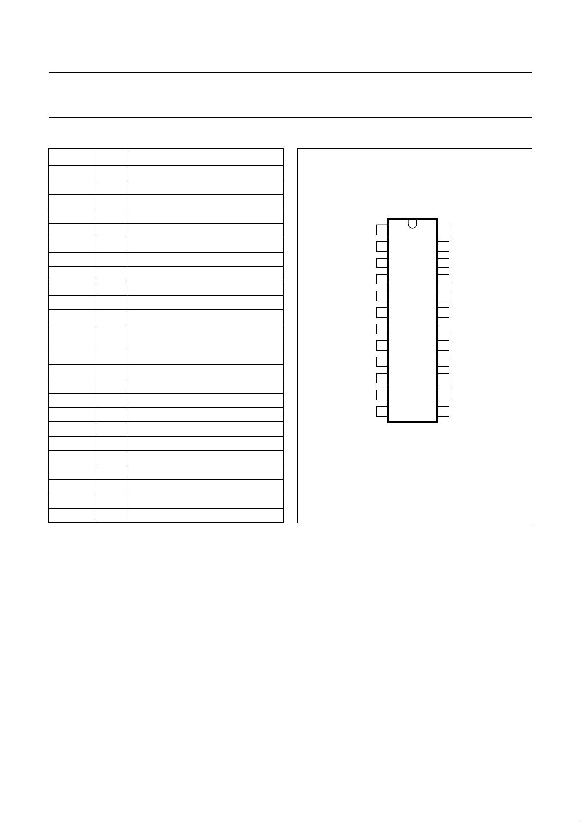
PINNING
SYMBOL PIN DESCRIPTION
VIF1 1 VIF differential input signal voltage 1
VIF2 2 VIF differential input signal voltage 2
STD 3 standards selection switch; note 1
C
VAGC
C
SAGC
T
PLL
LADJ 7 L/L accent switch and adjust; note 1
AF 8 audio output
V
de-em
C
de-em
C
DEC
QSS 12 single reference QSS/intercarrier
FM
in
TAGC 14 tuner AGC output
C
BL
CVBS 16 composite video output voltage
AFC 17 AFC output
VCO1 18 VCO1 resonance circuit
VCO2 19 VCO2 resonance circuit
GND 20 ground
V
P
TOP 22 tuner AGC takeover point adjust
SIF1 23 SIF differential input signal voltage1
SIF2 24 SIF differential input signal voltage2
4 VIF AGC capacitor
5 SIF AGC capacitor
6 PLL filter
9 de-emphasis output
10 de-emphasis input
11 decoupling capacitor
output voltage
13 sound intercarrier input voltage
15 black level detector; note 1
21 supply voltage
handbook, halfpage
C
C
LADJ
V
C
(1) Not connected for TDA9817.
VIF1
VIF2
STD
VAGC
SAGC
T
PLL
de-em
de-em
C
DEC
QSS
AF
1
2
(1)
3
4
5
6
(1)
7
8
9
10
11
12
Fig.2 Pin configuration SDIP24.
TDA9817; TDA9818
SIF2
24
SIF1
23
TOP
22
V
21
P
GND
20
VCO2
MHA664
19
VCO1
18
AFC
17
CVBS
16
(1)
C
15
BL
TAGC
14
13
FM
in
TDA9818
TDA9817
Note
1. Not connected for TDA9817, TDA9817T and
TDA9817TS.
2001 Oct 19 5
Philips Semiconductors Preliminary specification
Single/multistandard VIF/SIF-PLL and
FM-PLL/AM demodulators
handbook, halfpage
STD
C
VAGC
C
SAGC
T
LADJ
V
de-em
C
de-em
C
VIF1
VIF2
PLL
AF
DEC
QSS
1
2
(1)
3
4
5
6
TDA9818T
7
8
9
10
11
12
TDA9817T
(1)
MGU397
24
SIF2
23
SIF1
22
TOP
21
V
P
GND
20
VCO2
19
VCO1
18
AFC
17
CVBS
16
(1)
15
C
BL
14
TAGC
FM
13
in
handbook, halfpage
STD
C
VAGC
C
SAGC
T
LADJ
V
de-em
C
de-em
C
VIF1
VIF2
PLL
AF
DEC
QSS
(1)
(1)
10
11
12
TDA9817; TDA9818
1
2
3
4
5
6
TDA9818TS
TDA9817TS
7
8
9
MGU398
24
SIF2
23
SIF1
22
TOP
21
V
P
20
GND
19
VCO2
18
VCO1
17
AFC
CVBS
16
(1)
15
C
BL
14
TAGC
FM
13
in
(1) Not connected for TDA9817T.
Fig.3 Pin configuration SO24.
2001 Oct 19 6
(1) Not connected for TDA9817TS.
Fig.4 Pin configuration SSOP24.

Philips Semiconductors Preliminary specification
Single/multistandard VIF/SIF-PLL and
FM-PLL/AM demodulators
FUNCTIONAL DESCRIPTION
The integrated circuit comprises the functional blocks as
shown in Fig.1:
• Vision IF amplifier and VIF AGC detector
• Tuner AGC
• Frequency Phase Locked Loop detector (FPLL)
• VCO, Travelling Wave Divider (TWD) and AFC
• Video demodulator and amplifier
• Sound IF amplifier and SIF AGC
• Single reference QSS mixer
• AM demodulator
• FM-PLL demodulator
• Audio Frequency (AF) signal processing
• Internal voltage stabilizer.
Vision IF amplifier and VIF AGC detector
The vision IF amplifier consists of three AC-coupled
differential amplifier stages. Each differential stage
comprises a feedback network controlled by emitter
degeneration.
The AGC detector generates therequired VIF gain control
voltage for constant video output by charging/discharging
the AGC capacitor. Therefore for negative video
modulation the sync level and for positive video
modulation the peak white level of the video signal is
detected. In order to reduce the reaction time for positive
modulation, where a very large time constant is needed,
an additional level detector increases the discharging
current of the AGC capacitor (fast mode) in the event of a
decreasing VIF amplitude step. The additional level
information is given by the black-level detector voltage.
Tuner AGC
The AGC capacitor voltage is converted to an internal
IF control signal, and is fed to the tuner AGC to generate
the tuner AGC output current at pin TAGC (open-collector
output). The tuner AGC takeover point can be adjusted at
pin TADJ. This allows to match the tuner to the SAW filter
in order to achieve the optimum IF input level.
Frequency Phase Locked Loop detector (FPLL)
The VIF-amplifier output signal is fed into a frequency
detector and into a phase detector via a limiting amplifier.
During acquisition the frequency detector produces a
DC current proportional to the frequency difference
between the input and the VCO signal. After frequency
lock-in the phase detector produces a DC current
TDA9817; TDA9818
proportionalto the phase differencebetween the VCO and
the input signal. The DC current of either frequency
detector or phase detector is converted into a DC voltage
viathe loop filter, whichcontrols the VCO frequency.Inthe
event of positive modulated signals the phase detector is
gated by composite sync in order to avoid signal distortion
for overmodulated VIF signals.
VCO, Travelling Wave Divider (TWD) and AFC
The VCO operates with a resonance circuit (with L and C
in parallel) at double the picture carrier frequency. The
VCO is controlled by two integrated variable capacitors.
The control voltage required to tune the VCO from its
free-running frequency to actually double the picture
carrier frequency is generated by the frequency-phase
detector (FPLL) and fed via the loop filter to the first
variable capacitor. This control voltage is amplified and
additionally converted into a current which represents the
AFC output signal. At centre frequency the AFC output
current is equal to zero.
For TDA9818: the VCO centre frequency can be
decreased (required for L accent standard) by activating
an additional internal capacitor. This is achieved by using
the L accent switch. In this event the second variable
capacitor can be controlled by a variable resistor at the
L accentswitchforsettingtheVCOcentrefrequencytothe
required L accent value.
The oscillator signal is divided by 2 with a TWD which
generates two differential output signals with a 90 degree
phase difference independent of the frequency.
Video demodulator and amplifier
The video demodulator is realized by a multiplier which is
designed for low distortion and large bandwidth. The
vision IF input signal is multiplied with the ‘in phase’ signal
of the travelling wave divider output. In the demodulator
stage the video signal polarity can be switched in
accordance with the TV standard.
The demodulator output signal is fed via an integrated
low-pass filter for attenuation of the carrier harmonics to
the video amplifier. The video amplifier is realized by an
operational amplifier with internal feedback and high
bandwidth. A low-pass filter is integrated to achieve an
attenuation of the carrier harmonics for B/G and
L standard. The standard dependent level shift in this
stage delivers the same sync level for positive and
negative modulation. The video output signal at pin CVBS
is 1.1 V (p-p) for nominal vision IF modulation, in order to
achieve 1 V (p-p) at sound trap output.
2001 Oct 19 7

Philips Semiconductors Preliminary specification
Single/multistandard VIF/SIF-PLL and
FM-PLL/AM demodulators
Sound IF amplifier and SIF AGC
The sound IF amplifier consists of two AC-coupled
differential amplifier stages. Each differential stage
comprises a controlled feedback network provided by
emitter degeneration.
The SIF AGC detector is related to the SIF input signal
(average level of AM or FM carrier) and controls the SIF
amplifier to provide a constant SIF signal to the
AM demodulator and single reference QSS mixer. At
L standard (AM sound) the SIF AGC reaction time is set to
‘slow’ for nominal video conditions. But with a decreasing
VIF amplitude step the SIF AGC is set to ‘fast’ mode
controlled by the VIF AGC detector. In FM mode this
reaction time is always ‘fast’.
Single reference QSS mixer
The single reference QSS mixeris realized by a multiplier.
The SIF amplifier output signal is fed to the single
reference QSS mixer and converted to intercarrier
frequency by the regenerated picture carrier (VCO). The
mixer output signal is fed via a high-pass for attenuation of
the video signal components to the output pin QSS. With
this system a high performance hi-fi stereo sound
processing can be achieved.
For a simplified application without a sound IF SAW filter
the single reference QSS mixer can be switched to the
intercarrier mode byconnecting pin SIF2 to ground. In this
mode the sound IF passes the vision IF SAW filter and the
composite IF signal is fed to the single reference QSS
mixer. This IF signal is multiplied with the 90 degree TWD
output signal for converting the sound IF to intercarrier
frequency. This composite intercarrier signal is fed to the
output pin QSS, too. By using this quadrature detection,
the low frequency video signals are removed.
AM demodulator
The AM demodulator is realized by a multiplier. The
modulated SIF amplifier output signal is multiplied in
phase with the limited (AM is removed) SIF amplifier
output signal. The demodulator output signal is fed via an
integrated low-pass filter for attenuation of the carrier
harmonics to the AF amplifier.
TDA9817; TDA9818
FM-PLL demodulator
The FM-PLL demodulator consists of a limiter and an
FM-PLL. The limiter provides the amplification and
limitation of the FM sound intercarrier signal. The result is
high sensitivity and AM suppression. The amplifier
consists of 7 stages which are internally AC-coupled in
order to minimize the DC offset.
Furthermore the AF output signal can be muted by
connecting a resistor between the limiter input pin FM
and ground.
TheFM-PLL consists of anintegrated relaxation oscillator,
an integrated loop filter and a phase detector. The
oscillator is locked to the FM intercarrier signal, output
from the limiter. As a result of locking, the oscillator
frequency tracks with the modulation of the input signal
and the oscillator control voltage is superimposed by the
AF voltage. The FM-PLL operates as an FM demodulator.
Audio Frequency signal processing
The AF amplifier consists of two parts:
1. The AF pre-amplifier for FM sound is an operational
amplifier with internal feedback, high gain and high
common mode rejection. The AF voltage from the
PLL demodulator, by principle a small output signal, is
amplified by approximately 33 dB. The low-pass
characteristicoftheamplifierreducestheharmonicsof
the intercarrier signal at the sound output terminal
pin V
sound is applied. An additional DC control circuit is
implemented to keep the DC level constant,
independent of process spread.
2. The AF output amplifier (10 dB) provides the required
output level by a rail-to-rail outputstage. This amplifier
makes use of an input selector for switching to AM,
FM de-emphasis or mute state, controlled by the
standard switching voltage and the mute switching
voltage.
Internal voltage stabilizer
The bandgap circuit internally generates a voltage of
approximately 1.25 V, independent of supply voltage and
temperature. A voltage regulator circuit, connected to this
voltage, produces a constant voltage of 3.6 V which is
used as an internal reference voltage.
at which the de-emphasis network for FM
de-em
in
2001 Oct 19 8

Philips Semiconductors Preliminary specification
Single/multistandard VIF/SIF-PLL and
TDA9817; TDA9818
FM-PLL/AM demodulators
LIMITING VALUES
In accordance with the Absolute Maximum Rating System (IEC 60134).
SYMBOL PARAMETER CONDITIONS MIN. MAX. UNIT
V
P
V
n
t
sc(max)
V
TAGC
T
stg
T
amb
V
esd
supply voltage TDA9817, TDA9817T,
TDA9818 and TDA9818T:
maximum chip temperature
of 120 °C; note 1
TDA9817TS and
TDA9818TS: maximum chip
temperature of 130 °C;
note 1
voltage at pins VIF1, VIF2, STD, C
C
, T
SAGC
PLL
, V
de-em
, C
de-em
, C
DEC
VAGC
, FMin,
,
TAGC, CBL, AFC, VP, TOP, SIF1 and SIF2
maximum short-circuit time to ground or V
P
tuner automatic gain control output voltage 0 13.2 V
storage temperature −25 +150 °C
ambient temperature −20 +70 °C
electrostatic handling voltage note 2 −300 +300 V
− 5.5 V
− 5.5 V
0V
P
− 10 s
V
Notes
1. I
= 104 mA; T
P
TDA9818T, R
=70°C; R
amb
= 110 K/W for TDA9817TS and TDA9818TS.
th(j-a)
= 65 K/W for TDA9817 and TDA9818, R
th(j-a)
= 85 K/W for TDA9817T and
th(j-a)
2. Machine model class B (L = 2.5 µH).
THERMAL CHARACTERISTICS
SYMBOL PARAMETER CONDITIONS VALUE UNIT
R
th(j-a)
thermal resistance from junction to ambient in free air
TDA9817; TDA9818 65 K/W
TDA9817T; TDA9818T 85 K/W
TDA9817TS; TDA9818TS 110 K/W
2001 Oct 19 9

Philips Semiconductors Preliminary specification
Single/multistandard VIF/SIF-PLL and
TDA9817; TDA9818
FM-PLL/AM demodulators
CHARACTERISTICS
VP=5V; T
peak white level for L); IF input from 50 Ω via broadband transformer 1 : 1; video modulation DSB; residual carrier
B/G: 10%; L = 3%; video signal in accordance with
Fig.15; unless otherwise specified.
SYMBOL PARAMETER CONDITIONS MIN. TYP. MAX. UNIT
Supply (pin V
V
P
I
P
Vision IF amplifier (pins VIF1 and VIF2)
V
i(VIF)(rms)
V
i(VIF)(max)(rms)
∆V
(IF)(int)
G
IF(ctrl)
R
i(dif)
C
i(dif)
V
I(VIF)
True synchronous video demodulator; note 3
f
VCO(max)
∆f
/∆T oscillator drift as a function
osc
∆f
/∆V
osc
V
VCO(rms)
f
cr(pc)
∆f
pc(fr)
f
algn(Laccent)
t
acq
=25°C; see Table 1 for input frequencies and levels; input level V
amb
“CCIR, line 17”
)
P
or
supply voltage note 1 4.5 5 5.5 V
supply current 76 90 104 mA
input signal voltage
sensitivity (RMS value)
maximum input signal
voltage (RMS value)
internal IF amplitude
difference between picture
and sound carrier
B/G standard; −1 dB video
at output
B/G standard; 1 dB video
at output
within AGC range;
B/G standard;
∆f = 5.5 MHz
IF gain control range see Fig.5 65 70 − dB
differential input resistance note 2 1.7 2.2 2.7 kΩ
differential input
note 2 1.2 1.7 2.5 pF
capacitance
DC input voltage note 2 − 3.4 − V
maximum oscillator
f=2f
pc
frequency for carrier
regeneration
oscillator is free-running;
of temperature
P
oscillator shift as a
function of supply voltage
I
= 0; note 4
AFC
oscillator is free-running;
note 4
oscillator voltage swing at
pins VCO1 and VCO2
(RMS value)
picture carrier capture
range
picture carrier frequency
(free-running) accuracy
L accent alignment
B/G, M/N and L standard ±1.4 ±1.8 − MHz
L accent standard;
f
= 33.9 MHz;
pc
R
= 5.6 kΩ
LADJ
L accent standard;
fpc= 33.9 MHz;
R
= 5.6 kΩ
LADJ
L accent standard; I
AFC
frequency range
acquisition time BL = 70 kHz; note 5 −−30 ms
i(VIF)(rms)
“NTC-7 Composite”
= 10 mV (sync level for B/G,
; measurements taken in
− 60 100 µV
120 200 − mV
− 0.7 1 dB
125 130 − MHz
−−±20 × 10−6K
−−±1.5 × 10⁻³V
50 80 110 mV
±0.9 ±1.2 − MHz
−±200 ±400 kHz
=0 ±400 ±600 − kHz
−1
−1
2001 Oct 19 10

Philips Semiconductors Preliminary specification
Single/multistandard VIF/SIF-PLL and
TDA9817; TDA9818
FM-PLL/AM demodulators
SYMBOL PARAMETER CONDITIONS MIN. TYP. MAX. UNIT
V
i(VIF)(sens)(rms)
Composite video amplifier (pin CVBS); sound carrier off
V
o(CVBS)(p-p)
V/S ratio between video
∆V
o(CVBS)
V
sync
V
clip(u)
V
clip(l)
R
o
I
bias(int)
I
o(sink)(max)
I
o(source)(max)
∆V
o(CVBS)(B/G)
∆V
o(BL)(B/G)
∆V
o(BL)(L)
G
dif
ϕ
dif
B
v(−1dB)
B
v(−3dB)
S/N
W
S/N unweightedsignal-to-noise
VIF input signal voltage
maximum IF gain; note 6 − 30 70 µV
sensitivity for PLL to be
locked (RMS value);
pins VIF1 and VIF2
output signal voltage
see Fig.10 0.97 1.1 1.23 V
(peak-to-peak value)
1.9 2.33 3.0
(black-to-white) and sync
level
output signal voltage
difference
difference between B/G
and L standard
−−±12 %
sync voltage level B/G and L standard 1.4 1.5 1.6 V
upper video clipping
VP− 1.1 VP− 1 − V
voltage level
lower video clipping
− 0.7 0.9 V
voltage level
output resistance note 2 −−10 Ω
internal DC bias current for
2.2 3.0 − mA
emitter-follower
maximum AC and DC
1.6 −− mA
output sink current
maximum AC and DC
2.9 −− mA
output source current
deviation of CVBS output
signal voltage at
50 dB gain control −−0.5 dB
30 dB gain control −−0.1 dB
B/G standard
black level tilt in
gain variation; note 7 −−1%
B/G standard
vertical black level tilt for
worst case in L standard
vision carrier modulated by
test line (VITS) only; gain
−−1.9 %
variation; note 7
differential gain
differential phase
−1 dB video bandwidth B/G and L standard;
“CCIR, line 330”
“CCIR, line 330”
− 25 %
− 1 2 deg
56− MHz
CL< 50 pF; RL> 1kΩ;
AC load
−3 dB video bandwidth B/G and L standard;
78− MHz
CL< 50 pF; RL> 1kΩ;
AC load
weighted signal-to-noise
see Fig.7; note 8 56 60 − dB
ratio
see Fig.7; note 8 49 53 − dB
ratio
2001 Oct 19 11

Philips Semiconductors Preliminary specification
Single/multistandard VIF/SIF-PLL and
TDA9817; TDA9818
FM-PLL/AM demodulators
SYMBOL PARAMETER CONDITIONS MIN. TYP. MAX. UNIT
α
IM(1.1)
α
IM(3.3)
∆f
unwanted(p-p)
∆ϕ robustness for modulator
α
vc(rms)
α
H(sup)
α
H(spur)
PSRR power supply ripple
VIF AGC detector (pins C
I
ch
I
dch
t
resp(inc)
t
resp(dec)
∆IF VIF amplitude step for
V
th(CBL)
intermodulation
attenuation at ‘blue’
intermodulation
attenuation at ‘yellow’
intermodulation
attenuation at ‘blue’
intermodulation
attenuation at ‘yellow’
robustness for unwanted
frequency deviation of
picture carrier
(peak-to-peak value)
imbalance
f = 1.1 MHz; see Fig.8;
note 9
f = 1.1 MHz; see Fig.8;
note 9
f = 3.3 MHz; see Fig.8;
note 9
f = 3.3 MHz; see Fig.8;
note 9
L standard;
residual carrier: 3%;
serration pulses: 50%;
note 2
L standard;
residual carrier: 0%;
58 64 − dB
60 66 − dB
58 64 − dB
59 65 − dB
−−12 kHz
−−3%
serration pulses: 50%;
note 2
residual vision carrier
(RMS value)
fundamental wave and
harmonics; B/G and
− 25 mV
L standard
suppression of video
note 10a 35 40 − dB
signal harmonics
spurious elements note 10b 40 −− dB
video signal; grey level;
rejection at pin CVBS
see Fig.13
B/G standard 30 35 − dB
L standard 26 30 − dB
and CBL)
VAGC
charging current B/G and L standard; note 7 0.75 1 1.25 mA
additional charging current L standard in event of
1.9 2.5 3.1 µA
missing VITS pulses and
no white video content
discharging current B/G standard 15 20 25 µA
normal mode L 225 300 375 nA
fast mode L 30 40 50 µA
AGC response to an
increasing VIF step
AGC response to a
decreasing VIF step
B/G and L standard;
− 0.05 0.1 ms/dB
note 11
B/G standard − 2.2 3.5 ms/dB
fast mode L − 1.1 1.8 ms/dB
normal mode L; note 11 − 150 240 ms/dB
L standard −2 −6 −10 dB
activating fast AGC mode
threshold voltage level
additional charging current
see Fig.10
L standard 1.95 2.0 2.05 V
L standard; fast mode L 1.6 1.66 1.72 V
2001 Oct 19 12
 Loading...