

Philips TDA9813T-V2, TDA9813T-V3, TDA9813T-V4 Datasheet

DATA SH EET
Product specification
Supersedes data of 1995 Oct 03
File under Integrated Circuits, IC02
1999 Sep 16
INTEGRATED CIRCUITS
TDA9813T
VIF-PLL with QSS-IF and
dual FM-PLL demodulator

1999 Sep 16 2
Philips Semiconductors Product specification
VIF-PLL with QSS-IF and
dual FM-PLL demodulator
TDA9813T
FEATURES
• 5 V supply voltage
• Gain controlled wide band VIF amplifier (AC-coupled)
• True synchronous demodulation with active carrier
regeneration (very linear demodulation, good
intermodulation figures, reduced harmonics,
excellent pulse response)
• Separate video amplifier for sound trap buffering with
high video bandwidth
• VIF-AGC detector for gain control, operating as peak
sync detector
• Tuner AGC with adjustable takeover point (TOP)
• AFC detector without extra reference circuit
• AC-coupled limiter amplifier forsound intercarrier signal
• Two alignment-free FM-PLL demodulators with
high linearity
• SIF input for single reference QSS mode (PLL
controlled); SIF-AGC detector for gain controlled SIF
amplifier; single reference QSS mixer able to operate in
high performance single reference QSS mode
• Stabilizer circuit for ripple rejection and to achieve
constant output signals
• ESD protection for all pins.
GENERAL DESCRIPTION
The TDA9813T is an integrated circuit for vision IF signal
processing and sound dual FM demodulation, with single
reference QSS-IF in TV and VCR sets. For negative
modulation standards only.
ORDERING INFORMATION
TYPE NUMBER
PACKAGE
NAME DESCRIPTION VERSION
TDA9813T SO28 plastic small outline package; 28 leads; body width 7.5 mm SOT136-1

1999 Sep 16 3
Philips Semiconductors Product specification
VIF-PLL with QSS-IF and
dual FM-PLL demodulator
TDA9813T
QUICK REFERENCE DATA
SYMBOL PARAMETER CONDITIONS MIN. TYP. MAX. UNIT
V
P
supply voltage 4.5 5 5.5 V
I
P
supply current 93 109 125 mA
V
i VIF(rms)
vision IF input signal voltage sensitivity
(RMS value)
−1 dB video at output − 60 100 µV
V
o CVBS(p-p)
CVBS output signal voltage
(peak-to-peak value)
1.7 2.0 2.3 V
B
−3
−3 dB video bandwidth on pin 8 CL< 20 pF; RL> 1kΩ; AC load 7 8 − MHz
S/N(W) weighted signal-to-noise ratio for video 56 60 − dB
IM
α1.1
intermodulation attenuation at ‘blue’ f = 1.1 MHz 58 64 − dB
IM
α3.3
intermodulation attenuation at ‘blue’ f = 3.3 MHz 58 64 − dB
α
H(sup)
suppression of harmonics in video
signal
35 40 − dB
V
i SIF(rms)
sound IF input signal voltage
sensitivity (RMS value)
−3 dB at intercarrier output − 30 70 µV
V
o(rms)
audio output signal voltage for FM
(RMS value)
B/G standard; 54% modulation − 0.5 − V
THD total harmonic distortion 54% modulation − 0.15 0.5 %
S/N(W) weighted signal-to-noise ratio 54% modulation − 60 − dB
1999 Sep 16 4
Philips Semiconductors Product specification
VIF-PLL with QSS-IF and
dual FM-PLL demodulator
TDA9813T
This text is here in white to force landscape pages to be rotated correctly when browsing through the pdf in the Acrobat reader.This text is here in
_white to force landscape pagestoberotated correctly when browsing through the pdf in the Acrobat reader.This text is here inThis text is here in
white to force landscape pages to be rotated correctly when browsing through the pdf in the Acrobat reader. white to force landscape pages to be ...
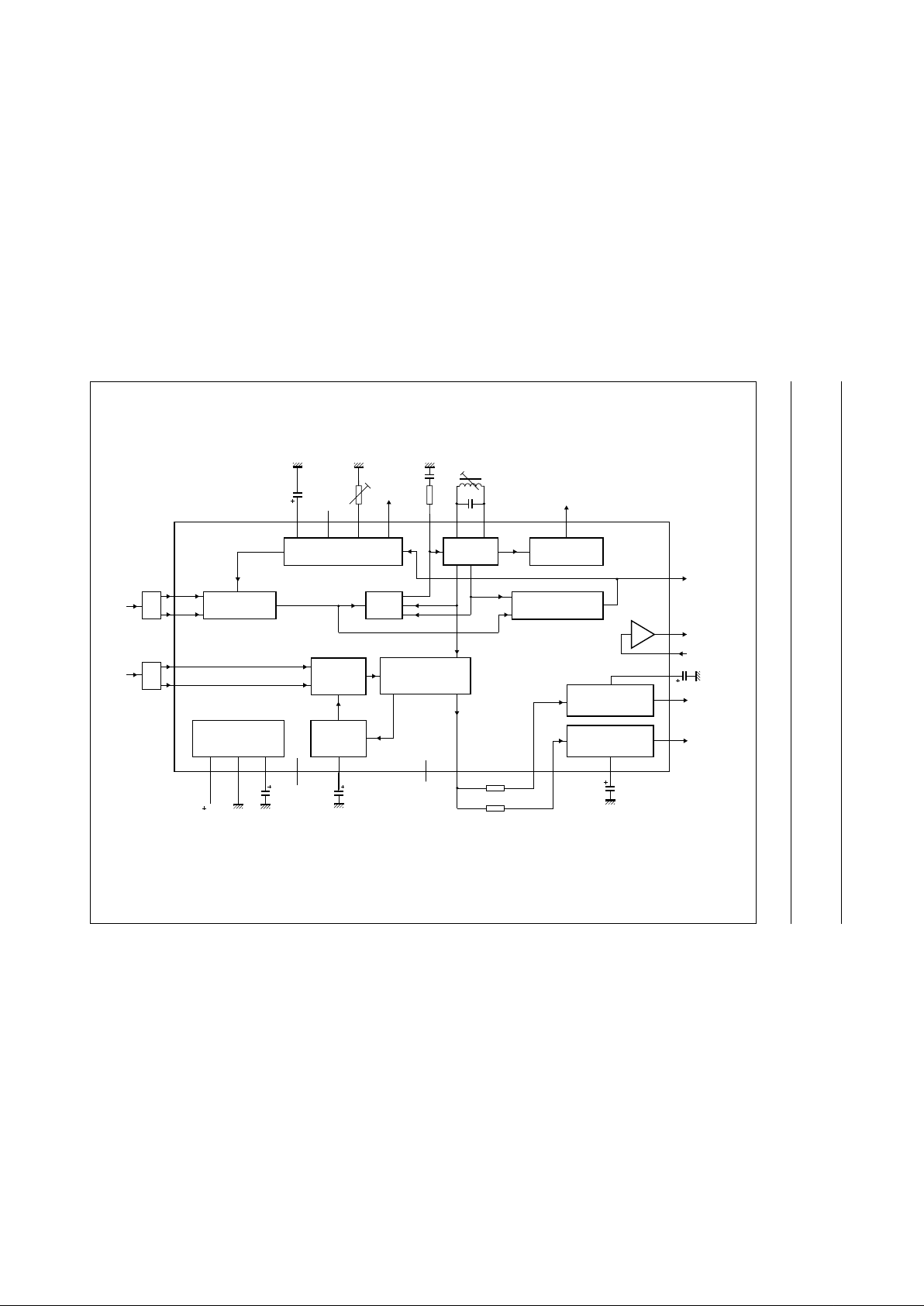
BLOCK DIAGRAM
handbook, full pagewidth
SINGLE REFERENCE
MIXER
VCO TWD
AFC DETECTOR
TUNER AND VIF-AGC
FPLL
VIDEO DEMODULATOR
AND AMPLIFIER
SIF
AMPLIFIER
SIF-AGC
INTERNAL VOLTAGE
STABILIZER
FM DETECTOR (PLL)
AF AMPLIFIER
VIF AMPLIFIER
SIF
VIF
TDA9813T
26 24 23 7 6
8
18
19
13
10
11
20212251625 43
2
1
28
27
5 V
VP1/2
C
AGC
917 15
5.5
5.74
SIF
14 12
n.c.n.c.
AF2
FM DETECTOR (PLL)
AF AMPLIFIER
AF1
VIDEO
BUFFER
V
i(vid)
CVBS
2 V (p-p)
video
1 V (p-p)
AFC
2 x f
PC
tuner
AGC
loop
filter
n.c.
TOP
C
AGC
MHA037
Fig.1 Block diagram.
1999 Sep 16 5
Philips Semiconductors Product specification
VIF-PLL with QSS-IF and
dual FM-PLL demodulator
TDA9813T
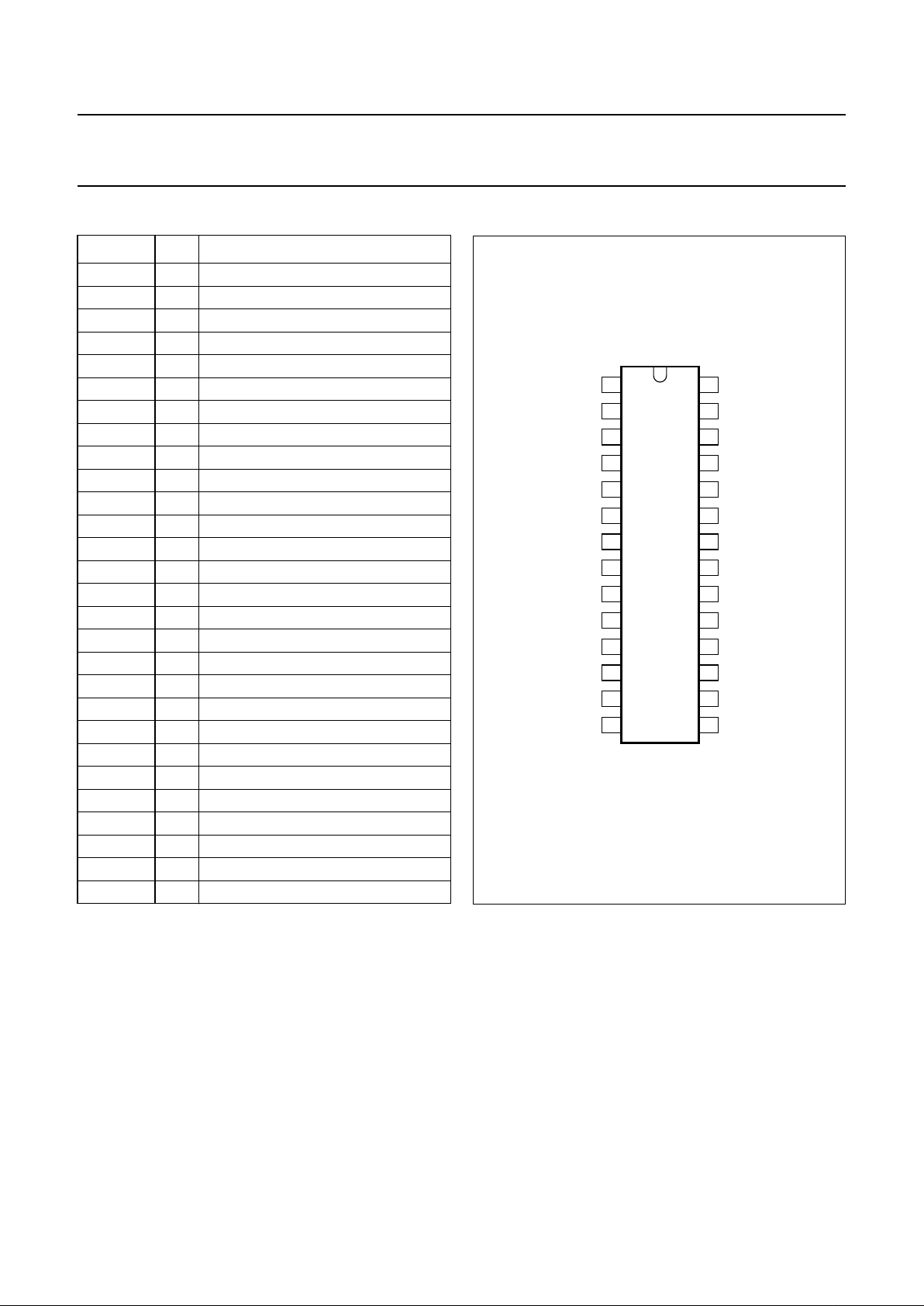
PINNING
SYMBOL PIN DESCRIPTION
V
i VIF1
1 VIF differential input signal voltage 1
V
i VIF2
2 VIF differential input signal voltage 2
n.c. 3 not connected
TADJ 4 tuner AGC takeover adjust (TOP)
T
PLL
5 PLL loop filter
C
SAGC
6 SIF-AGC capacitor
n.c. 7 not connected
V
o CVBS
8 CVBS output signal voltage
n.c. 9 not connected
V
o AF1
10 audio voltage frequency output 1
V
o AF2
11 audio voltage frequency output 2
C
DEC2
12 decoupling capacitor 2
C
DEC1
13 decoupling capacitor 1
V
i FM2
14 sound intercarrier input voltage 2
V
i FM1
15 sound intercarrier input voltage 1
TAGC 16 tuner AGC output
V
o QSS
17 single reference QSS output voltage
V
o(vid)
18 composite video output voltage
V
i(vid)
19 video buffer input voltage
AFC 20 AFC output
VCO1 21 VCO1 reference circuit for 2f
PC
VCO2 22 VCO2 reference circuit for 2f
PC
C
ref
231⁄2VPreference capacitor
GND 24 ground
C
VAGC
25 VIF-AGC capacitor
V
P
26 supply voltage
V
i SIF1
27 SIF differential input signal voltage 1
V
i SIF2
28 SIF differential input signal voltage 2
Fig.2 Pin configuration.
handbook, halfpage
TDA9813T
MHA038
1
2
3
4
5
6
7
8
9
10
11
12
13
14
V
V
n.c.
TADJ
T
C
n.c.
V
n.c.
V
i FM2
28
27
26
25
24
23
22
21
20
19
18
17
16
15
V
V
V
C
GND
C
VCO2
VCO1
AFC
V
V
V
TAGC
V
o CVBS
SAGC
PLL
i VIF2
i VIF1
P
i SIF1
i SIF2
VAGC
ref
i FM1
o QSS
o(vid)
i(vid)
C
DEC1
C
DEC2
V
o AF2
V
o AF1

1999 Sep 16 6
Philips Semiconductors Product specification
VIF-PLL with QSS-IF and
dual FM-PLL demodulator
TDA9813T
FUNCTIONAL DESCRIPTION
The integrated circuit comprises the functional blocks as
shown in Fig.1:
• Vision IF amplifier
• Tuner and VIF-AGC
• Frequency Phase Locked Loop (FPLL) detector
• VCO, Travelling Wave Divider (TWD) and AFC
• Video demodulator and amplifier
• Video buffer
• SIF amplifier and SIF-AGC
• Single reference Quasi Split Sound (QSS) mixer
• FM-PLL demodulator
• Internal voltage stabilizer and1⁄2VPreference.
Vision IF amplifier
The vision IF amplifier consists of three AC-coupled
differential amplifier stages. Each differential stage
comprises a feedback network controlled by emitter
degeneration.
Tuner and VIF-AGC
The AGC capacitor voltage is transferred to an internal IF
control signal, and is fed to the tuner AGC to generate the
tuner AGC output current (open-collector output).
The tuner AGC takeover point can be adjusted. This
allows the tuner and the SAW filter to be matched to
achieve the optimum IF input level.
The AGC detector charges/discharges the AGC capacitor
to the required voltage for setting of VIF and tuner gain in
order to keep the video signal at a constant level.
Therefore the sync level of the video signal is detected.
Frequency Phase Locked Loop (FPLL) detector
The VIF amplifier output signal is fed into a frequency
detector and into a phase detector via a limiting amplifier.
During acquisition the frequency detector produces a DC
current proportional to the frequency difference between
the input and the VCO signal. After frequency lock-in the
phase detector produces a DC current proportional to the
phase difference between the VCO and the input signal.
The DC current of either frequency detector or phase
detector is converted into a DC voltage via the loop filter,
which controls the VCO frequency.
VCO, Travelling Wave Divider (TWD) and AFC
The VCO operates with a resonance circuit (with L and C
in parallel) at double the PC frequency. The VCO is
controlled by two integrated variable capacitors.
The control voltage required to tune the VCO from its
free-running frequency to actually double the PC
frequency is generated by the frequency-phase detector
(FPLL) and fed via the loop filter to the first variable
capacitor.Thiscontrol voltage is amplified and additionally
converted into a current which represents the AFC output
signal.AtcentrefrequencytheAFCoutputcurrentisequal
to zero.
The oscillator signal is divided-by-two with a TWD which
generates two differential output signals with a 90 degree
phase difference independent of the frequency.
Video demodulator and amplifier
The video demodulator is realized by a multiplier which is
designedfor low distortion and largebandwidth.The vision
IF input signal is multiplied with the ‘in phase’ signal of the
travelling wave divider output.
The demodulator output signal is fed via an integrated
low-pass filter for attenuation of the carrier harmonics to
the video amplifier. The video amplifier is realized by an
operational amplifier with internal feedback and high
bandwidth. A low-pass filter is integrated to achieve an
attenuation of the carrier harmonics. The video output
signal is 1 V (p-p) for nominal vision IF modulation.
Video buffer
For an easy adaption of the sound traps an operational
amplifier with internal feedback is used. This amplifier is
featured with a high bandwidth and 7 dB gain. The input
impedance is adapted for operating in combination with
ceramic sound traps. The output stage delivers a nominal
2 V (p-p) positive video signal. Noise clipping is provided.
SIF amplifier and SIF-AGC
The sound IF amplifier consists of two AC-coupled
differential amplifier stages. Each differential stage
comprises a controlled feedback network provided by
emitter degeneration.
The SIF-AGC detector is related to the SIF input signals
(average level of FM carriers) and controls the SIF
amplifier to provide a constant SIF signal to the single
reference QSS mixer.

1999 Sep 16 7
Philips Semiconductors Product specification
VIF-PLL with QSS-IF and
dual FM-PLL demodulator
TDA9813T
Single reference QSS mixer
The single reference QSS mixer is realized by a multiplier.
The SIF amplifier output signal is fed to the single
reference QSS mixer and converted to intercarrier
frequency by the regenerated picture carrier (VCO).
The mixer output signal is fed via a high-pass for
attenuation of the video signal components to the output
pin 17. With this system a high performance hi-fi stereo
sound processing can be achieved.
FM-PLL demodulator
Each FM-PLL demodulator consists of a limiter, an
FM-PLL and an AF amplifier. The limiter provides the
amplification and limitation of the FM sound intercarrier
signal before demodulation. The result is high sensitivity
and AM suppression. The amplifier consists of 7 stages
which are internally AC-coupled in order to minimize the
DC offset and to save pins for DC decoupling.
The second limiter is extended with an additional level
detector consisting of a rectifier and a comparator.
By means of this the AF2 signal is set to mute and the
PLL VCO is switched off, if the intercarrier signal at pin 14
is below 1 mV (RMS) in order to avoid false identification
of a stereo decoder. It should be noted that noise at pin 14
disables the mute state (at low SIF input signal), but this
willnot lead to false identification.This‘auto-mute’ function
can be disabled by connecting a 5.6 kΩ resistor from
pin 14 to VP (see Fig.11).
Furthermore the AF output signals can be muted by
connecting a resistor between the limiter inputs pin 14 or
pin 15 and ground.
TheFM-PLLconsists of an integrated relaxation oscillator,
an integrated loop filter and a phase detector.
The oscillatorislockedtotheFMintercarriersignal,output
from the limiter. As a result of locking, the oscillator
frequency tracks with the modulation of the input signal
and the oscillator control voltage is superimposed by the
AF voltage. The FM-PLL operates as an FM demodulator.
The AF amplifier consists of two parts:
1. The AF preamplifier for FM sound is an operational
amplifier with internal feedback, high gain and high
common mode rejection. The AF voltage from the PLL
demodulator, by principle a small output signal, is
amplified by approximately 33 dB. The low-pass
characteristicof the amplifierreducesthe harmonics of
the intercarrier signal at the sound output terminal.
An additionalDC control circuitisimplemented to keep
the DC level constant, independent of process spread.
2. The AF output amplifier (10 dB) provides the required
output level by a rail-to-rail output stage. This amplifier
makes use of an input selector for switching to FM or
mute state, controlled by the mute switching voltage.
Internal voltage stabilizer and
1
⁄2VPreference
The band gap circuit internally generates a voltage of
approximately 1.25 V, independent of supply voltage and
temperature. A voltage regulator circuit, connected to this
voltage, produces a constant voltage of 3.6 V which is
used as an internal reference voltage.
For all audio output signals the constant reference voltage
cannot be used because large output signals are required.
Therefore these signals refer to half the supply voltage to
achieve a symmetrical headroom, especially for the
rail-to-rail output stage. For ripple and noise attenuation
the
1
⁄2VP voltage has to be filtered via a low-pass filter by
using an external capacitor together with an integrated
resistor (fg= 5 Hz). For a fast setting to 1⁄2VP an internal
start-up circuit is added.

1999 Sep 16 8
Philips Semiconductors Product specification
VIF-PLL with QSS-IF and
dual FM-PLL demodulator
TDA9813T
LIMITING VALUES
In accordance with the Absolute Maximum Rating System (IEC 134).
Notes
1. IP= 125 mA; T
amb
=70°C; R
th(j-a)
= 80 K/W.
2. Machine model class B (L = 2.5 µH).
THERMAL CHARACTERISTICS
SYMBOL PARAMETER CONDITIONS MIN. MAX. UNIT
V
P
supply voltage (pin 26) maximum chip temperature
of 125 °C; note 1
0 5.5 V
V
n
voltage at pins 1 to 7, 9 to 16, 19, 20 and
23 to 28
0V
P
V
t
s(max)
maximum short-circuit time − 10 s
V
16
tuner AGC output voltage 0 13.2 V
T
stg
storage temperature −25 +150 °C
T
amb
ambient temperature −20 +70 °C
V
es
electrostatic handling voltage note 2 −300 +300 V
SYMBOL PARAMETER CONDITIONS VALUE UNIT
R
th(j-a)
thermal resistance from junction to ambient in free air 80 K/W
1999 Sep 16 9
Philips Semiconductors Product specification
VIF-PLL with QSS-IF and
dual FM-PLL demodulator
TDA9813T
CHARACTERISTICS
VP=5V; T
amb
=25°C; see Table 1 for input frequencies and carrier ratios (B/G standard); input level
V
i IF 1-2
= 10 mV RMS value (sync-level); video modulation DSB; residual carrier: 10%; video signal in accordance with
“CCIR, line 17”
; measurements taken in Fig.11; unless otherwise specified.
SYMBOL PARAMETER CONDITIONS MIN. TYP. MAX. UNIT
Supply (pin 26)
V
P
supply voltage note 1 4.5 5 5.5 V
I
P
supply current 93 109 125 mA
Vision IF amplifier (pins 1 and 2)
V
i VIF(rms)
input signal voltage
sensitivity (RMS value)
−1 dB video at output − 60 100 µV
V
i max(rms)
maximum input signal
voltage (RMS value)
+1 dB video at output 120 200 − mV
∆V
o(int)
internal IF amplitude
difference between picture
and sound carrier
within AGC range;
∆f = 5.5 MHz
− 0.7 1 dB
G
IFcr
IF gain control range see Fig.3 65 70 − dB
R
i(diff)
differential input resistance note 2 1.7 2.2 2.7 kΩ
C
i(diff)
differential input capacitance note 2 1.2 1.7 2.5 pF
V
1,2
DC input voltage note 2 − 3.4 − V
True synchronous video demodulator; note 3
f
VCO(max)
maximum oscillator
frequency for carrier
regeneration
f=2f
PC
125 130 − MHz
∆f
osc
/∆T oscillator drift as a function
of temperature
oscillator is free-running;
I
AFC
= 0; note 4
−−±20 × 10−6K
−1
V
o ref(rms)
oscillator voltage swing at
pins 21 and 22 (RMS value)
70 100 130 mV
f
PC CR
picture carrier capture range ±1.4 ±1.8 − MHz
t
acq
acquisition time BL = 75 kHz; note 5 −−30 ms
V
i VIF(rms)
VIF input signal voltage
sensitivity for PLL to be
locked (RMS value; pins 1
and 2)
maximum IF gain; note 6 − 30 70 µV
Composite video amplifier (pin 18; sound carrier off)
V
o video(p-p)
output signal voltage
(peak-to-peak value)
see Fig.8 0.88 1.0 1.12 V
V/S ratio between video
(black-to-white) and
sync level
1.9 2.33 3.0 −
V
18(sync)
sync voltage level − 1.5 − V
V
18(clu)
upper video clipping voltage
level
VP− 1.1 VP− 1 − V

1999 Sep 16 10
Philips Semiconductors Product specification
VIF-PLL with QSS-IF and
dual FM-PLL demodulator
TDA9813T
V
18(cll)
lower video clipping voltage
level
− 0.7 0.9 V
R
o,18
output resistance note 2 −−10 Ω
I
int 18
internal DC bias current for
emitter-follower
2.2 3.0 − mA
I
18 max(sink)
maximum AC and DC output
sink current
1.6 −− mA
I
18 max(source)
maximum AC and DC output
source current
2.9 −− mA
B
−1
−1 dB video bandwidth CL< 50 pF; RL>1kΩ;
AC load
56− MHz
B
−3
−3 dB video bandwidth CL< 50 pF; RL>1kΩ;
AC load
78− MHz
α
H(sup)
suppression of video signal
harmonics
CL< 50 pF; RL>1kΩ;
AC load; note 7a
35 40 − dB
PSRR power supply ripplerejection
at pin 18
video signal; grey level;
see Fig.9
32 35 − dB
CVBS buffer amplifier (only) and noise clipper (pins 8 and 19)
R
i,19
input resistance note 2 2.6 3.3 4.0 kΩ
C
i,19
input capacitance note 2 1.4 2 3.0 pF
V
I,19
DC input voltage 1.4 1.7 2.0 V
G
v
voltage gain note 8 6.5 7 7.5 dB
V
8(clu)
upper video clipping voltage
level
3.9 4.0 − V
V
8(cll)
lower video clipping voltage
level
− 1.0 1.1 V
R
o,8
output resistance note 2 −−10 Ω
I
int 8
DC internal bias current for
emitter-follower
2.0 2.5 − mA
I
o,8 max(sink)
maximum AC and DC output
sink current
1.4 −− mA
I
o,10 max(source)
maximum AC and DC output
source current
2.4 −− mA
B
−1
−1 dB video bandwidth CL< 20 pF; RL>1kΩ;
AC load
8.4 11 − MHz
B
−3
−3 dB video bandwidth CL< 20 pF; RL>1kΩ;
AC load
11 14 − MHz
Measurements from IF input to CVBS output (pin 8; 330 Ω between pins 18 and 19, sound carrier off)
V
o CVBS(p-p)
CVBS output signal voltage
on pin 8
(peak-to-peak value)
note 8 1.7 2.0 2.3 V
V
o CVBS(sync)
sync voltage level − 1.35 − V
SYMBOL PARAMETER CONDITIONS MIN. TYP. MAX. UNIT
 Loading...