

Philips TDA9812T, TDA9812 Datasheet

INTEGRATED CIRCUITS
DATA SH EET
TDA9812
Multistandard VIF-PLL and
FM-PLL/AM demodulator
Preliminary specification
File under Integrated Circuits, IC02
Philips Semiconductors
1995 Mar 21

Philips Semiconductors Preliminary specification
Multistandard VIF-PLL and
FM-PLL/AM demodulator
FEATURES
• 5 V positive supply voltage
• Gain controlled wide band VIF-amplifier (AC-coupled)
• True synchronous demodulation with active carrier
regeneration (very linear demodulation, good
intermodulation figures, reduced harmonics, excellent
pulse response)
• Gated phase detector for L/L accent standard
• VCO frequency switchable between L and L accent
(alignment external) picture carrier frequency
• Separate video amplifier for sound trap buffering with
high video bandwidth
• VIF AGC detector for gain control, operating as peak
sync detector for B/G (optional external AGC) and peak
white detector for L; signal controlled reaction time for L
• Tuner AGC with adjustable Take Over Point (TOP)
• AFC detector without extra reference circuit
• AC-coupled limiter amplifier for sound intercarrier signal
• Alignment-free FM-PLL demodulator with high linearity,
switchable de-emphasis for FM
• AM-SIF AGC detector for gain controlled SIF amplifier
• AM demodulator without extra reference circuit
• Stabilizer circuit for ripple rejection and to achieve
constant output signals.
TDA9812
GENERAL DESCRIPTION
The TDA9812/T is an integrated circuit for multistandard
vision IF signal processing and AM and FM sound
demodulation in TV and VTR sets.
ORDERING INFORMATION
TYPE
NUMBER
TDA9812 SDIP32 plastic shrink dual in-line package; 32 leads (400 mil) SOT232-1
TDA9812T SO28 plastic small outline package; 28 leads body width 7.5 mm SOT136-1
1995 Mar 21 2
NAME DESCRIPTION VERSION
PACKAGE

Philips Semiconductors Preliminary specification
Multistandard VIF-PLL and
TDA9812
FM-PLL/AM demodulator
QUICK REFERENCE DATA
SYMBOL PARAMETER CONDITIONS MIN. TYP. MAX. UNIT
V
P
I
P
V
i VIF(rms)
V
o CVBS(p-p)
B
−3
S/N(W) weighted signal-to-noise ratio for
IM
α1.1
IM
α3.3
α
H(sup)
V
i SIF(rms)
V
o(rms)
THD total harmonic distortion 54% modulation
S/N (W) weighted signal-to-noise ratio 54% modulation
supply voltage 4.5 5 5.5 V
supply current 82 96 110 mA
vision IF input signal voltage
−1 dB video at output − 60 100 µV
sensitivity (RMS value)
CVBS output signal voltage
1.7 2.0 2.3 V
(peak-to-peak value)
−3 dB video bandwidth on pin CVBS B/G and L standard;
< 20 pF; RL> 1kΩ;
C
L
78−MHz
AC load
56 60 − dB
video
intermodulation attenuation at ‘blue’ f = 1.1 MHz 58 64 − dB
intermodulation attenuation at ‘blue’ f = 3.3 MHz 58 64 − dB
suppression of harmonics in video
35 40 − dB
signal
sound IF input signal voltage
−3 dB video at AF output − 70 100 µV
sensitivity (RMS value)
audio output signal voltage for FM
(RMS value)
audio output signal voltage for AM
B/G standard;
− 0.5 − V
54% modulation
L standard; 54% modulation − 0.5 − V
(RMS value)
FM − 0.15 0.5 %
AM − 0.5 1.0 %
FM − 60 − dB
AM 47 53 − dB
1995 Mar 21 3
Philips Semiconductors Preliminary specification
Multistandard VIF-PLL and
FM-PLL/AM demodulator
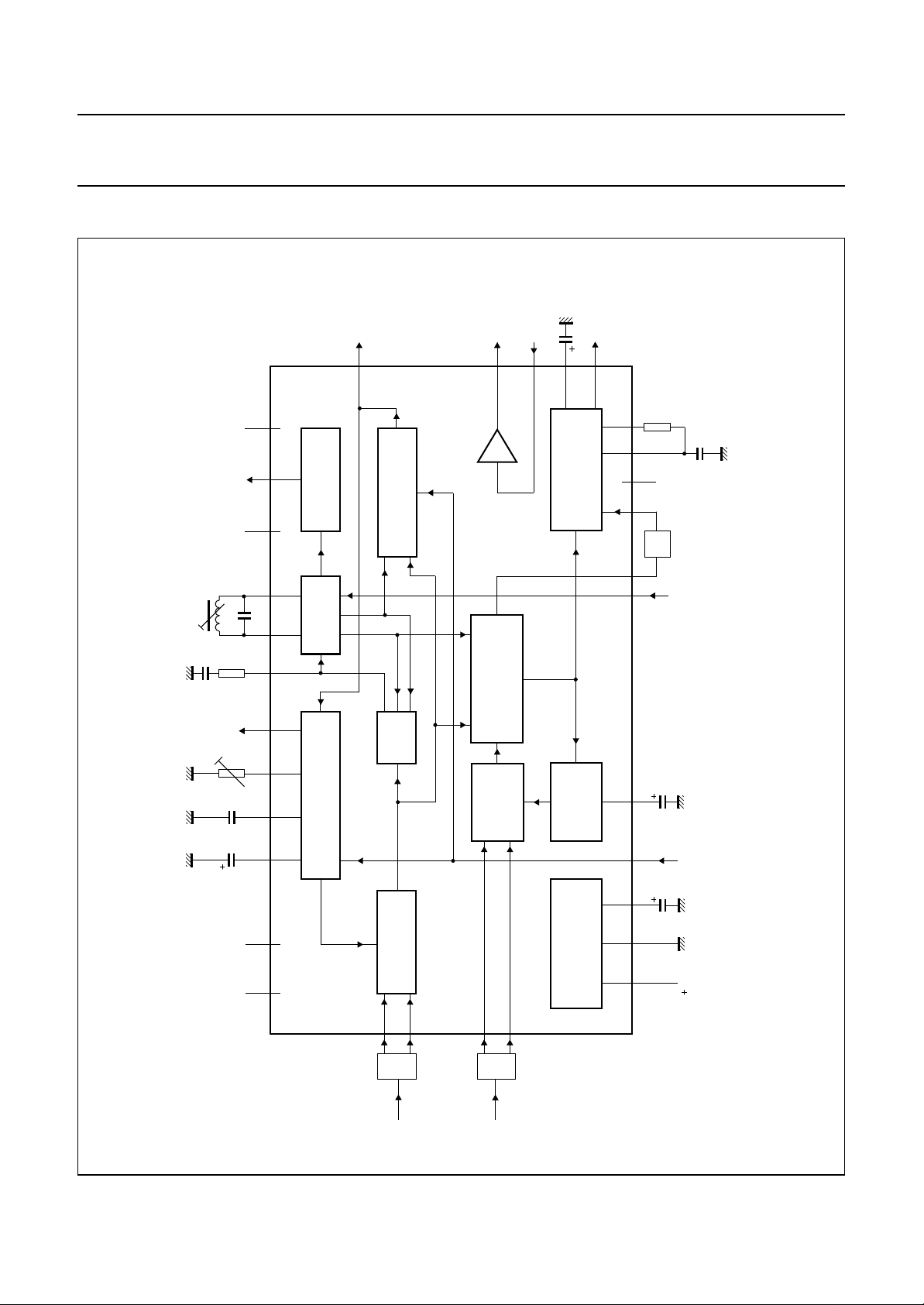
BLOCK DIAGRAM
3018
n.c.n.c.n.c. n.c.
AFC
23
(20)
filter
VCO1
VCO2
24
(21)
25
(22)
7
(5)
19
(16)
6
(4)
3
(3)
28
(25)
54
handbook, full pagewidth
PLL
T
TADJ
PC
2 x f
TAGC
TOP
loop
tuner
BL
C
AGC
C
AGC
o (vid)
V
video
1 V (p-p)
21 (18)
AFC DETECTOR
VCO TWD
TUNER AND VIF-AGC
AND AMPLIFIER
VIDEO DEMODULATOR
FPLL
VIF AMPLIFIER
CVBS
2 V (p-p)
10 (8)
VIDEO
BUFFER
TDA9812
MIXER AND
INTERCARRIER
AM DEMODULATOR
SIF
AMPLIFIER
(vid)
Vi
15 (13)
22 (19)
FM DETECTOR (PLL)
SIF-AGC
INTERNAL VOLTAGE
o AF
V
AF/AM
(11)
(12)
(14)
(15)
(17)
(9)
(6)
(7)
(23)
(24)
(26)
13
14
16
17
20
11
8
9
26
27
29
MBE452
P
V
1/2
12 (10)
AF AMPLIFIER
STABILIZER
de-emphasis
n.c.
iFM
V
o(int)
5.5
SIF
V
L/L
switch
SAGC
C
switch
standard
ref
C
GND
P
5 V
V
TDA9812
O
DEEM
I
DEEM
STD
Fig.1 Block diagram (TDA9812T pinning in parenthesis).
2 (2)
1 (1)
VIF
i VIF1
i VIF2
V
V
1995 Mar 21 4
32 (28)
31 (27)
SIF
i SIF2Vi SIF1
V

Philips Semiconductors Preliminary specification
Multistandard VIF-PLL and
FM-PLL/AM demodulator
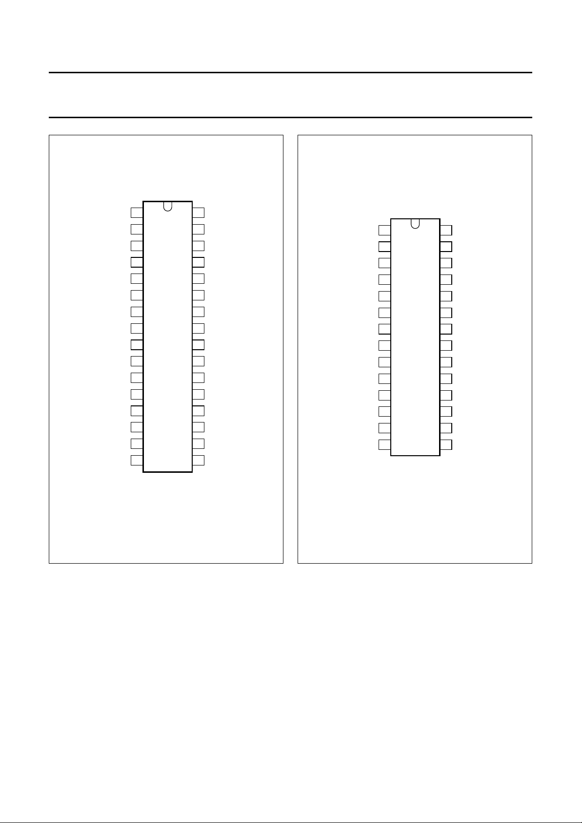
PINNING
SYMBOL PIN SDIP32 PIN SO28 DESCRIPTION
V
i VIF1
V
i VIF2
C
BL
n.c. 4 − not connected
n.c. 5 − not connected
TADJ 6 4 tuner AGC take-over adjust (TOP)
T
PLL
C
SAGC
STD 9 7 standard switch
V
o CVBS
LSWI 11 9 L/L accent switch
V
oAF
DEEM
I
DEEM
O
C
DEC
n.c. 16 14 not connected
V
iFM
n.c. 18 − not connected
TAGC 19 16 tuner AGC output
V
o(int)
V
o(vid)
V
i(vid)
AFC 23 20 AFC output
VCO1 24 21 VCO1 reference circuit for 2f
VCO2 25 22 VCO2 reference circuit for 2f
C
ref
GND 27 24 ground
C
VAGC
V
P
n.c. 30 − not connected
V
i SIF1
V
i SIF2
1 1 VIF differential input signal voltage 1
2 2 VIF differential input signal voltage 2
3 3 black level detector
7 5 PLL loop filter
8 6 SIF AGC capacitor
10 8 CVBS output signal voltage
12 10 audio voltage frequency output
13 11 de-emphasis input
14 12 de-emphasis output
15 13 decoupling capacitor
17 15 sound intercarrier input voltage
20 17 sound intercarrier output voltage
21 18 composite video output voltage
22 19 video buffer input voltage
PC
PC
26 23
1
⁄2VP reference capacitor
28 25 VIF AGC capacitor
29 26 supply voltage
31 27 SIF differential input signal voltage 1
32 28 SIF differential input signal voltage 2
TDA9812
1995 Mar 21 5
Philips Semiconductors Preliminary specification
Multistandard VIF-PLL and
FM-PLL/AM demodulator
handbook, halfpage
V
V
C
SAGC
V
o CVBS
V
DEEM
DEEM
C
i VIF1
i VIF2
C
BL
n.c.
n.c.
TADJ
T
PLL
STD
LSWI
o AF
DEC
n.c.
1
2
3
4
5
6
7
8
TDA9812
9
10
11
12
13
I
14
O
15
16
32
31
30
29
28
27
26
25
24
23
22
21
20
19
18
17
MBE436
V
i SIF2
V
i SIF1
n.c.
V
P
C
VAGC
GND
C
ref
VCO2
VCO1
AFC
V
i(vid)
V
o(vid)
V
o(int)
TAGC
n.c.
V
i FM
handbook, halfpage
V
i VIF1
V
i VIF2
C
SAGC
V
o CVBS
V
DEEM
DEEM
C
C
BL
TADJ
T
PLL
STD
LSWI
o AF
DEC
n.c.
I
O
1
2
3
4
5
6
7
TDA9812T
8
9
10
11
12
13
14
MBE435
TDA9812
V
28
i SIF2
V
27
i SIF1
V
26
P
C
25
VAGC
24
GND
C
23
ref
22
VCO2
21
VCO1
20
AFC
V
19
i(vid)
V
18
o(vid)
V
17
o(int)
16
TAGC
V
15
i FM
Fig.2 Pin configuration (SDIP32).
1995 Mar 21 6
Fig.3 Pin configuration (SO28).

Philips Semiconductors Preliminary specification
Multistandard VIF-PLL and
FM-PLL/AM demodulator
FUNCTIONAL DESCRIPTION
Vision IF amplifier
The vision IF amplifier consists of three AC-coupled
differential amplifier stages. Each differential stage
comprises a feedback network controlled by emitter
degeneration.
Tuner and VIF AGC
The AGC capacitor voltage is transferred to an internal IF
control signal, and is fed to the tuner AGC to generate the
tuner AGC output current (open-collector output). The
tuner AGC take-over point can be adjusted. This allows the
tuner and the SWIF filter to be matched to achieve the
optimum IF input level.
The AGC detector charges/discharges the AGC capacitor
to the required voltage for setting of VIF and tuner gain in
order to keep the video signal at a constant level.
Therefore for negative video modulation the sync level and
for positive video modulation the peak white level of the
video signal is detected. In order to reduce the reaction
time for positive modulation, where a very large time
constant is needed, an additional level detector increases
the discharging current of the AGC capacitor (fast mode)
in the event of a decreasing VIF amplitude step. The
additional level information is given by the black-level
detector voltage.
Frequency-Phase detector (FPLL)
The VIF-amplifier output signal is fed into a frequency
detector and into a phase detector via a limiting amplifier.
During acquisition the frequency detector produces a DC
current proportional to the frequency difference between
the input and the VCO signal. After frequency lock-in the
phase detector produces a DC current proportional to the
phase difference between the VCO and the input signal.
The DC current of either frequency detector or phase
detector is converted into a DC voltage via the loop filter,
which controls the VCO frequency. In the event of positive
modulated signals the phase detector is gated by
composite sync in order to avoid signal distortion for
overmodulated VIF signals.
TDA9812
VCO, travelling wave divider and AFC
The VCO operates with a resonance circuit (with L and C
in parallel) at double the PC frequency. The VCO is
controlled by two integrated variable capacitors. The
control voltage required to tune the VCO from its freerunning frequency to actually double the PC frequency is
generated by the Frequency-Phase detector and fed via
the loop filter to the first variable capacitor (FPLL). This
control voltage is amplified and additionally converted into
a current which represents the AFC output signal. The
VCO centre frequency can be decreased (required for
L/L accent standard) by activating an additional internal
capacitor. This is achieved by using the L/L accent switch.
In this event the second variable capacitor can be
controlled by a variable resistor at the L/L accent switch for
setting the VCO centre frequency to the required
L/L accent value. At centre frequency the AFC output
current is equal to zero.
The oscillator signal is divided-by-two with a Travelling
Wave Divider (TWD) which generates two differential
output signals with a 90 degree phase difference
independent of the frequency.
Video demodulator and amplifier
The video demodulator is realized by a multiplier which is
designed for low distortion and large bandwidth. The vision
IF input signal is multiplied with the ‘in phase’ signal of the
travelling wave divider output. In the demodulator stage
the video signal polarity can be switched in accordance
with the TV standard.
The demodulator output signal is fed via an integrated
low-pass filter for attenuation of the carrier harmonics to
the video amplifier. The video amplifier is realized by an
operational amplifier with internal feedback and high
bandwidth. A low-pass filter is integrated to achieve an
attenuation of the carrier harmonics for B/G and
L standard. The standard dependent level shift in this
stage delivers the same sync level for positive and
negative modulation. The video output signal is 1 V (p-p)
for nominal vision IF modulation.
1995 Mar 21 7

Philips Semiconductors Preliminary specification
Multistandard VIF-PLL and
FM-PLL/AM demodulator
Video buffer
For an easy adaption of the sound traps an operational
amplifier with internal feedback is used in the event of B/G
and L standard. This amplifier is featured with a high
bandwidth and 7 dB gain. The input impedance is adapted
for operating in combination with ceramic sound traps. The
output stage delivers a nominal 2 V (p-p) positive video
signal. Noise clipping is provided.
SIF amplifier and AGC for AM sound
The sound IF amplifier consists of two AC-coupled
differential amplifier stages. Each differential stage
comprises a controlled feedback network provided by
emitter degeneration.
The SIF AGC detector is related to the SIF input signals
(average level of AM carrier) and controls the SIF amplifier
to provide a constant SIF signal to the AM demodulator.
The SIF AGC reaction time is set to ‘slow’ for nominal
video conditions. But with a decreasing VIF amplitude step
the SIF AGC is set to ‘fast’ mode controlled by the VIF
AGC detector.
Intercarrier mixer
The intercarrier mixer is realized by a multiplier. The VIF
amplifier output signal is fed to the intercarrier mixer and
converted to intercarrier frequency by the regenerated
picture carrier (VCO). The mixer output signal is fed via a
high-pass for attenuation of the video signal components.
AM demodulator
The AM demodulator is realized by a multiplier. The
modulated SIF amplifier output signal is multiplied in
phase with the limited (AM is removed) SIF amplifier
output signal. The demodulator output signal is fed via an
integrated low-pass filter for attenuation of the carrier
harmonics to the AF amplifier.
FM detector
The FM detector consists of a limiter, an FM-PLL and an
AF amplifier. The limiter provides the amplification and
limitation of the FM sound intercarrier signal before
demodulation. The result is high sensitivity and AM
suppression. The amplifier consists of 7 stages which are
internally AC-coupled in order to minimize the DC offset
and to save pins for DC decoupling.
TDA9812
The FM-PLL consists of an integrated relaxation oscillator,
an integrated loop filter and a phase detector. The
oscillator is locked to the FM intercarrier signal, output
from the limiter. As a result of locking, the oscillator
frequency tracks with the modulation of the input signal
and the oscillator control voltage is superimposed by the
AF voltage. The FM-PLL operates as an FM-demodulator
The AF amplifier consists of two parts:
• The AF preamplifier for FM sound is an operational
amplifier with internal feedback, high gain and high
common mode rejection. The AF voltage from the PLL
demodulator, by principle a small output signal, is
amplified by approximately 33 dB. The low-pass
characteristic of the amplifier reduces the harmonics of
the intercarrier signal at the sound output terminal, at
which the de-emphasis network for FM sound is applied.
An additional DC control circuit is implemented to keep
the DC level constant, independent of process spread.
• The AF output amplifier (10 dB) provides the required
output level by a rail-to-rail output stage. This amplifier
makes use of an input selector for switching to AM, FM
de-emphasis or mute state, controlled by the standard
switching voltage and the mute switching voltage.
1
Internal voltage stabilizer and
The bandgap circuit internally generates a voltage of
approximately 1.25 V, independent of supply voltage and
temperature. A voltage regulator circuit, connected to this
voltage, produces a constant voltage of 3.6 V which is
used as an internal reference voltage.
For all audio output signals the constant reference voltage
cannot be used because large output signals are required.
Therefore these signals refer to half the supply voltage to
achieve a symmetrical headroom, especially for the
rail-to-rail output stage. For ripple and noise attenuation
1
the
⁄2VP voltage has to be filtered via a low-pass filter by
using an external capacitor together with an integrated
resistor (fg= 5 Hz). For a fast setting to 1⁄2VP an internal
start-up circuit is added.
⁄2VP-reference
1995 Mar 21 8

Philips Semiconductors Preliminary specification
Multistandard VIF-PLL and
TDA9812
FM-PLL/AM demodulator
LIMITING VALUES
SDIP32
In accordance with the Absolute Maximum Rating System (IEC 134).
SYMBOL PARAMETER CONDITIONS MIN. MAX. UNIT
V
P
supply voltage (pin 29) maximum chip temperature
of +120 °C; note 1
V
i
voltage at pins 1 to 9, 11 to 19,
22, 23 and 28 to 32
t
s(max)
V
19
T
stg
T
amb
V
esd
maximum short-circuit time − 10 s
tuner AGC output voltage 0 13.2 V
storage temperature −25 +150 °C
operating ambient temperature −20 +70 °C
electrostatic handling voltage note 2 −300 +300 V
Notes
1. I
= 110 mA; T
P
= +70 °C; R
amb
= 60 K/W for SDIP32 and R
th j-a
= 80 K/W for SO28.
th j-a
2. Charge device model class B: equivalent to discharging a 200 pF capacitor via a 0 Ω series resistor.
0 5.5 V
0V
P
V
THERMAL CHARACTERISTICS
SYMBOL PARAMETER VALUE UNIT
R
th j-a
thermal resistance from junction to ambient in free air
SDIP32 60 K/W
SO28 80 K/W
1995 Mar 21 9

Philips Semiconductors Preliminary specification
Multistandard VIF-PLL and
TDA9812
FM-PLL/AM demodulator
CHARACTERISTICS
SDIP32 pinning; VP=5V; T
RMS value (sync-level for B/G, peak white level for L); video modulation DSB; residual carrier B/G: 10%; L = 3%;
video signal in accordance with
SYMBOL PARAMETER CONDITIONS MIN. TYP. MAX. UNIT
Supply (pin 29)
V
P
I
P
supply voltage note 1 4.5 5 5.5 V
supply current 82 96 110 mA
Vision IF amplifier (pins 1 and 2)
V
i(VIF)(rms)
input signal voltage sensitivity
(RMS value)
V
i(max)(rms)
maximum input signal voltage
(RMS value)
∆V
o(int)
internal IF amplitude difference
between picture and sound
carrier
G
R
C
V
IF
i(diff)
i(diff)
1/2
IF gain control range see Figs 5 and 6 65 70 − dB
differential input resistance note 2 1.7 2.2 2.7 kΩ
differential input capacitance note 2 1.2 1.7 2.5 pF
DC input voltage − 3.4 − V
True synchronous video demodulator; see note 3
f
VCO(max)
maximum oscillator frequency
for carrier regeneration
∆f
VCO
oscillator drift (free-running) as a
function of temperature
V
0 ref(rms)
oscillator voltage swing at
pins 24 and 25 (RMS value)
∆f
pc(capt)
vision carrier capture frequency
range
∆f
pc(ff)
vision carrier frequency
(free-running) accuracy
∆f
pc(alg)
L/L accent alignment frequency
range
t
acqu
V
i (VIF)(rms)
acquisition time BL = 60 kHz; note 5 −−30 ms
VIF input signal voltage
sensitivity for PLL to be locked
(RMS value; pins 1 and 2)
I
PLL(os)
FPLL offset current at pin 7 note 7 −−±4.5 µA
= +25 °C; see Table 1 for input frequencies and level; input level V
amb
“CCIR, line 17”
; measurements taken in Fig.17 unless otherwise specified.
B/G standard; −1 dB video
− 60 100 µV
at output
B/G standard; +1 dB
120 200 − mV
video at output
within AGC range;
− 0.7 1 dB
B/G standard;
∆f = 5.5 MHz
f=2f
pc
I
= 0; note 4 −20 − +20 ppm/K
AFC
125 130 − MHz
B/G and L standard 70 100 130 mV
L/L accent standard 45 65 85 mV
B/G and L standard ±1.5 ±2.0 − MHz
L/L accent standard;
f
= 33.9 MHz;
pc
±1.0 ±1.3 − MHz
R11= 5.6 kΩ
L/L accent standard;
−±200 ±400 kHz
fpc= 33.9 MHz;
R11= 5.6 kΩ
I
=0 ±400 ±600 − kHz
AFC
maximum IF gain; note 6 − 30 70 µV
iIF1,2
=10mV
1995 Mar 21 10
 Loading...