

Philips TDA9809M Datasheet

INTEGRATED CIRCUITS
DATA SH EET
TDA9809M
Single standard multimedia IF-PLL
and FM radio demodulator
Preliminary specification
File under Integrated Circuits, IC02
1998 Jan 08

Philips Semiconductors Preliminary specification
Single standard multimedia IF-PLL and FM
radio demodulator
FEATURES
• 5 V supply voltage
• Applicable at Intermediate Frequencies (IFs) of 38.9 and
45.75 MHz
• Gain controlled wideband Video IF (VIF) amplifier
(AC-coupled)
• True synchronous demodulation with active carrier
regeneration (very linear demodulation, good
intermodulation figures, reduced harmonics,
excellent pulse response)
• Robustness for over-modulation better than 105% due
to PLL bandwidth control for negative modulation
standards
• VIF AGC (Automatic Gain Control) detector for gain
control, operating as peak sync detector for negative
modulation standards
• Tuner AGC with adjustable TakeOver Point (TOP)
• AFC (Automatic Frequency Control) detector without
extra reference circuit
• AC-coupled limiting amplifier for sound intercarrier
signal
• Alignment-free FM PLL (Phase-Locked Loop)
demodulator with high linearity; integrated de-emphasis
resistor
• Integrated level detector
• Alignment-free FM radio AFC detector with external
resonator
• RIF (Radio IF) amplifier for 10.7 MHz
• Stabilizer circuit for ripple rejection and to achieve
constant output signals
• ESD (Electrostatic Discharge) protection for all pins.
GENERAL DESCRIPTION
The TDA9809M is an integrated circuit for single standard
vision IF signal processing, FM demodulation and FM
radio demodulation in multimedia sets.
TDA9809M
ORDERING INFORMATION
TYPE NUMBER
NAME DESCRIPTION VERSION
TDA9809M SSOP20 plastic shrink small outline package; 20 leads; body width 5.3 mm SOT339-1
1998 Jan 08 2
PACKAGE
Philips Semiconductors Preliminary specification
Single standard multimedia IF-PLL and FM
TDA9809M
radio demodulator
QUICK REFERENCE DATA
SYMBOL PARAMETER CONDITIONS MIN. TYP. MAX. UNIT
Supply (pin 19)
V
P
I
P
Television mode
V
i(VIF)(rms)
V
o(video)(p-p)
B
−3dB
S/N
W(video)
α
IM(0.92/1.1)
α
IM(2.76/3.3)
α
H(sup)
V
i(SIF)(rms)
V
o(audio)(rms)
THD
video
S/N
W(audio)
supply voltage 4.5 5 5.5 V
supply current TV mode 76 89 102 mA
radio mode 29 35 41 mA
power-down mode 5 8 11 mA
minimum vision IF input signal
−1 dB video at output − 60 100 µV
voltage (RMS value)
video output signal voltage
0.97 1.1 1.23 V
(peak-to-peak value)
−3 dB video bandwidth on pin 13 CL< 30 pF; RL> 1.5 kΩ;
78−MHz
AC load
weighted signal-to-noise ratio for
54 58 − dB
video
intermodulation attenuation at ‘blue’ f = 0.92 or 1.1 MHz 52 58 − dB
intermodulation attenuation at ‘blue’ f = 2.76 or 3.3 MHz 52 58 − dB
suppression of harmonics in video
35 40 − dB
signal
minimum sound IF input signal
−3 dB at intercarrier output − 30 70 µV
voltage (RMS value)
audio output signal voltage for FM
0.4 0.5 0.6 V
(RMS value)
total harmonic distortion for video − 0.5 1.0 %
weighted signal-to-noise ratio for
50 55 − dB
audio
Radio mode
V
i(RIF)(rms)
V
i(FM)(rms)
/log∆Vioutput voltage slope according to
∆V
LD
minimum radio IF input signal
voltage (RMS value)
minimum FM limiter input signal
voltage (RMS value)
d3< 60 dB intermodulation;
note 1
SN+
unweighted 26 dB=
-------------N
FM limiter input voltage
V
o(audio)(rms)
audio output signal voltage for radio
22.5 kHz modulation 200 250 300 mV
(peak-to-peak value)
THD
S/N
audio
W(audio)
total harmonic distortion for audio 22.5 kHz modulation − 0.5 1.0 %
weighted signal-to-noise ratio for
audio
22.5 kHz modulation;
15 kHz bandwidth
Note
is the ratio of the intermodulation product at 10.3 MHz to the level of V
1. d
3
1998 Jan 08 3
−−20 mV
− 100 −µV
− 50 − mV/dBµV
59 64 − dB
i(4)(max)(rms)
.
This text is here in white to force landscape pages to be rotated correctly when browsing through the pdf in the Acrobat reader.This text is here in
_white to force landscape pages to be rotated correctly when browsing through the pdf in the Acrobat reader.This text is here inThis text is here in
white to force landscape pages to be rotated correctly when browsing through the pdf in the Acrobat reader. white to force landscape pages to be ...
1998 Jan 08 4
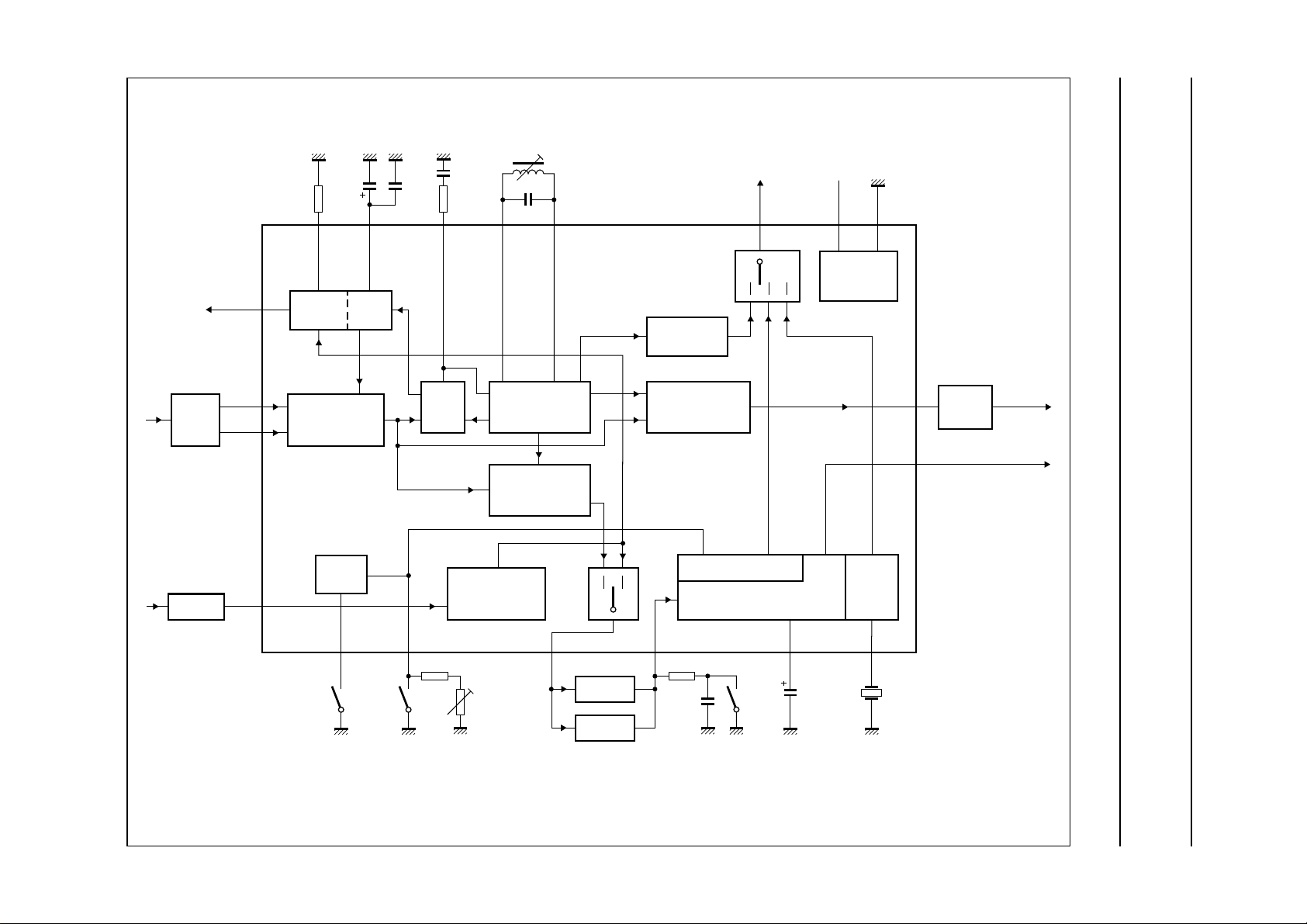
handbook, full pagewidth
BLOCK DIAGRAM
Single standard multimedia IF-PLL and FM
radio demodulator
Philips Semiconductors Preliminary specification
TV/radio
tuner AGC
VIF
SAW
10.7 MHz
TAGC
V
iVIF1
V
iVIF2
V
iRIF
TADJ
12
TUNER
AGC
1
VIF AMPLIFIER
2
AGC DETECTOR
4
AND
LOGIC
C
VAGC
VIF
AGC
T
PLL
FPLL
RIF AMPLIFIER
AGC DETECTOR
2 × f
PC
VCO
TWD
AND TV AFC
INTERCARRIER
MIXER
AND
AFC/RIF
level
14 1916156520 17
TV AFC
DETECTOR
VIDEO
DEMODULATOR
AND AMPLIFIER
TDA9809M
LEVEL DETECTOR
FM-PLL DEMODULATOR AND
AF SIGNAL PROCESSING
GNDV
P
INTERNAL
VOLTAGE
STABILIZER
RADIO
AFC
13
7
SOUND
TRAP
1.1 V (p-p)
video
1 V (p-p)
V
oAF
3
LP0
8
LP2
soft mute
threshold
adjust
V
o(int)
4.5 MHz
10.7 MHz
Fig.1 Block diagram.
9181110
V
iFM
forced
mute
C
DEC
10.7 MHz
ceramic
resonator
MHA957
TDA9809M
Philips Semiconductors Preliminary specification
Single standard multimedia IF-PLL and FM
radio demodulator
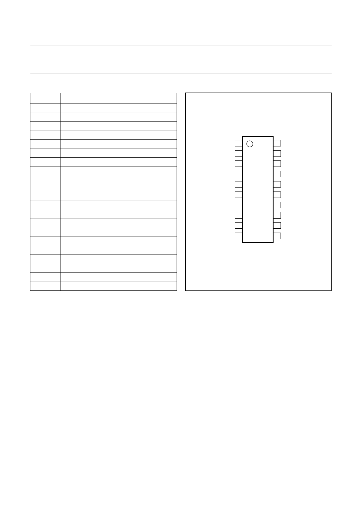
PINNING
SYMBOL PIN DESCRIPTION
V
iVIF1
V
iVIF2
LP0 3 logic port 0
V
iRIF
C
VAGC
T
PLL
V
oAF
LP2
C
DEC
V
o(int)
V
iFM
TAGC 12 TV/radio tuner AGC output
V
o(vid)
AFC 14 AFC/RIF level output
VCO1 15 VCO1 resonance circuit
VCO2 16 VCO2 resonance circuit
GND 17 ground
CERRES 18 ceramic resonator 10.7 MHz
V
P
TADJ 20 tuner AGC takeover point adjustment
1 VIF differential input signal voltage 1
2 VIF differential input signal voltage 2
4 RIF input
5 VIF AGC capacitor
6 PLL loop filter
7 audio output
logic port 2 and soft mute threshold
8
adjustment
9 decoupling capacitor
10 intercarrier output voltage
11 sound intercarrier input voltage
13 composite video output voltage
19 supply voltage
handbook, halfpage
V
1
iVIF1
V
2
iVIF2
LP0
3
V
4
iRIF
C
VAGC
T
PLL
V
oAF
LP2
C
DEC
V
o(int)
5
TDA9809M
6
7
8
9
10
MHA958
Fig.2 Pin configuration.
TDA9809M
TADJ
20
19
V
P
18
CERRES
17
GND
16
VCO2
VCO1
15
AFC
14
V
13
o(vid)
TAGC
12
V
11
iFM
FUNCTIONAL DESCRIPTION
The TDA9809M is comprised of the functional blocks
shown in Fig.1:
• Vision IF amplifier and AGC detector
• Tuner (TV/radio) and VIF AGC
• Frequency Phase-Locked Loop (FPLL) detector
• VCO, Travelling Wave Divider (TWD) and TV AFC
• Video demodulator and amplifier
• Intercarrier mixer
• RIF amplifier and AGC detector
• FM-PLL demodulator, level detector and radio AFC
• Audio Frequency (AF) signal processing
• Internal voltage stabilizer
• Logic.
1998 Jan 08 5
Vision IF amplifier and AGC detector
The vision IF amplifier contains three AC-coupled
differential amplifier stages. Each differential stage
includes a feedback network controlled by emitter
degeneration.
The AGC detector generates the required VIF gain control
voltage for constant video output by charging/discharging
the AGC capacitor. The sync level of the video signal is
therefore detected for negative video modulation.
Tuner (TV/radio) and VIF AGC
For TV operation, the AGC capacitor voltage is converted
to an internal IF control signal and then fed to the tuner
AGC to generate the tuner AGC output current at
pin TAGC (open-collector output). The tuner AGC
takeover point can be adjusted at pin TADJ. This allows
the tuner to be matched to the SAW filter in order to
achieve the optimum IF input level.
For FM radio operation, an AGC detector is provided to
obtain some adjacent channel protection.

Philips Semiconductors Preliminary specification
Single standard multimedia IF-PLL and FM
radio demodulator
Frequency Phased-Locked Loop detector (FPLL)
The VIF amplifier output signal is fed, via a limiting
amplifier, to a frequency and phase detector. During
acquisition, the frequency detector generates a DC current
that is proportional to the difference in frequency between
the input signal and the VCO signal.
After frequency lock-in, the phase detector generates a
DC current proportional to the phase difference between
the input signal and the VCO signal. The DC current
generated by the frequency or phase detector is converted
to a DC voltage via the loop filter, which controls the VCO
frequency.
VCO, TWD and TV AFC
The VCO operates with a resonance circuit (with L and C
in parallel) at double the Picture Carrier (PC) frequency.
The VCO is controlled by two integrated variable
capacitors. The control voltage required to tune the VCO
from its free-running frequency to double the PC frequency
is generated by the FPLL and fed via the loop filter to the
first variable capacitor. This control voltage is amplified
and converted into a current which represents the AFC
output signal. At the centre frequency, the AFC output
current is zero.
The TWD divides the oscillator signal by 2 and generates
two differential output signals with a 90° phase difference
independent of frequency.
TDA9809M
Intercarrier mixer
The intercarrier mixer is realized by a multiplier.
The sound IF signal passes through the vision IF SAW
filter and the composite IF signal is then fed to the
intercarrier mixer. Here, the IF signal is multiplied by the
90° TWD output signal to convert the sound IF to the
intercarrier frequency. By using this quadrature detection,
the low frequency video signals are removed. The mixer
output signal is fed, via a high-pass filter used to attenuate
the video signal components, at output pin 10.
RIF amplifier and AGC detector
The radio IF amplifier amplifies the 10.7 MHz radio IF
signal. This signal is supplied by the tuner and is fed to the
RIF input (pin 4) via a matching circuit and a ceramic
band-pass filter. This amplifier contains two stages.
The first stage, a conventional 0 dB differential amplifier
designed for optimal dynamic range, is followed by a
switchable differential amplifier stage with a gain of 10 dB.
Either the radio IF or the TV IF signal can be selected at
the output (pin 10).
The RIF output signal is fed via ceramic band-pass filters
to the FM-PLL demodulator and the radio IF AGC detector.
The AGC threshold is very high and is designed to obtain
some adjacent channel protection. The AGC detector
output is fed to the tuner AGC output stage (pin 12) to
control the tuner.
Video demodulator and amplifier
Video demodulation is realized by a multiplier designed for
low distortion and wide bandwidth. The vision IF input
signal and the ‘in-phase’ signal of the travelling wave
divider output are multiplied together.
The demodulated output signal is fed to the video amplifier
via an integrated low-pass filter used to attenuate the
carrier harmonics. This is an operational amplifier with
internal feedback and wide bandwidth. A low-pass filter is
integrated to attenuate the carrier harmonics. The video
output signal at V
modulation, in order to achieve 1 V (p-p) at the sound trap
output.
1998 Jan 08 6
is 1.1 V (p-p) for nominal vision IF
o(vid)
FM-PLL demodulator, level detector and radio AFC
The FM-PLL demodulator consists of a limiter and an FM
phase-locked loop. The 8-stage internally AC-coupled
limiter amplifies and limits the TV FM sound intercarrier or
the radio FM intermediate frequency signal prior to
demodulation. The limiter is designed for high sensitivity
and AM suppression with low DC offset and needs no
external pins for DC coupling.
Furthermore, the AF output signal can be force muted by
connecting a resistor between pin 11 and ground. The soft
mute function can be disabled by connecting a resistor
between pin 11 and the power supply. See the application
circuit in Fig.16.

Philips Semiconductors Preliminary specification
Single standard multimedia IF-PLL and FM
radio demodulator
The FM-PLL consists of an integrated relaxation oscillator,
an integrated loop filter and a phase detector.
The oscillator is locked to the FM intercarrier signal output
from the limiter. As a result of locking, the oscillator
frequency tracks with the modulation of the input signal
and the oscillator control voltage is superimposed on the
AF voltage. The FM-PLL operates as an FM demodulator.
The level detector detects, rectifies and amplifies the
output signals from the first 5 limiter stages. These signals
are then summed and the composite signal passed
through a low-pass filter, followed by a 6 dB output
amplifier. A DC voltage dependent on the limiter input level
is generated for controlling the behaviour of the AF soft
mute. The 6 dB output amplifier can be switched off via the
control logic and the level detector output signal fed to
pin 14. Furthermore, the steepness of the level detector
output signal tracks that of the power supply voltage.
The radio Automatic Frequency Control (AFC) stage is
comprised of a 10.7 MHz phase shifting network, a phase
detector (quadrature demodulator), a differential amplifier
input stage (which receives the limiting amplifier output
signal) and a current mode output stage.
A ceramic resonator is used for phase shifting. This
permits alignment-free operation.
AF signal processing
TDA9809M
Soft mute occurs when the internal level detector output
voltage is lower than the mute threshold voltage at pin 8
(provided an external resistor is not connected between
the limiter input, pin 11, and the supply voltage). The mute
stage reduces the AF signal by 25 dB, with an internal time
constant of approximately 7 ms.
If a resistor is connected between pin 11 and ground
(forced mute), the mute stage will reduce the AF signal by
more than 70 dB with the same time constant.
Otherwise, the AF signal will not be reduced.
The AF post-amplifier, which was designed to include a
rail-to-rail output stage, provides the required AF output
level at pin 7.
Internal voltage stabilizer
The bandgap circuit generates a voltage of approximately
1.25 V internally, independent of supply voltage and
temperature. A voltage regulator circuit connected to this
voltage generates a constant 3.6 V which is used as an
internal reference voltage.
Logic
The logic circuit detects the logic levels and threshold
voltages at ports LP0 and LP2 and controls the internal
functions as described in Table 2.
The AF signal processing stage consists of a pre-amplifier
for the FM-PLL demodulator output signal, an AF source
selector, a soft and forced mute stage with an integrated
time constant and an AF post-amplifier.
The FM demodulator output signal is pre-amplified by an
operational amplifier (30 dB gain) with internal feedback,
high gain and high common mode rejection. The feedback
circuit, together with external capacitor C
pin 9, keeps the DC level at the pre-amplifier output
constant (2.3 V). An external resistor connected in series
with C
The low-pass filter characteristic (130 kHz bandwidth) of
the amplifier reduces the harmonics of the IF signal at the
sound signal output.
provides a gain reduction capability.
DEC
connected to
DEC
1998 Jan 08 7
Philips Semiconductors Preliminary specification
Single standard multimedia IF-PLL and FM
TDA9809M
radio demodulator
LIMITING VALUES
In accordance with the Absolute Maximum Rating System (IEC 134).
SYMBOL PARAMETER CONDITIONS MIN. MAX. UNIT
V
P
V
n
t
sc
V
TAGC
T
stg
T
amb
V
es
Notes
1. I
= 102 mA; T
P
2. Machine model class B (L = 2.5 µH).
supply voltage (pin 19) maximum chip temperature of
− 5.5 V
130 °C; note 1
input voltage at pins 1 to 9, 11, 12, 14
0V
P
and 17 to 20
short-circuit time − 10 s
tuner AGC output voltage 0 13.2 V
storage temperature −25 +150 °C
ambient operating temperature −20 +70 °C
electrostatic handling note 2 −300 +300 V
=70°C; R
amb
th(j-a)
= 120 K/W.
V
THERMAL CHARACTERISTICS
SYMBOL PARAMETER CONDITIONS VALUE UNIT
R
th(j-a)
thermal resistance from junction to ambient in free air 120 K/W
CHARACTERISTICS
=5V; T
V
P
V
i(FM)(rms)
B/G: 10%; video signal in accordance with
=25°C; see Table 1 for input frequencies; input level V
amb
i(VIF)(rms)
= 10 mV (sync-level for B/G);
= 10 mV; IF input from 50 Ω via broadband transformer 1 : 1; video modulation DSB; residual carrier
“CCIR, line 17”
or
“NTC-7 Composite”
; test circuit in Fig.15 used for
measurements; unless otherwise specified.
SYMBOL PARAMETER CONDITIONS MIN. TYP. MAX. UNIT
Supply (pin 19)
V
P
I
P
supply voltage note 1 4.5 5 5.5 V
supply current TV mode 76 89 102 mA
radio mode 29 35 41 mA
power-down mode 5 8 11 mA
Television mode
V
ISION IF AMPLIFIER (PINS 1 AND 2)
V
i(VIF)(rms)
minimum vision IF
input signal voltage
fPC= 38.9 or 45.75 MHz;
−1 dB video at output
− 60 100 µV
(RMS value)
maximum vision IF
input signal voltage
= 38.9 or 45.75 MHz;
f
PC
+1 dB video at output
120 200 − mV
(RMS value)
1998 Jan 08 8

Philips Semiconductors Preliminary specification
Single standard multimedia IF-PLL and FM
TDA9809M
radio demodulator
SYMBOL PARAMETER CONDITIONS MIN. TYP. MAX. UNIT
∆V
o(int)
G
VIF(CR)
B
VIF(−3dB)
R
i(dif)
C
i(dif)
V
I
TRUE SYNCHRONOUS VIDEO DEMODULATOR; note 3
f
VCO(max)
/∆T oscillator drift as a
∆f
osc
V
VCO(rms)
f
cr(PC)
t
acq
V
i(VIF)(rms)
COMPOSITE VIDEO AMPLIFIER (PIN 13; SOUND CARRIER OFF)
V
o(video)(p-p)
V/S ratio of video
V
sync
V
clu
V
cll
R
o
internal IF amplitude
difference between
within AGC range;
∆f = 4.5 MHz
− 0.7 1 dB
picture and sound
carrier
VIF gain control range see Fig.3 65 70 − dB
−3 dB VIF bandwidth lower limit − 15 25 MHz
upper limit 70 100 − MHz
differential input
note 2 1.7 2.2 2.7 kΩ
resistance
differential input
note 2 1.2 1.7 2.5 pF
capacitance
DC input voltage note 2 − 3.4 − V
maximum oscillator
f=2f
PC
125 130 − MHz
frequency for carrier
regeneration
−6K−1
function of
oscillator is free-running;
I
= 0; note 4
AFC
−−±20 × 10
temperature
oscillator voltage
swing at
pins 15 and 16
fPC= 38.9 MHz 50 80 110 mV
f
= 45.75 MHz 40 65 90 mV
PC
(RMS value)
picture carrier capture
±1.4 ±1.8 − MHz
range
acquisition time Black Level (BL) = 70 kHz
−−30 ms
note 5
minimum vision IF
maximum IF gain; note 6 − 30 70 µV
input signal voltage for
PLL to be locked
(RMS value)
output signal voltage
see Fig.7 0.97 1.1 1.23 V
(peak-to-peak value)
1.9 2.33 3.0 −
(black-to-white) to
sync level
sync voltage level 1.4 1.5 1.6 V
upper video clipping
VP− 1.1 VP− 1 − V
voltage level
lower video clipping
− 0.7 0.9 V
voltage level
output resistance note 2 −−10 Ω
1998 Jan 08 9

Philips Semiconductors Preliminary specification
Single standard multimedia IF-PLL and FM
TDA9809M
radio demodulator
SYMBOL P ARAMETER CONDITIONS MIN. TYP. MAX. UNIT
I
bias(int)
I
o(sink)(max)
I
o(source)(max)
∆V
o(CVBS)
∆V
o(bl)(BG)
G
dif
ϕ
dif
B
v(−1dB)
B
v(−3dB)
S/N
W
S/N unweighted
α
IM(0.92/1.1)
α
IM(2.76/3.3)
α
r(vc)(rms)
α
H(sup)
α
H(spur)
PSRR power supply ripple
internal DC bias
current for
emitter-follower
maximum AC and DC
output sink current
maximum AC and DC
output source current
deviation of CVBS
output signal voltage
black level tilt in B/G
50 dB gain control −−0.5 dB
30 dB gain control −−0.1 dB
gain variation; note 7 −−1%
standard
differential gain
“CCIR, line 330”
or
“NTC-7 Composite”
differential phase
“CCIR, line 330”
or
“NTC-7 Composite”
−1 dB video bandwidth CL< 50 pF; RL>1kΩ;
AC load
−3 dB video bandwidth CL< 50 pF; RL>1kΩ;
AC load
weighted
see Fig.4 and note 8 54 58 − dB
signal-to-noise ratio
see Fig.4 and note 8 47 51 − dB
signal-to-noise ratio
intermodulation
attenuation at ‘blue’
intermodulation
attenuation at ‘yellow’
intermodulation
attenuation at ‘blue’
intermodulation
attenuation at ‘yellow’
residual vision carrier
(RMS value)
harmonics
fIM= 0.92 or 1.1 MHz;
see Fig.5 and note 9
= 0.92 or 1.1 MHz;
f
IM
see Fig.5 and note 9
fIM= 2.76 or 3.3 MHz;
see Fig.5 and note 9
f
= 2.76 or 3.3 MHz;
IM
see Fig.5 and note 9
fundamental wave and
harmonics
note 10a 35 40 − dB
suppression in video
signal
spurious element
note 10b 40 −− dB
suppression
video signal; grey level; see
rejection at pin 13
Fig.9
2.2 3.0 − mA
1.6 −− mA
2.9 −− mA
− 25 %
− 2 4 deg
56− MHz
78− MHz
52 58 − dB
54 60 − dB
52 58 − dB
54 60 − dB
− 25 mV
30 35 − dB
1998 Jan 08 10
Philips Semiconductors Preliminary specification
Single standard multimedia IF-PLL and FM
TDA9809M
radio demodulator
SYMBOL PARAMETER CONDITIONS MIN. TYP. MAX. UNIT
VIF-AGC DETECTOR (PIN 5)
I
ch
I
dch
t
res(AGC)(r)
t
res(AGC)(f)
TV TUNER AGC (PIN 12)
V
i(rms)
V
o(max)
V
sat
∆V
/∆T variation of takeover
TOP
I
sink
∆G
IF
TV AFC DETECTOR (PIN 14); see Fig.6 and note 12
CR
stps
∆f
/∆T frequency variation
IF
V
o(max)
V
o(min)
I
o(source)
I
o(sink)
∆I
r(mod)(p-p)
charge current note 7 0.75 1 1.25 mA
discharge current 15 20 25 µA
AGC response time to
note 11 − 0.05 0.1 ms/dB
a rising VIF step
AGC response time to
− 2.2 3.5 ms/dB
a falling VIF step
IF input signal voltage
for minimum onset of
input at pins 1 and 2;
R
=22kΩ; I12= 0.4 mA
TOP
− 25 mV
tuner takeover
(RMS value)
IF input signal voltage
for maximum onset of
input at pins 1 and 2;
R
=0Ω; I12= 0.4 mA
TOP
50 100 − mV
tuner takeover
(RMS value)
tuner takeover point
=13kΩ; I12= 0.4 mA 5 − 20 mV
R
TOP
accuracy (RMS value)
maximum output
voltage
from external source;
note 2
−−13.2 V
saturation voltage I12= 1.5 mA −−0.2 V
I12= 0.4 mA − 0.03 0.07 dB/K
point with temperature
sink current see Fig.3
no tuner gain reduction;
V
= 13.2 V
12
maximum tuner gain
−−1 µA
1.5 2 2.6 mA
reduction
IF slip by automatic
gain control
control steepness
∆I14/∆f
tuner gain current from
− 68 dB
20 to 80%
fPC= 38.9 MHz; note 13 0.5 0.75 1.0 µA/kHz
= 45.75 MHz; note 13 0.4 0.65 0.9 µA/kHz
f
PC
I
= 0; note 4 −−±20 × 10
AFC
−6K−1
with temperature
output voltage upper
limit
output voltage lower
see Fig.6 without external
components
VP− 0.6 VP− 0.3 − V
− 0.3 0.6 V
limit
output source current 150 200 250 µA
output sink current 150 200 250 µA
residual video
− 20 30 µA
modulation current
(peak-to-peak value)
1998 Jan 08 11

Philips Semiconductors Preliminary specification
Single standard multimedia IF-PLL and FM
TDA9809M
radio demodulator
SYMBOL PARAMETER CONDITIONS MIN. TYP. MAX. UNIT
INTERCARRIER MIXER (PIN 10)
V
o(intercarrier)(rms)
IF intercarrier level
(RMS value)
B
−3dB
−3 dB intercarrier
bandwidth
α
r(SC)(rms)
residual sound carrier
(RMS value)
α
r(VC)(rms)
residual vision carrier
(RMS value)
α
H(sup)
suppression of video
signal harmonics
R
o
V
O
I
bias(int)
output resistance note 2 − 25 −Ω
DC output voltage − 2.0 − V
DC internal bias
current for
emitter-follower
I
o(sink)(max)
maximum AC and DC
output sink current
I
o(source)(max)
maximum AC and DC
output source current
LIMITER AMPLIFIER (PIN 11); note 15
V
i(FM)(rms)
input signal voltage for
lock-in (RMS value)
input signal voltage
(RMS value)
allowed input signal
voltage (RMS value)
α
AM
R
i
V
I
AM suppression 50 µs de-emphasis;
input resistance note 2 480 600 720 Ω
DC input voltage − 2.65 − V
FM-PLL DEMODULATOR
f
cr(PLL)
f
hr(PLL)
t
acq
catching range of PLL upper limit 7.0 −− MHz
holding range of PLL upper limit 9.0 −− MHz
acquisition time −−4 µs
sound carrier 1 (SC1);
− 32 − mV
SC2off; note 14
upper limit 7.5 9 − MHz
fundamental wave and
− 25 mV
harmonics
fundamental wave and
− 25 mV
harmonics
intercarrier mode;
f
≤ 5 MHz
video
39 −− dB
2.7 3.4 − mA
1.5 2.0 − mA
2.5 −− mA
−−100 µV
SN+
-------------N
weighted 40 dB=
− 250 500 µV
200 −− mV
46 50 − dB
AM: f
= 1 kHz; m = 0.3
mod
referenced to 27 kHz
(54% FM deviation)
lower limit −−4.0 MHz
lower limit −−3.5 MHz
1998 Jan 08 12
 Loading...