

Page 1

TDA8944J
2 x 7 W stereo Bridge Tied Load (BTL) audio amplifier
Rev. 02 — 14 February 2000 Product specification
1. General description
The TDA8944J is a dual-channel audio power amplifier with an output power of
2 × 7 W at an 8 Ω load and a 12 V supply. The circuit contains two Bridge Tied Load
(BTL) amplifierswith an all-NPN output stage and standby/mutelogic. The TDA8944J
comes in a 17-pin DIL-bent-SIL (DBS) power package. The TDA8944J is
printed-circuit board (PCB) compatible with all other types in the TDA894x family.
One PCB footprint accommodates both the mono and the stereo products.
2. Features
■ Few external components
■ Fixed gain
■ Standby and mute mode
■ No on/off switching plops
■ Low standby current
■ High supply voltage ripple rejection
■ Outputs short-circuit protected to ground, supply and across the load
c
c
■ Thermally protected
■ Printed-circuit board compatible.
3. Applications
■ Mains fed applications (e.g. TV sound)
■ PC audio
■ Portable audio.
4. Quick reference data
Table 1: Quick reference data
Symbol Parameter Conditions Min Typ Max Unit
V
CC
I
q
I
stb
supply voltage 6 12 18 V
quiescent supply current VCC=12V; RL= ∞ - 2436mA
standby supply current - - 10 µA
Page 2
Philips Semiconductors
TDA8944J
2 x 7 W stereo BTL audio amplifier
Table 1: Quick reference data
Symbol Parameter Conditions Min Typ Max Unit
P
o
THD total harmonic distortion P
G
v
SVRR supply voltage ripple
5. Ordering information
Table 2: Ordering information
Type number Package
TDA8944J DBS17P plastic DIL-bent-SIL power package;
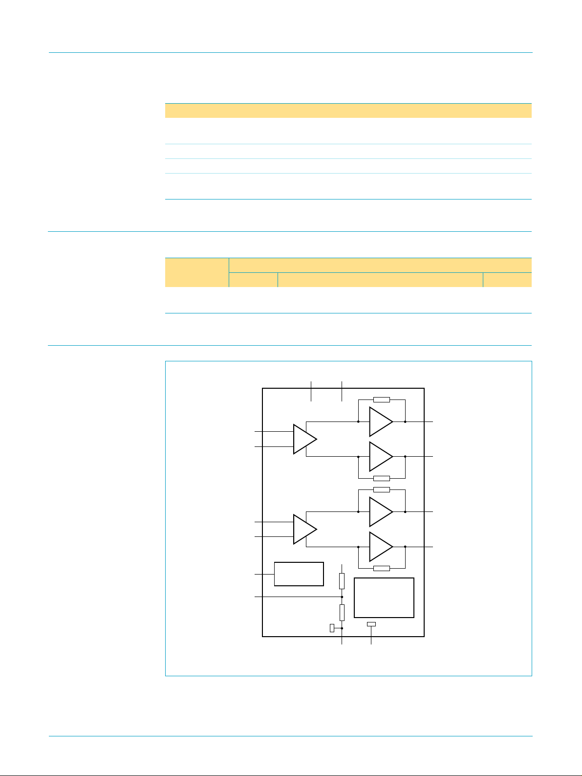
6. Block diagram
dth
…continued
output power THD = 10%; RL=8Ω;
=12V
V
CC
= 1 W - 0.03 0.1 %
o
67- W
voltage gain 31 32 33 dB
50 65 - dB
rejection
Name Description Version
SOT243-1
17 leads (lead length 12 mm)
CC1
V
CC2
V
IN1−
IN1+
IN2−
IN2+
MODE
SVR
Fig 1. Block diagram.
8
6
9
12
10
STANDBY/
MUTE LOGIC
11
3
TDA8944J
16
V
CC
20
kΩ
SHORT CIRCUIT
TEMPERATURE
20
kΩ
GND115GND2
PROTECTION
2
AND
14
17
MBK933
1
OUT1−
4
OUT1+
OUT2−
OUT2+
9397 750 06861
© Philips Electronics N.V. 2000. All rights reserved.
Product specification Rev. 02 — 14 February 2000 2 of 21
Page 3

Philips Semiconductors
7. Pinning information
7.1 Pinning
TDA8944J
2 x 7 W stereo BTL audio amplifier
handbook, halfpage
OUT1−
GND1
V
CC1
OUT1+
n.c.
IN1+
n.c.
IN1−
IN2−
MODE
SVR
IN2+
n.c.
OUT2−
GND2
V
CC2
OUT2+
1
2
3
4
5
6
7
8
9
TDA8944J
10
11
12
13
14
15
16
17
MBK936
Fig 2. Pin configuration.
7.2 Pin description
Table 3: Pin description
Symbol Pin Description
OUT1− 1 negative loudspeaker terminal 1
GND1 2 ground channel 1
V
CC1
OUT1+ 4 positive loudspeaker terminal 1
n.c. 5 not connected
IN1+ 6 positive input 1
n.c. 7 not connected
IN1− 8 negative input 1
IN2− 9 negative input 2
MODE 10 mode selection input (standby, mute, operating)
SVR 11 half supply voltage decoupling (ripple rejection)
IN2+ 12 positive input 2
9397 750 06861
Product specification Rev. 02 — 14 February 2000 3 of 21
3 supply voltage channel 1
© Philips Electronics N.V. 2000. All rights reserved.
Page 4

Philips Semiconductors
TDA8944J
2 x 7 W stereo BTL audio amplifier
Table 3: Pin description
Symbol Pin Description
n.c. 13 not connected
OUT2− 14 negative loudspeaker terminal 2
GND2 15 ground channel 2
V
CC2
OUT2+ 17 positive loudspeaker terminal 2
8. Functional description
The TDA8944J is a stereo BTL audio power amplifier capable of delivering 2 × 7W
output power to an 8 Ω load at THD = 10%, using a 12 V power supply and an
external heatsink. The voltage gain is fixed at 32 dB.
With the three-level MODE input the device can be switched from ‘standby’ to ‘mute’
and to ‘operating’ mode.
The TDA8944J outputs are protected by an internal thermal shutdown protection
mechanism and a short-circuit protection.
8.1 Input configuration
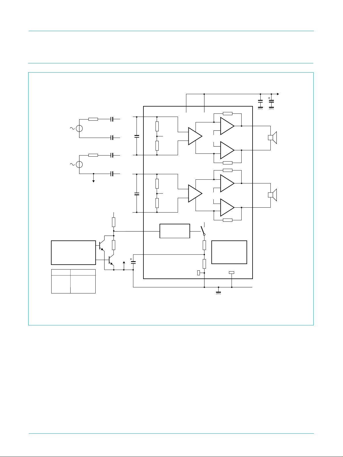
The TDA8944J inputs can be driven symmetrical (floating) as well as asymmetrical.
In the asymmetrical mode one input pin is connected via a capacitor to the signal
ground which should be as close as possible to the SVR (electrolytic) capacitor
ground. Note that the DC level of the input pins is half of the supply voltage VCC, so
coupling capacitors for both pins are necessary.
…continued
16 supply voltage channel 2
The input cut-off frequency is:
f
icut off–()
=
1
------------------------------ -
2RiCi×()–
(1)
For Ri=45kΩ and Ci= 220 nF:
f
i cut off–()
------------------------------------------------------------------ -
24510
1
3
× 220× 109–×()–
16 Hz==
(2)
As shown in Equation 1 and 2, large capacitor values for the inputs are not
necessary; so the switch-on delay during charging of the input capacitors, can be
minimized. This results in a good low frequency response and good switch-on
behaviour.
Remark: TopreventHF oscillations do not leave the inputs open, connect a capacitor
of at least 1.5 nF across the input pins close to the device.
9397 750 06861
Product specification Rev. 02 — 14 February 2000 4 of 21
© Philips Electronics N.V. 2000. All rights reserved.
Page 5

Philips Semiconductors
8.2 Power amplifier
The power amplifier is a Bridge Tied Load (BTL) amplifier with an all-NPN output
stage, capable of delivering a peak output current of 2 A.
The BTL principle offers the following advantages:
•
•
•
•
8.2.1 Output power measurement
The output power as a function of the supply voltage is measured on the output pins
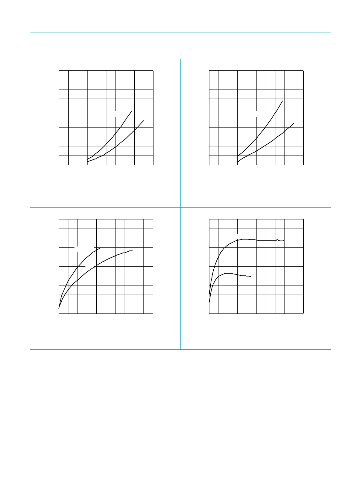
at THD = 10%; see Figure 8. The maximum output power is limited by the maximum
supply voltage of 12 V and the maximum available output current: 2 A repetitive peak
current.
8.2.2 Headroom
Typical CD music requires at least 12 dB (factor 15.85) dynamic headroom –
compared to the average power output – for transferring the loudest parts without
distortion. At VCC=12V, RL=8Ω and Po= 4 W at THD = 0.1% (see Figure 6), the
Average Listening Level (ALL) – music power – without any distortion yields:
P
TDA8944J
2 x 7 W stereo BTL audio amplifier
Lower peak value of the supply current
The ripple frequency on the supply voltage is twice the signal frequency
No expensive DC-blocking capacitor
Good low frequency performance.
= 4 W/15.85 = 252 mW.
o(ALL)
The power dissipation can be derived from Figure 11 on page 10 for 0 dB
respectively 12 dB headroom.
Table 4: Power rating as function of headroom
Headroom Power output (THD = 0.1%) Power dissipation (P)
0 dB P
12 dB P
=4W 8W
o
= 252 mW 4 W
o(ALL)
For the average listening level a power dissipation of 4 W can be used for a heatsink
calculation.
8.3 Mode selection
The TDA8944J has three functional modes, which can be selected by applying the
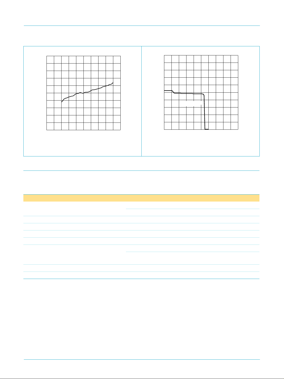
proper DC voltage to pin MODE. See Figure 4 and 5 for the respective DC levels,
which depend on the supply voltage level. The MODE pin can be driven by a 3-state
logic output stage: e.g. a microcontroller with additional components for DC-level
shifting.
Standby — In this mode the current consumption is very low and the outputs are
floating. The device is in standby mode when (VCC− 0.5 V) < V
the MODE pin is left floating (high impedance). The power consumption of the
TDA8944J will be reduced to <0.18 mW.
MODE<VCC
, or when
9397 750 06861
Product specification Rev. 02 — 14 February 2000 5 of 21
© Philips Electronics N.V. 2000. All rights reserved.
Page 6

Philips Semiconductors
Mute — In this mode the amplifier is DC-biased but not operational (no audio output);
the DC level of the input and output pins remain on half the supply voltage. This
allows the input coupling and Supply Voltage Ripple Rejection (SVRR) capacitors to
be charged to avoid pop-noise. The device is in mute mode when
3V<V
Operating — In this mode the amplifier is operating normally. The operating mode is
activated at V
8.3.1 Switch-on and switch-off
To avoid audible plops during supply voltage switch-on or switch-off, the device is set
to standby mode before the supply voltage is applied (switch-on) or removed
(switch-off).
The switch-on and switch-off time can be influenced by an RC-circuit on the MODE
pin. Rapid on/off switching of the device or the MODE pin may cause ‘click- and
pop-noise’. This can be prevented by proper timing of the RC-circuit on the MODE
pin.
<(VCC− 1.5 V).
MODE
MODE
TDA8944J
2 x 7 W stereo BTL audio amplifier
< 0.5 V.
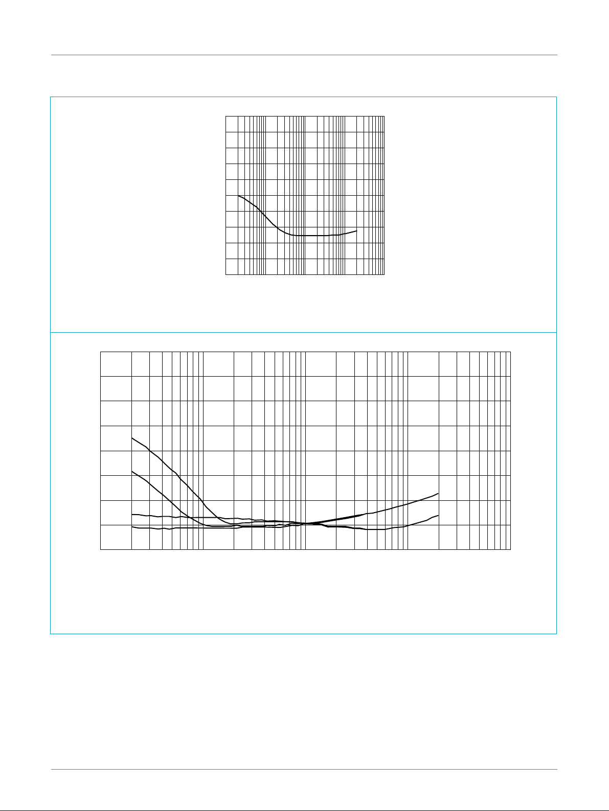
8.4 Supply Voltage Ripple Rejection (SVRR)
The SVRR is measured with an electrolytic capacitor of 10 µF on pin SVR at a
bandwidth of 10 Hz to 80 kHz. Figure 13 on page 11 illustrates the SVRR as function
of the frequency. A larger capacitor value on the SVR pin improves the ripple rejection
behaviour at the lower frequencies.
8.5 Built-in protection circuits
The TDA8944J contains two types of protection circuits, i.e. short-circuit and thermal
shutdown.
8.5.1 Short-circuit protection
Short-circuit to ground or supply line — This is detected by a so-called ‘missing
current’ detection circuit which measures the current in the positive supply line and
the current in the ground line. A difference between both currents larger than 0.4 A,
switches the power stage to standby mode (high impedance).
Short-circuit across the load — This is detected by an absolute-current
measurement. An absolute-current larger than 2 A, switches the power stage to
standby mode (high impedance).
8.5.2 Thermal shutdown protection
The junction temperature is measured by a temperature sensor; at a junction
temperature of approximately 150 °C this detection circuit switches the power stage
to standby mode (high impedance).
9397 750 06861
Product specification Rev. 02 — 14 February 2000 6 of 21
© Philips Electronics N.V. 2000. All rights reserved.
Page 7

Philips Semiconductors
TDA8944J
2 x 7 W stereo BTL audio amplifier
9. Limiting values
Table 5: Limiting values
In accordance with the Absolute Maximum Rating System (IEC 60134).
Symbol Parameter Conditions Min Max Unit
V
CC
supply voltage no signal −0.3 +25 V
operating −0.3 +18 V
V
I
I
ORM
T
stg
T
amb
P
tot
V
CC(sc)
input voltage −0.3 VCC+ 0.3 V
repetitive peak output current - 2 A
storage temperature non-operating −55 +150 °C
operating ambient temperature −40 +85 °C
total power dissipation - 18 W
supplyvoltagetoguaranteeshort-circuit
-15V
protection
10. Thermal characteristics
Table 6: Thermal characteristics
Symbol Parameter Conditions Value Unit
R
th(j-a)
R
th(j-mb)
thermal resistance from junction to ambient in free air 40 K/W
thermal resistance from junction to mounting base both channels driven 6.9 K/W
11. Static characteristics
Table 7: Static characteristics
VCC=12V; T
Symbol Parameter Conditions Min Typ Max Unit
V
CC
I
q
I
stb
V
O
[3]
∆V
OUT
V
MODE
I
MODE
[1] With a load connected at the outputs the quiescent current will increase, the maximum of this increase being equal to the differential
output voltage offset (∆V
[2] The DC output voltage with respect to ground is approximately 0.5VCC.
[3] ∆V
OUT
=25°C; RL=8Ω; V
amb
supply voltage operating 6 12 18 V
quiescent supply current RL= ∞
standby supply current V
DC output voltage
differential output voltage offset - - 200 mV
mode selection input voltage operating mode 0 - 0.5 V
mode selection input current 0 < V
= V
OUT+
− V
=0V; Vi= 0 V; measured in test circuit Figure 14; unless otherwise specified.
MODE
) divided by the load resistance (RL).
OUT
OUT−
[1]
- 2436mA
MODE=VCC
--10µA
[2]
-6-V
mute mode 3 - V
standby mode V
MODE<VCC
− 0.5 - V
CC
--20µA
− 1.5 V
CC
CC
V
9397 750 06861
Product specification Rev. 02 — 14 February 2000 7 of 21
© Philips Electronics N.V. 2000. All rights reserved.
Page 8
Philips Semiconductors
TDA8944J
2 x 7 W stereo BTL audio amplifier
V
MODE
MGL955
20
(V)
50
handbook, halfpage
I
q
(mA)
40
30
20
10
0
0481216
MGL954
VCC (V)
20
Fig 3. Quiescent current as function of supply
50
handbook, halfpage
I
q
(mA)
40
30
20
10
0
0481216
VCC = 12 V
Fig 4. Quiescent current as function of mode voltage.
voltage.
12. Dynamic characteristics
Table 8: Dynamic characteristics
VCC=12V; T
22 Hz to 22 kHz; unless otherwise specified.
Symbol Parameter Conditions Min Typ Max Unit
P
o
THD total harmonic distortion P
G
v
Z
i(dif)
V
n(o)
SVRR supply voltage ripple rejection f
V
o(mute)
α
cs
=25°C; RL=8Ω; f = 1 kHz; V
amb
= 0 V; measured in test circuit Figure 14; audio pass band
MODE
output power THD = 10% 6 7 - W
THD = 0.5% 4 5 - W
= 1 W - 0.03 0.1 %
o
voltage gain 31 32 33 dB
differential input impedance 70 90 110 kΩ
noise output voltage
ripple
f
ripple
= 1 kHz
= 100 Hz
[1]
- 90 120 µV
[2]
50 65 - dB
[2]
-60-dB
to 20 kHz
output voltage mute mode
[3]
--50µV
channel separation Rs=0Ω 50 75 - dB
[1] The noise output voltage is measured at the output in a frequency range from 20 Hz to 20 kHz (unweighted), with a source impedance
Rs=0Ω at the input.
[2] Supply voltage ripple rejection is measured at the output, with a source impedance Rs=0Ω at the input. The ripple voltage is a sine
wave with a frequency f
and an amplitude of 707 mV (RMS), which is applied to the positive supply rail.
ripple
[3] Output voltage in mute mode is measured with an input voltage of 1 V (RMS) in a bandwidth of 20 kHz, so including noise.
9397 750 06861
© Philips Electronics N.V. 2000. All rights reserved.
Product specification Rev. 02 — 14 February 2000 8 of 21
Page 9
Philips Semiconductors
TDA8944J
2 x 7 W stereo BTL audio amplifier
10
handbook, full pagewidth
V
o
(V)
1
−1
10
−2
10
−3
10
−4
10
−5
10
840
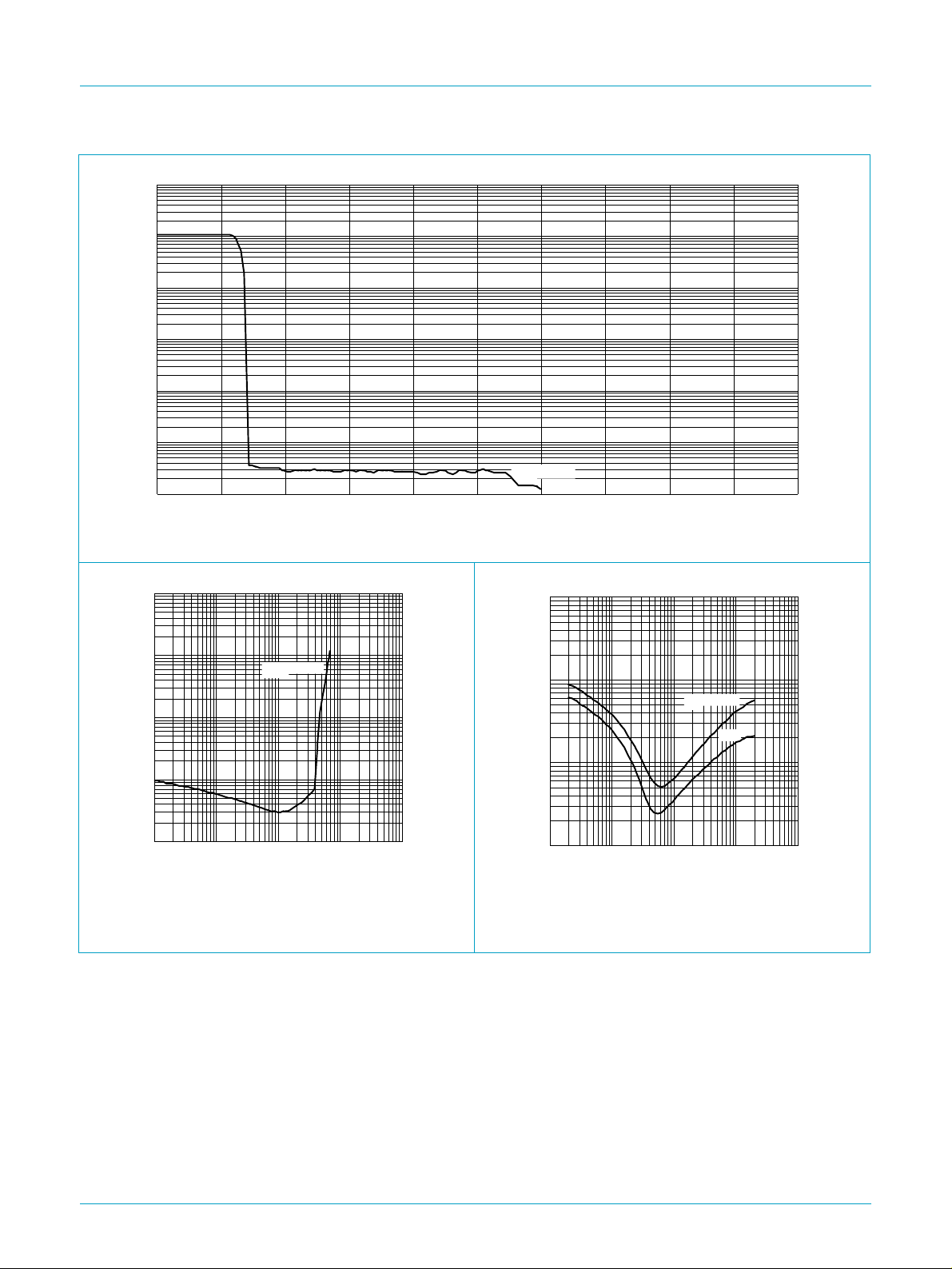
Fig 5. Output voltage as function of mode voltage.
2
10
handbook, halfpage
THD
(%)
10
1
−1
10
VCC = 12 V
MGL952
VCC = 12 V
12
10
handbook, halfpage
THD
(%)
1
−1
10
V
MODE
Po = 0.1 W
1 W
(V)
MGL957
2016
MGL953
−2
10
−2
10
−1
10110
Po (W)
2
10
−2
10
10 10
2
10
3
10
4
10
5
f (Hz)
No bandpass filter applied.
Fig 6. Total harmonic distortion as function of output
power.
9397 750 06861
Fig 7. Total harmonic distortion as function of
frequency.
© Philips Electronics N.V. 2000. All rights reserved.
Product specification Rev. 02 — 14 February 2000 9 of 21
Page 10
Philips Semiconductors
TDA8944J
2 x 7 W stereo BTL audio amplifier
20
handbook, halfpage
P
o
(W)
16
12
8
4
0
0481216
RL = 8 Ω
16 Ω
MGL959
VCC (V)
20
handbook, halfpage
P
tot
(W)
16
12
8
4
20
0
0481216
RL = 8 Ω
16 Ω
MGL960
VCC (V)
20
THD = 10%.
Fig 8. Output power as function of supply voltage. Fig 9. Total power dissipation as function of supply
voltage.
100
handbook, halfpage
η
(%)
80
MGL962
10
handbook, halfpage
P
(W)
8
RL = 8 Ω
MGL961
RL = 16 Ω
60
8 Ω
40
20
0
02468
Po (W)
10
6
4
2
0
02468
16 Ω
Po (W)
10
VCC=12V.
Fig 10. Efficiency as function of output power. Fig 11. Power dissipation as function of output power.
9397 750 06861
© Philips Electronics N.V. 2000. All rights reserved.
Product specification Rev. 02 — 14 February 2000 10 of 21
Page 11
Philips Semiconductors
TDA8944J
2 x 7 W stereo BTL audio amplifier
handbook, halfpage
0
α
cs
(dB)
−20
−40
−60
−80
−100
10 10
2
No bandpass filter applied.
Fig 12. Channel separation as function of frequency.
handbook, full pagewidth
0
SVRR
(dB)
−20
MGL958
3
10
4
10
f (Hz)
5
10
MGL956
−40
−60
−80
VCC= 12 V; Rs=0Ω; V
B
A
2
10
ripple
10
= 707 mV (peak-to-peak); no bandpass filter applied.
3
10
Curves A: inputs short-circuited
Curves B: inputs short-circuited and connected to ground (asymmetrical application)
Fig 13. Supply voltage ripple rejection as function of frequency.
CH2
CH1
4
10
f (Hz)
5
10
9397 750 06861
© Philips Electronics N.V. 2000. All rights reserved.
Product specification Rev. 02 — 14 February 2000 11 of 21
Page 12
Philips Semiconductors
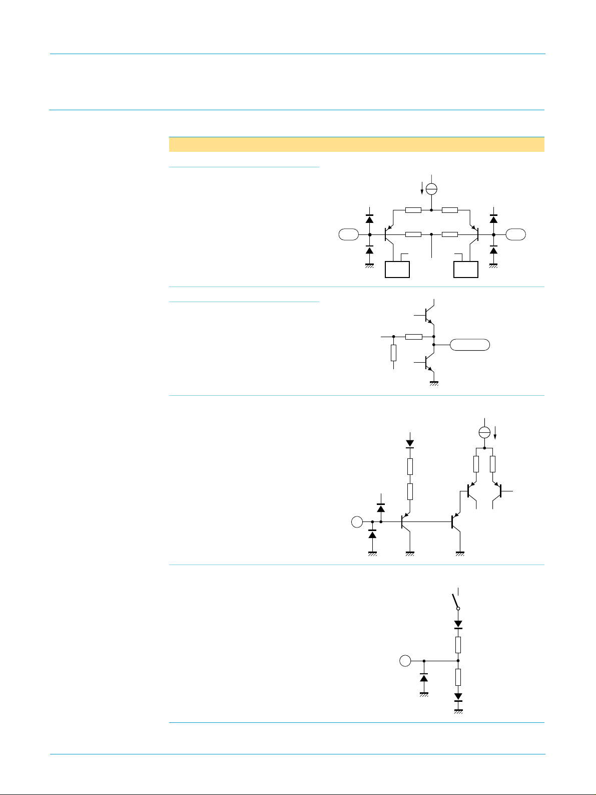
13. Internal circuitry
Table 9: Internal circuitry
Pin Symbol Equivalent circuit
6 and 8 IN1+ and IN1−
12 and 9 IN2+ and IN2−
TDA8944J
2 x 7 W stereo BTL audio amplifier
V
CC
1 and 4 OUT1− and OUT1+
14 and 17 OUT2− and OUT2+
10 MODE
1 kΩ
V
CC
MGL946
V
CC
1 kΩ
V
CC
8, 9 6, 12
V
1.5 kΩ 1.5 kΩ
45 kΩ 45 kΩ
1/2 V
1 : 1 1 : 1
40 Ω
1/2 V
CC
CC
100 Ω
V
CC
(SVR)
10 kΩ
10 kΩ
CC
1, 4, 14, 17
MGL947
10
OFF
HIGH
MUTE
HIGH
MGL949
11 SVR
V
CC
Standby
20 kΩ
11
20 kΩ
MGL948
9397 750 06861
Product specification Rev. 02 — 14 February 2000 12 of 21
© Philips Electronics N.V. 2000. All rights reserved.
Page 13
Philips Semiconductors
14. Application information
220 nF
R
s
Symmetrical
input
R
Asymmetrical
input
signal
GND
C
i
1.5
220 nF
220 nF
s
C
i
220 nF
1.5
V
CC
R
IN1−
nF
IN1+
IN2−
nF
IN2+
MODE
TDA8944J
2 x 7 W stereo BTL audio amplifier
+V
CC
100 nF
8
R
i
45 kΩ
1/2 V
R
i
45 kΩ
6
3
CC
16
−
1/2 V
+
CC
+
−
−
+
−
+
1
4
OUT1−
OUT1+
TDA8944J
9
1/2 V
−
+
CC
+
−
R
i
45 kΩ
1/2 V
R
i
45 kΩ
12
10
STANDBY/
MUTE LOGIC
CC
−
+
−
+
V
CC
14
17
OUT2−
OUT2+
1000 µF
R
L
8 Ω
R
L
8 Ω
C1
MICROCONTROLLER
C2
On
C1 C2
0
0
1
0
1
0
MODE
Standby
Mute
Fig 14. Application diagram.
14.1 Printed-circuit board (PCB)
14.1.1 Layout and grounding
R
signal
GND
SVR
10
µF
20 kΩ
1/2 V
11
ull pagewidth
CC
20 kΩ
SHORT CIRCUIT
AND
TEMPERATURE
PROTECTION
152
GND
MGL950
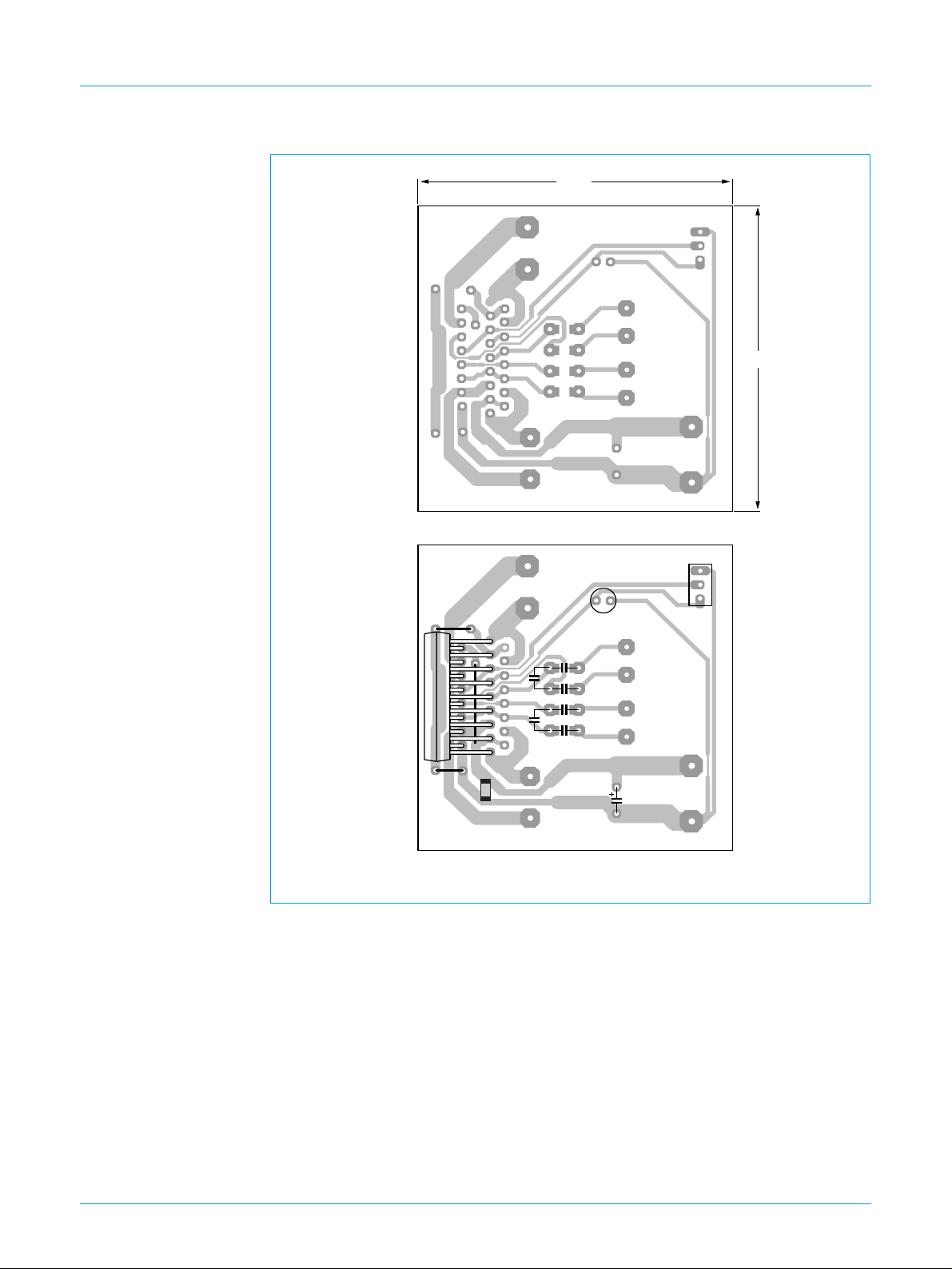
For a high system performance level certain grounding techniques are essential.
The input referencegrounds haveto be tied with their respective source grounds and
must have separate tracks from the power ground tracks; this will prevent the large
(output) signal currents from interfering with the small AC input signals.
The small-signal ground tracks should be physically located as far as possible from
the power ground tracks. Supply and output tracks should be as wide as possible for
delivering maximum output power.
9397 750 06861
© Philips Electronics N.V. 2000. All rights reserved.
Product specification Rev. 02 — 14 February 2000 13 of 21
Page 14
Philips Semiconductors
TDA8944J
2 x 7 W stereo BTL audio amplifier
1.5 nF
54 mm
OUT2−
OUT2+
220 nF
+−
10 µF
56 mm
ON
MUTE
IN2−
IN2+
IN1−
dth
17
220 nF
1
OUT1−
100 nF
OUT1+
IN1+
1000 µF
V
CC
GND
MGL951
Fig 15. Printed-circuit board layout (single-sided); components view.
14.1.2 Power supply decoupling
Proper supply bypassing is critical for low-noise performance and high supply voltage
ripple rejection. The respective capacitor locations should be as close as possible to
the device and grounded to the power ground. Proper power supply decoupling also
prevents oscillations.
For suppressing higher frequency transients (spikes) on the supply line a capacitor
with low ESR – typical 100 nF – has to be placed as close as possible to the device.
For suppressing lower frequency noise and ripple signals, a large electrolytic
capacitor – e.g. 1000 µF or greater – must be placed close to the device.
The bypass capacitor on the SVR pin reduces the noise and ripple on the midrail
voltage. For good THD and noise performance a low ESR capacitor is recommended.
9397 750 06861
Product specification Rev. 02 — 14 February 2000 14 of 21
© Philips Electronics N.V. 2000. All rights reserved.
Page 15

Philips Semiconductors
14.2 Thermal behaviour and heatsink calculation
TDA8944J
2 x 7 W stereo BTL audio amplifier
The measured maximum thermal resistance of the IC package, R
th(j-mb)
is 6.9 K/W.
A calculation for the heatsink can be made, with the following parameters:
T
amb(max)
=50°C
VCC= 12 V and RL=8Ω
T
= 150 °C.
j(max)
R
is the total thermal resistance between the junction and the ambient
th(tot)
including the heatsink. In the heatsink calculations the value of R
th(mb-h)
is ignored.
At VCC= 12 V and RL=8Ω the measured worstcase sine-wave dissipation is 8 W;
see Figure 11. For T
= 150 °C the temperature raise - caused by the power
j(max)
dissipation - is: 150 – 50 = 100 °C.
P × R
R
th(tot)
R
th(h-a)=Rth(tot)–Rth(j-mb)
= 100 °C
th(tot)
= 100/8 = 12.5 K/W
= 12.5 – 6.9 = 5.6 K/W.
The calculation above is for an application at worstcase (stereo) sine-wave output
signals. In practice music signals will be applied, which decreases the maximum
power dissipation to approximately half of the sine-wave power dissipation (see
Section 8.2.2). This allows for the use of a smaller heatsink:
P × R
R
th(tot)
R
th(h-a)=Rth(tot)–Rth(j-mb)
= 100 °C
th(tot)
= 100/4 = 25 K/W
= 25 – 6.9 = 18.1 K/W.
To increase the lifetime of the IC, T
heatsink of approximately 12 K/W for music signals.
15. Test information
15.1 Quality information
The
applicable.
15.2 Test conditions
T
amb
unless otherwise specified.
Remark: In the graphs as function of frequency no bandpass filter was applied; see
Figure 7, 12 and 13.
should be reduced to 125 °C. This requires a
j(max)
General Quality Specification for Integrated Circuits, SNW-FQ-611D
is
=25°C; VCC= 12 V; f = 1 kHz; RL=8Ω; audio pass band 22 Hz to 22 kHz;
9397 750 06861
Product specification Rev. 02 — 14 February 2000 15 of 21
© Philips Electronics N.V. 2000. All rights reserved.
Page 16
Philips Semiconductors
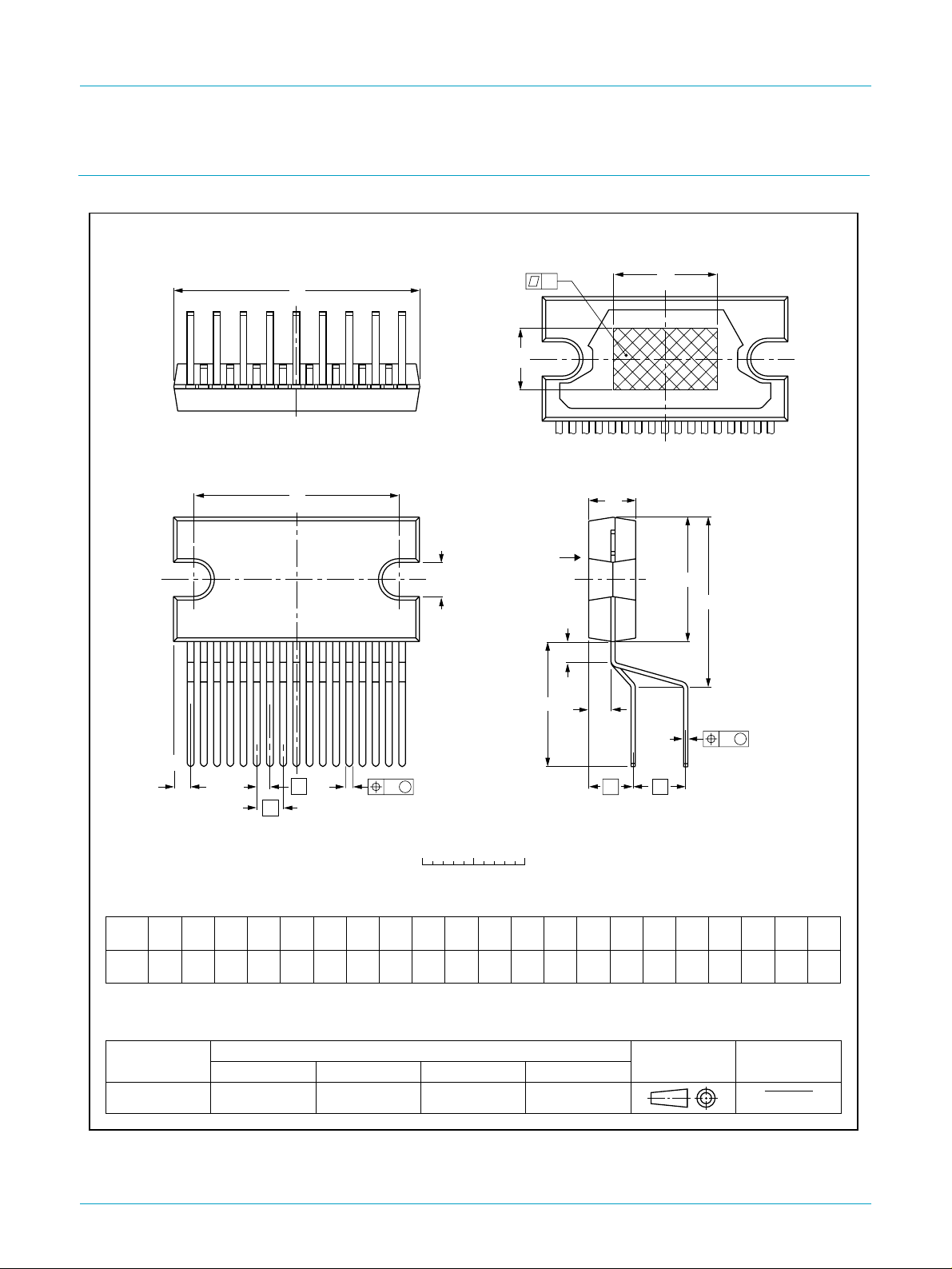
16. Package outline
TDA8944J
2 x 7 W stereo BTL audio amplifier
DBS17P: plastic DIL-bent-SIL power package; 17 leads (lead length 12 mm)
non-concave
D
d
j
x
E
h
view B: mounting base side
B
L
3
SOT243-1
D
h
A
2
E
A
117
e
0.48
0.38
1
e
(1)
deD
24.0
20.0
23.6
19.6
Z
DIMENSIONS (mm are the original dimensions)
UNIT A e
mm
Note
1. Plastic or metal protrusions of 0.25 mm maximum per side are not included.
OUTLINE
VERSION
SOT243-1
A2bpcD
17.0
4.6
4.4
0.75
0.60
15.5
IEC JEDEC EIAJ
w M
b
p
(1)
E
h
12.2
10 2.54
11.8
REFERENCES
0 5 10 mm
Fig 16. DBS17P package outline.
1.27
scale
1
e
5.08
L
E
2
h
6
3.4
3.1
Q
m
LL3m
2.4
12.4
1.6
11.0
c
e
2
Qj
2.1
4.3
1.8
EUROPEAN
PROJECTION
v M
v
0.8
x
0.4w0.03
ISSUE DATE
97-12-16
99-12-17
(1)
Z
2.00
1.45
9397 750 06861
© Philips Electronics N.V. 2000. All rights reserved.
Product specification Rev. 02 — 14 February 2000 16 of 21
Page 17

Philips Semiconductors
17. Soldering
17.1 Introduction to soldering through-hole mount packages
This text gives a brief insight to wave, dip and manual soldering. A more in-depth
account of soldering ICs can be found in our
Packages
Wave soldering is the preferred method for mounting of through-hole mount IC
packages on a printed-circuit board.
17.2 Soldering by dipping or by solder wave
The maximum permissible temperature of the solder is 260 °C; solder at this
temperature must not be in contact with the joints for more than 5 seconds. The total
contact time of successive solder waves must not exceed 5 seconds.
The device may be mounted up to the seating plane, but the temperature of the
plastic body must not exceed the specified maximum storage temperature (T
If the printed-circuit board has been pre-heated, forced cooling may be necessary
immediately after soldering to keep the temperature within the permissible limit.
2 x 7 W stereo BTL audio amplifier
Data Handbook IC26; Integrated Circuit
(document order number 9398 652 90011).
TDA8944J
).
stg(max)
17.3 Manual soldering
Apply the soldering iron (24 V or less) to the lead(s) of the package, either below the
seating plane or not more than 2 mm above it. If the temperature of the soldering iron
bit is less than 300 °C it may remain in contact for up to 10 seconds. If the bit
temperature is between 300 and 400 °C, contact may be up to 5 seconds.
17.4 Package related soldering information
Table 10: Suitability of through-hole mount IC packages for dipping and wave soldering
methods
Package Soldering method
Dipping Wave
DBS, DIP, HDIP, SDIP, SIL suitable suitable
[1] For SDIP packages, the longitudinal axis must be parallel to the transport direction of the
printed-circuit board.
[1]
9397 750 06861
Product specification Rev. 02 — 14 February 2000 17 of 21
© Philips Electronics N.V. 2000. All rights reserved.
Page 18

Philips Semiconductors
TDA8944J
2 x 7 W stereo BTL audio amplifier
18. Revision history
Table 11: Revision history
Rev Date CPCN Description
02 000214 - Product specification; second version; supersedes initial version TDA8944J-01 of
14 April 1999 (9397 750 04881). Modifications:
Table 1 on page 1: SVRR; Typ value 65 dB → added
•
Figure 1 on page 2: Block diagram; pin numbers changed OUT2−→ 14 and OUT2+ → 17
•
Figure 2 on page 3: Pin configuration; pin numbers changed OUT2−→14 and OUT2+ → 17
•
Section 8 “Functional description”:
•
– Section 8.1 “Input configuration” on page 4 → added.
– Section 8.2 “Power amplifier” on page 5: ........, capable of delivering a peak output
current of 1.5 A → changed to 2 A.
– Section 8.2.1 “Output power measurement” on page 5 → added
– Section 8.2.2 “Headroom” on page 5 → added
Section 8.3 “Mode selection”:
•
– Standby mode: V
power consumption of the TDA8944J will be reduced to <0.18 mW → added.
– Mute mode: the DC level of the input and output pins remain on half the supply
voltage → added;
– 2.5 V < V
– Section 8.3.1 “Switch-on and switch-off” on page 6
Section 8.4 “Supply Voltage Ripple Rejection (SVRR)” on page 6 → added
•
Section 8.5 “Built-in protection circuits” on page 6 → added
•
Table 5 on page 7:
•
– P
value added 18 V
tot
– V
Table 6 on page 7:
•
– R
– R
Table 7 on page 7: V
•
Table 8 on page 8:
•
– SVRR; Typ values 65 and 60 dB → added
– α
Figure 3 to 13: figures added
•
Section 13 “Internal circuitry” on page 12: → added
•
Figure 14: figure adjusted
•
Section 14.1 “Printed-circuit board (PCB)” on page 13: → added
•
Figure 15: figure added
•
Section 14.2 “Thermal behaviour and heatsink calculation” on page 15: → added
•
Section 15.2 “Test conditions” on page 15: → added
•
01 990414 - Preliminary specification; initial version.
value added 15 V
CC(sc)
value added 40 K/W
th(j-a)
value 10 → changed to 6.9 K/W; condition ‘in free air’ → changed to ‘both channels
th(j-c)
driven’
; Typ value 75 dB → added
cs
<(VCC− 1.5 V) → changed to 3 V < V
MODE
>(VCC− 0.5 V) → changed to (VCC− 0.5 V) < V
MODE
MODE
- mute mode - value Min 2.5 → changed to 3 V
MODE
MODE<VCC
<(VCC− 1.5 V)
; The
9397 750 06861
Product specification Rev. 02 — 14 February 2000 18 of 21
© Philips Electronics N.V. 2000. All rights reserved.
Page 19

Philips Semiconductors
19. Data sheet status
TDA8944J
2 x 7 W stereo BTL audio amplifier
Datasheet status Product status Definition
Objective specification Development This data sheet contains the design target or goal specifications for product development. Specification may
change in any manner without notice.
Preliminary specification Qualification This data sheet contains preliminary data, and supplementary data will be published at a later date. Philips
Semiconductors reserves the right to make changes at any time without notice in order to improve design and
supply the best possible product.
Product specification Production This data sheet contains final specifications. Philips Semiconductors reserves the right to make changes at any
time without notice in order to improve design and supply the best possible product.
[1] Please consult the most recently issued data sheet before initiating or completing a design.
20. Definitions
Short-form specification — The data in a short-form specification is
extracted from a full data sheet with the same type number and title. For
detailed information see the relevant data sheet or data handbook.
Limiting values definition — Limiting values given are in accordance with
the Absolute Maximum Rating System (IEC 60134). Stress above one or
more of the limiting values may cause permanent damage to the device.
These are stress ratings only and operation of the device at these or at any
other conditions above those given in the Characteristics sections of the
specification is not implied. Exposure to limiting values for extended periods
may affect device reliability.
Application information — Applications that are described herein for any
of these products are for illustrative purposes only. Philips Semiconductors
make no representation or warranty that such applications will be suitable for
the specified use without further testing or modification.
[1]
21. Disclaimers
Life support — These products are not designed for use in life support
appliances, devices, or systems where malfunction of these products can
reasonably be expected to result in personal injury. Philips Semiconductors
customers using or selling these products for use in such applications do so
at their own risk and agree to fully indemnify Philips Semiconductors for any
damages resulting from such application.
Right to make changes — Philips Semiconductors reserves the right to
make changes, without notice, in the products, including circuits, standard
cells, and/or software, described or contained herein in order to improve
design and/or performance. Philips Semiconductors assumes no
responsibility or liability for the use of any of these products, conveys no
licence or title under any patent, copyright, or mask work right to these
products, and makes no representations or warranties that these products
are free from patent, copyright, or mask work right infringement, unless
otherwise specified.
9397 750 06861
© Philips Electronics N.V. 2000 All rights reserved.
Product specification Rev. 02 — 14 February 2000 19 of 21
Page 20

Philips Semiconductors
2 x 7 W stereo BTL audio amplifier
Philips Semiconductors - a worldwide company
TDA8944J
Argentina: see South America
Australia: Tel. +61 2 9704 8141, Fax. +61 2 9704 8139
Austria: Tel. +43 160 101, Fax. +43 160 101 1210
Belarus: Tel. +375 17 220 0733, Fax. +375 17 220 0773
Belgium: see The Netherlands
Brazil: see South America
Bulgaria: Tel. +359 268 9211, Fax. +359 268 9102
Canada: Tel. +1 800 234 7381
China/Hong Kong: Tel. +852 2 319 7888, Fax. +852 2 319 7700
Colombia: see South America
Czech Republic: see Austria
Denmark: Tel. +45 3 288 2636, Fax.+45 3 157 0044
Finland: Tel. +358 961 5800, Fax.+358 96 158 0920
France: Tel. +33 14 099 6161, Fax. +33 14 099 6427
Germany: Tel. +49 40 23 5360, Fax. +49 402 353 6300
Hungary: see Austria
India: Tel. +91 22 493 8541, Fax. +91 22 493 8722
Indonesia: see Singapore
Ireland: Tel. +353 17 64 0000, Fax. +353 17 64 0200
Israel: Tel. +972 36 45 0444, Fax. +972 36 49 1007
Italy: Tel. +39 039 203 6838, Fax +39 039 203 6800
Japan: Tel. +81 33 740 5130, Fax. +81 3 3740 5057
Korea: Tel. +82 27 09 1412, Fax.+82 27 09 1415
Malaysia: Tel. +60 37 50 5214, Fax. +60 37 57 4880
Mexico: Tel. +9-5 800 234 7381
Middle East: see Italy
Netherlands: Tel. +31 40 278 2785, Fax. +31 40 278 8399
New Zealand: Tel. +64 98 49 4160, Fax. +64 98 49 7811
Norway: Tel. +47 22 74 8000, Fax. +47 22 74 8341
Philippines: Tel. +63 28 16 6380, Fax. +63 28 17 3474
Poland: Tel. +48 22 5710 000, Fax.+48 22 5710 001
Portugal: see Spain
Romania: see Italy
Russia: Tel. +7 095 755 6918, Fax. +7 095 755 6919
Singapore: Tel. +65 350 2538, Fax.+65 251 6500
Slovakia: see Austria
Slovenia: see Italy
South Africa: Tel. +27 11 471 5401, Fax. +27 11 471 5398
South America: Tel. +55 11 821 2333, Fax. +55 11 829 1849
Spain: Tel. +34 33 01 6312, Fax. +34 33 01 4107
Sweden: Tel. +46 86 32 2000, Fax. +46 86 32 2745
Switzerland: Tel. +41 14 88 2686, Fax. +41 14 81 7730
Taiwan: Tel. +886 22 134 2865, Fax. +886 22 134 2874
Thailand: Tel. +66 27 45 4090, Fax. +66 23 98 0793
Turkey: Tel. +90 216 522 1500, Fax. +90 216 522 1813
Ukraine: Tel. +380 44 264 2776, Fax. +380 44 268 0461
United Kingdom: Tel. +44 208 730 5000, Fax. +44 208 754 8421
United States: Tel. +1 800 234 7381
Uruguay: see South America
Vietnam: see Singapore
Yugoslavia: Tel. +381 11 3341 299, Fax. +381 11 3342 553
For all other countries apply to: Philips Semiconductors,
International Marketing & Sales Communications,
Building BE, P.O. Box 218, 5600 MD EINDHOVEN,
The Netherlands, Fax. +31 40 272 4825
Internet: http://www.semiconductors.philips.com
(SCA69)
9397 750 06861
Product specification Rev. 02 — 14 February 2000 20 of 21
© Philips Electronics N.V. 2000. All rights reserved.
Page 21

Philips Semiconductors
Contents
1 General description. . . . . . . . . . . . . . . . . . . . . . 1
2 Features . . . . . . . . . . . . . . . . . . . . . . . . . . . . . . . 1
3 Applications . . . . . . . . . . . . . . . . . . . . . . . . . . . . 1
4 Quick reference data . . . . . . . . . . . . . . . . . . . . . 1
5 Ordering information. . . . . . . . . . . . . . . . . . . . . 2
6 Block diagram . . . . . . . . . . . . . . . . . . . . . . . . . . 2
7 Pinning information. . . . . . . . . . . . . . . . . . . . . . 3
7.1 Pinning . . . . . . . . . . . . . . . . . . . . . . . . . . . . . . . 3
7.2 Pin description . . . . . . . . . . . . . . . . . . . . . . . . . 3
8 Functional description . . . . . . . . . . . . . . . . . . . 4
8.1 Input configuration . . . . . . . . . . . . . . . . . . . . . . 4
8.2 Power amplifier. . . . . . . . . . . . . . . . . . . . . . . . . 5
8.2.1 Output power measurement . . . . . . . . . . . . . . . 5
8.2.2 Headroom. . . . . . . . . . . . . . . . . . . . . . . . . . . . . 5
8.3 Mode selection . . . . . . . . . . . . . . . . . . . . . . . . . 5
8.3.1 Switch-on and switch-off. . . . . . . . . . . . . . . . . . 6
8.4 Supply Voltage Ripple Rejection (SVRR). . . . . 6
8.5 Built-in protection circuits . . . . . . . . . . . . . . . . . 6
8.5.1 Short-circuit protection . . . . . . . . . . . . . . . . . . . 6
8.5.2 Thermal shutdown protection . . . . . . . . . . . . . . 6
9 Limiting values. . . . . . . . . . . . . . . . . . . . . . . . . . 7
10 Thermal characteristics. . . . . . . . . . . . . . . . . . . 7
11 Static characteristics. . . . . . . . . . . . . . . . . . . . . 7
12 Dynamic characteristics . . . . . . . . . . . . . . . . . . 8
13 Internal circuitry. . . . . . . . . . . . . . . . . . . . . . . . 12
14 Application information. . . . . . . . . . . . . . . . . . 13
14.1 Printed-circuit board (PCB). . . . . . . . . . . . . . . 13
14.1.1 Layout and grounding. . . . . . . . . . . . . . . . . . . 13
14.1.2 Power supply decoupling . . . . . . . . . . . . . . . . 14
14.2 Thermal behaviour and heatsink calculation . 15
15 Test information. . . . . . . . . . . . . . . . . . . . . . . . 15
15.1 Quality information . . . . . . . . . . . . . . . . . . . . . 15
15.2 Test conditions . . . . . . . . . . . . . . . . . . . . . . . . 15
16 Package outline . . . . . . . . . . . . . . . . . . . . . . . . 16
17 Soldering . . . . . . . . . . . . . . . . . . . . . . . . . . . . . 17
17.1 Introduction to soldering through-hole mount
packages . . . . . . . . . . . . . . . . . . . . . . . . . . . . 17
17.2 Soldering by dipping or by solder wave . . . . . 17
17.3 Manual soldering . . . . . . . . . . . . . . . . . . . . . . 17
17.4 Package related soldering information. . . . . . 17
18 Revision history. . . . . . . . . . . . . . . . . . . . . . . . 18
19 Data sheet status . . . . . . . . . . . . . . . . . . . . . . . 19
20 Definitions . . . . . . . . . . . . . . . . . . . . . . . . . . . . 19
21 Disclaimers. . . . . . . . . . . . . . . . . . . . . . . . . . . . 19
TDA8944J
2 x 7 W stereo BTL audio amplifier
© Philips Electronics N.V. 2000. Printed in The Netherlands
All rights are reserved. Reproduction in whole or in part is prohibited without the prior
written consent of the copyright owner.
The information presented in this document does not form part of any quotation or
contract, is believed to be accurate and reliable and may be changed without notice. No
liability will be accepted by the publisher for any consequence of its use. Publication
thereof does not convey nor imply any license under patent- or other industrial or
intellectual property rights.
Date of release: 14 February 2000 Document order number: 9397 750 06861
 Loading...