

Philips TDA8942P Datasheet

TDA8942P
2 x 1.5 W stereo Bridge Tied Load (BTL) audio amplifier
Rev. 02 — 14 March 2000 Product specification
1. General description
The TDA8942P is a dual-channel audio power amplifier for an output power of
2 × 1.5 W at a 16 Ω load and a 9 V supply.The circuit contains two Bridge Tied Load
(BTL) amplifiers with an all-NPN output stage and standby/mute logic.
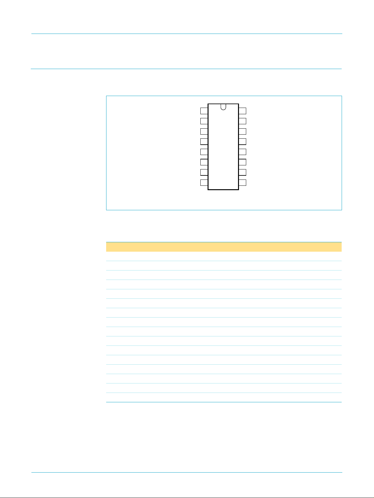
The TDA8942P comes in a 16-pin dual in-line (DIP) package.The TDA8942P is
printed-circuit board (PCB) compatible with all other types in the TDA894x family.
One PCB footprint accommodates both the mono and the stereo products.
2. Features
■ Few external components
■ Fixed gain
■ Standby and mute mode
■ No on/off switching plops
■ Low standby current
■ High supply voltage ripple rejection
■ Outputs short-circuit protected to ground, supply and across the load
c
c
■ Thermally protected
■ Printed-circuit board compatible.
3. Applications
■ Mains fed applications (e.g. TV sound)
■ PC audio
■ Portable audio.
4. Quick reference data
Table 1: Quick reference data
Symbol Parameter Conditions Min Typ Max Unit
V
CC
I
q
I
stb
supply voltage 6 9 18 V
quiescent supply current VCC=12V; RL= ∞ - 2232mA
standby supply current - - 10 µA
Philips Semiconductors
TDA8942P
2 x 1.5 W stereo BTL audio amplifier
Table 1: Quick reference data
Symbol Parameter Conditions Min Typ Max Unit
P
o
THD total harmonic distortion P
G
v
SVRR supply voltage ripple
5. Ordering information
Table 2: Ordering information
Type number Package
TDA8942P DIP16 plastic dual in-line package; 16 leads (300 mil);
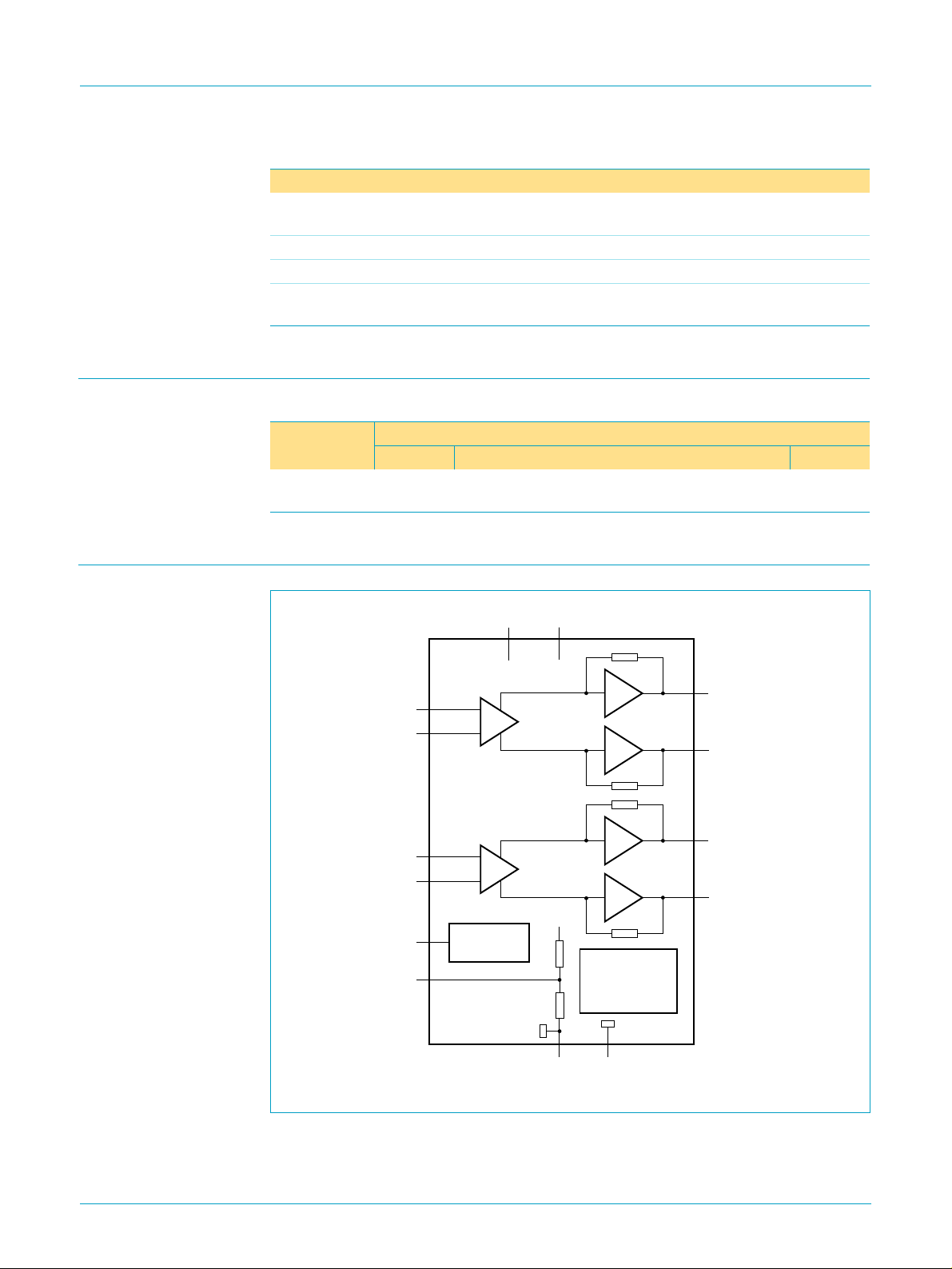
6. Block diagram
dth
…continued
output power THD = 10%;RL=16Ω;
=9V
V
CC
= 0.5 W - 0.03 0.3 %
o
1.2 1.5 - W
voltage gain 31 32 33 dB
50 65 - dB
rejection
Name Description Version
SOT38-1
long body
CC1
V
CC2
V
IN1−
IN1+
IN2−
IN2+
MODE
SVR
Fig 1. Block diagram.
13
3
12
11
4
STANDBY/
MUTE LOGIC
14
1
TDA8942P
9
V
CC
20
kΩ
SHORT CIRCUIT
TEMPERATURE
20
kΩ
GND18GND2
PROTECTION
16
AND
15
10
MGL578
OUT1−
2
OUT1+
7
OUT2−
OUT2+
9397 750 06862
© Philips Electronics N.V. 2000. All rights reserved.
Product specification Rev. 02 — 14 March 2000 2 of 23
Philips Semiconductors
7. Pinning information
7.1 Pinning
TDA8942P
2 x 1.5 W stereo BTL audio amplifier
handbook, halfpage
V
CC1
OUT1+
IN1+
MODE
n.c.
n.c.
OUT2−
GND2
1
2
3
4
TDA8942P
5
6
7
8
MGR895
16
15
14
13
12
11
10
9
GND1
OUT1−
SVR
IN1−
IN2−
IN2+
OUT2+
V
CC2
Fig 2. Pin configuration.
7.2 Pin description
Table 3: Pin description
Symbol Pin Description
V
CC1
OUT1+ 2 positive loudspeaker terminal 1
IN1+ 3 positive input 1
MODE 4 mode selection input (standby, mute, operating)
n.c. 5 not connected
n.c. 6 not connected
OUT2− 7 negative loudspeaker terminal 2
GND2 8 ground channel 2
V
CC2
OUT2+ 10 positive loudspeaker terminal 2
IN2+ 11 positive input 2
IN2− 12 negative input 2
IN1− 13 negative input 1
SVR 14 half supply voltage decoupling (ripple rejection)
OUT1− 15 negative loudspeaker terminal 2
GND1 16 ground channel 1
1 supply voltage channel 1
9 supply voltage channel 2
9397 750 06862
Product specification Rev. 02 — 14 March 2000 3 of 23
© Philips Electronics N.V. 2000. All rights reserved.

Philips Semiconductors
8. Functional description
The TDA8942P is a stereo BTL audio power amplifier capable of delivering 2 × 1.5 W
output power to a 16 Ω load at THD = 10%, using a 9 V power supply. The voltage
gain is fixed at 32 dB.
With the three-level MODE input the device can be switched from ‘standby’ to ‘mute’
and to ‘operating’ mode.
The TDA8942P outputs are protected by an internal thermal shutdown protection
mechanism and a short-circuit protection.
8.1 Input configuration
The TDA8942P inputs can be driven symmetrical (floating) as well as asymmetrical.
In the asymmetrical mode one input pin is connected via a capacitor to the signal
ground which should be as close as possible to the SVR (electrolytic) capacitor
ground. Note that the DC level of the input pins is half of the supply voltage VCC, so
coupling capacitors for both pins are necessary.
TDA8942P
2 x 1.5 W stereo BTL audio amplifier
The input cut-off frequency is:
f
i cut off–()
For Ri=45kΩ and Ci= 220 nF:
f
i cut off–()
As shown in Equation 1 and 2, large capacitor values for the inputs are not
necessary; so the switch-on delay during charging of the input capacitors, can be
minimized. This results in a good low frequency response and good switch-on
behaviour.
Remark: To prevent HF oscillations do not leave the inputs open, connect a capacitor
of at least 1.5 nF across the input pins close to the device.
=
1
---------------------------- -
2π RiCi×()
---------------------------------------------------------------- -
2π 45 103× 220× 109–×()
1
16 Hz==
(1)
(2)
9397 750 06862
Product specification Rev. 02 — 14 March 2000 4 of 23
© Philips Electronics N.V. 2000. All rights reserved.

Philips Semiconductors
8.2 Power amplifier
The power amplifier is a Bridge Tied Load (BTL) amplifier with an all-NPN output
stage, capable of delivering a peak output current of 2 A.
The BTL principle offers the following advantages:
•
•
•
•
8.2.1 Output power measurement
The output power as a function of the supply voltage is measured on the output pins
at THD = 10%; see Figure 8. The maximum output power is limited by the maximum
powerdissipation in the plastic dual in-line (DIP16) package.See also Section 14.2 on
page 16.
8.2.2 Headroom
TDA8942P
2 x 1.5 W stereo BTL audio amplifier
Lower peak value of the supply current
The ripple frequency on the supply voltage is twice the signal frequency
No expensive DC-blocking capacitor
Good low frequency performance.
Typical CD music requires at least 12 dB (factor 15.85) dynamic headroom –
compared to the average power output – for transferring the loudest parts without
distortion. At VCC=9V, RL=16Ω and Po= 1 W at THD = 1% (see Figure 6a), the
Average Listening Level (ALL) – music power – without any distortion yields:
P
= 1 W/15.85 = 63 mW.
o(ALL)
The power dissipation can be derived from Figure 11 on page 11 for 0 dB
respectively 12 dB headroom.
Table 4: Power rating as function of headroom
Headroom Power output (THD = 0.1%) Power dissipation (P)
0dB P
12 dB P
= 1 W 2.35 W
o
= 63 mW 1.15 W
o(ALL)
For the average listening level a power dissipation of 1.15 W can be used for
calculation of the maximum ambient temperature T
amb(max)
(see Section 14.2).
8.3 Mode selection
The TDA8942P has three functional modes, which can be selected by applying the
proper DC voltage to pin MODE. See Figure 4 and 5 for the respective DC levels,
which depend on the supply voltage level. The MODE pin can be driven by a 3-state
logic output stage: e.g. a microcontroller with additional components for DC-level
shifting.
Standby — In this mode the current consumption is very low and the outputs are
floating. The device is in standby mode when (VCC− 0.5 V) < V
MODE<VCC
, or when
the MODE pin is left floating (high impedance). The power consumption of the
TDA8942P will be reduced to <0.18 mW.
9397 750 06862
Product specification Rev. 02 — 14 March 2000 5 of 23
© Philips Electronics N.V. 2000. All rights reserved.

Philips Semiconductors
Mute — In this mode the amplifier is DC-biased but not operational (no audio output);
the DC level of the input and output pins remain on half the supply voltage. This
allows the input coupling and Supply Voltage Ripple Rejection (SVRR) capacitors to
be charged to avoid pop-noise. The device is in mute mode when
3V<V
Operating — In this mode the amplifier is operating normally. The operating mode is
activated at V
8.3.1 Switch-on and switch-off
To avoid audible plops during supply voltage switch-on or switch-off, the device is set
to standby mode before the supply voltage is applied (switch-on) or removed
(switch-off).
The switch-on and switch-off time can be influenced by an RC-circuit on the MODE
pin. Rapid on/off switching of the device or the MODE pin may cause ‘click- and
pop-noise’. This can be prevented by proper timing of the RC-circuit on the MODE
pin.
<(VCC− 1.5 V).
MODE
MODE
TDA8942P
2 x 1.5 W stereo BTL audio amplifier
< 0.5 V.
8.4 Supply Voltage Ripple Rejection (SVRR)
The SVRR is measured with an electrolytic capacitor of 10 µF on pin SVR at a
bandwidth of 10 Hz to 80 kHz. Figure 13 on page 12 illustrates the SVRR as function
of the frequency.A larger capacitor value on the SVR pin improves the ripple rejection
behaviour at the lower frequencies.
8.5 Built-in protection circuits
The TDA8942P contains two types of protection circuits, i.e. short-circuit and thermal
shutdown.
8.5.1 Short-circuit protection
Short-circuit to ground or supply line — This is detected by a so-called ‘missing
current’ detection circuit which measures the current in the positive supply line and
the current in the ground line. A difference between both currents larger than 0.4 A,
switches the power stage to standby mode (high impedance).
Short-circuit across the load — This is detected by an absolute-current
measurement. An absolute-current larger than 2 A, switches the power stage to
standby mode (high impedance).
8.5.2 Thermal shutdown protection
The junction temperature is measured by a temperature sensor; at a junction
temperature of approximately 150 °C this detection circuit switches the power stage
to standby mode (high impedance).
9397 750 06862
Product specification Rev. 02 — 14 March 2000 6 of 23
© Philips Electronics N.V. 2000. All rights reserved.

Philips Semiconductors
TDA8942P
2 x 1.5 W stereo BTL audio amplifier
9. Limiting values
Table 5: Limiting values
In accordance with the Absolute Maximum Rating System (IEC 60134).
Symbol Parameter Conditions Min Max Unit
V
CC
supply voltage no signal −0.3 +25 V
operating −0.3 +18 V
V
I
I
ORM
T
stg
T
amb
P
tot
V
CC(sc)
input voltage −0.3 VCC+ 0.3 V
repetitive peak output current - 2 A
storage temperature non-operating −55 +150 °C
operating ambient temperature −40 +85 °C
total power dissipation - 2.2 W
supplyvoltage to guaranteeshort-circuit
-12V
protection
10. Thermal characteristics
Table 6: Thermal characteristics
Symbol Parameter Conditions Value Unit
R
th(j-a)
thermal resistance from junction to ambient in free air 57 K/W
11. Static characteristics
Table 7: Static characteristics
VCC=12V; T
Symbol Parameter Conditions Min Typ Max Unit
V
CC
I
q
I
stb
V
O
[3]
∆V
OUT
V
MODE
I
MODE
[1] With a load connected at the outputs the quiescent current will increase, the maximum of this increase being equal to the differential
output voltage offset (∆V
[2] The DC output voltage with respect to ground is approximately 0.5VCC.
[3] ∆V
OUT
=25°C; RL=8Ω; V
amb
supply voltage operating 6 9 18 V
quiescent supply current RL= ∞
standby supply current V
DC output voltage
differential output voltage offset - - 200 mV
mode selection input voltage operating mode 0 - 0.5 V
mode selection input current 0 < V
= V
OUT+
− V
=0V; Vi= 0 V; measured in test circuit Figure 14; unless otherwise specified.
MODE
) divided by the load resistance (RL).
OUT
OUT−
[1]
- 2232mA
MODE=VCC
--10µA
[2]
- 4.5 - V
mute mode 3 - V
standby mode V
MODE<VCC
− 0.5 - V
CC
--20µA
− 1.5 V
CC
CC
V
9397 750 06862
Product specification Rev. 02 — 14 March 2000 7 of 23
© Philips Electronics N.V. 2000. All rights reserved.
 Loading...