

Philips TDA8927TH, TDA8927J Datasheet

INTEGRATED CIRCUITS
DATA SH EET
TDA8927
Power stage 2 × 80 W class-D
audio amplifier
Objective specification
File under Integrated Circuits, IC01
2001 Dec 11

Philips Semiconductors Objective specification
Power stage 2 × 80 W class-D
audio amplifier
CONTENTS
1 FEATURES
2 APPLICATIONS
3 GENERAL DESCRIPTION
4 QUICK REFERENCE DATA
5 ORDERING INFORMATION
6 BLOCK DIAGRAMS
7 PINNING INFORMATION
8 FUNCTIONAL DESCRIPTION
8.1 Power stage
8.2 Protections
8.2.1 Overtemperature
8.2.2 Short-circuit across the loudspeaker terminals
8.3 BTL operation
9 LIMITING VALUES
10 THERMAL CHARACTERISTICS
11 QUALITY SPECIFICATION
12 DC CHARACTERISTICS
13 AC CHARACTERISTICS
14 SWITCHING CHARACTERISTICS
14.1 Duty factor
TDA8927
15 TEST AND APPLICATION INFORMATION
15.1 BTL application
15.2 Remarks
15.3 Output power
15.4 Reference designs
15.5 Reference design bill of material
15.6 Curves measured in reference design
16 PACKAGE OUTLINES
17 SOLDERING
17.1 Introduction
17.2 Through-hole mount packages
17.2.1 Soldering by dipping or by solder wave
17.2.2 Manual soldering
17.3 Surface mount packages
17.3.1 Reflow soldering
17.3.2 Wave soldering
17.3.3 Manual soldering
17.4 Suitability of IC packages for wave,reflow and
dipping soldering methods
18 DATA SHEET STATUS
19 DEFINITIONS
20 DISCLAIMERS
2001 Dec 11 2

Philips Semiconductors Objective specification
Power stage 2 × 80 W class-D
audio amplifier
1 FEATURES
• High efficiency (>94%)
• Operating voltage from ±15 to ±30 V
• Very low quiescent current
• High output power
• Short-circuit proof across the load, only in combination
with controller TDA8929T
• Diagnostic output
• Usable as a stereo Single-Ended (SE) amplifier or as a
mono amplifier in Bridge-Tied Load (BTL)
• Electrostatic discharge protection (pin to pin)
• Thermally protected, only in combination with controller
TDA8929T.
2 APPLICATIONS
• Television sets
• Home-sound sets
TDA8927
• Multimedia systems
• All mains fed audio systems
• Car audio (boosters).
3 GENERAL DESCRIPTION
The TDA8927 is the switching power stage of a two-chip
set for a high efficiency class-D audio power amplifier
system. The system is split into two chips:
• TDA8927J/ST/TH; a digital power stage in a DBS17P,
RDBS17P or HSOP24 power package
• TDA8929T; the analog controller chip in a SO24
package.
With this chip set a compact 2 × 80 W audio amplifier
systemcanbebuilt,operatingwithhighefficiencyand very
low dissipation. No heatsink is required, or depending on
supply voltage and load, a very small one. The system
operates over a wide supply voltage range from
±15 up to ±30 V and consumes a very low quiescent
current.
4 QUICK REFERENCE DATA
SYMBOL PARAMETER CONDITIONS MIN. TYP. MAX. UNIT
General; VP= ±25 V
V
P
I
q(tot)
η efficiency P
supply voltage ±15 ±25 ±30 V
total quiescent current no load connected − 35 45 mA
=30W − 94 − %
o
Stereo single-ended configuration
P
o
output power RL=4Ω; THD = 10%; VP= ±25 V 60 65 − W
R
=4Ω; THD = 10%; VP= ±27 V 74 80 − W
L
Mono bridge-tied load configuration
P
o
output power RL=4Ω; THD = 10%; VP= ±17 V 90 110 − W
R
=8Ω; THD = 10%; VP= ±25 V 120 150 − W
L
5 ORDERING INFORMATION
PACKAGE
TYPE NUMBER
NAME DESCRIPTION VERSION
TDA8927J DBS17P plastic DIL-bent-SIL power package; 17 leads (lead length
12 mm)
TDA8927ST RDBS17P plastic rectangular-DIL-bent-SIL power package; 17 leads (row
spacing 2.54 mm)
TDA8927TH HSOP24 plastic, heatsink small outline package; 24 leads; low stand-off
height
SOT243-1
SOT577-1
SOT566-2
2001 Dec 11 3
Philips Semiconductors Objective specification
Power stage 2 × 80 W class-D
audio amplifier
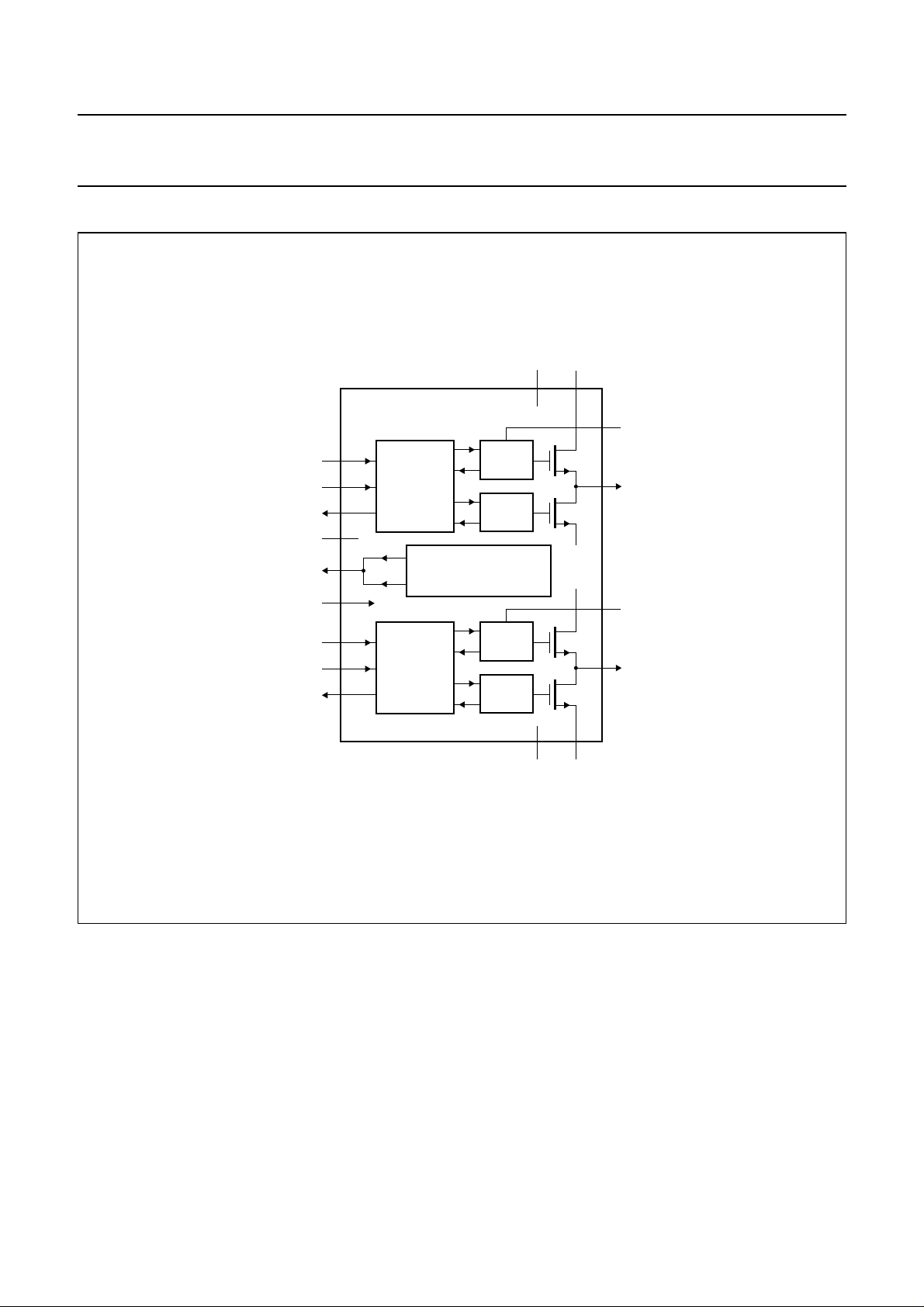
6 BLOCK DIAGRAMS
handbook, full pagewidth
EN1
SW1
REL1
STAB
DIAG
POWERUP
EN2
SW2
REL2
4
1
2
9
3
15
14
17
16
TDA8927J
TDA8927ST
CONTROL
AND
HANDSHAKE
temp
TEMPERATURE SENSOR
current
CURRENT PROTECTION
CONTROL
AND
HANDSHAKE
AND
DRIVER
HIGH
DRIVER
LOW
DRIVER
HIGH
DRIVER
LOW
V
DD2VDD1
13 5
V
V
SS1
DD2
TDA8927
6
BOOT1
7
OUT1
12
BOOT2
11
OUT2
810
V
SS1VSS2
MGW138
Fig.1 Block diagram of TDA8927J and TDA8927ST.
2001 Dec 11 4
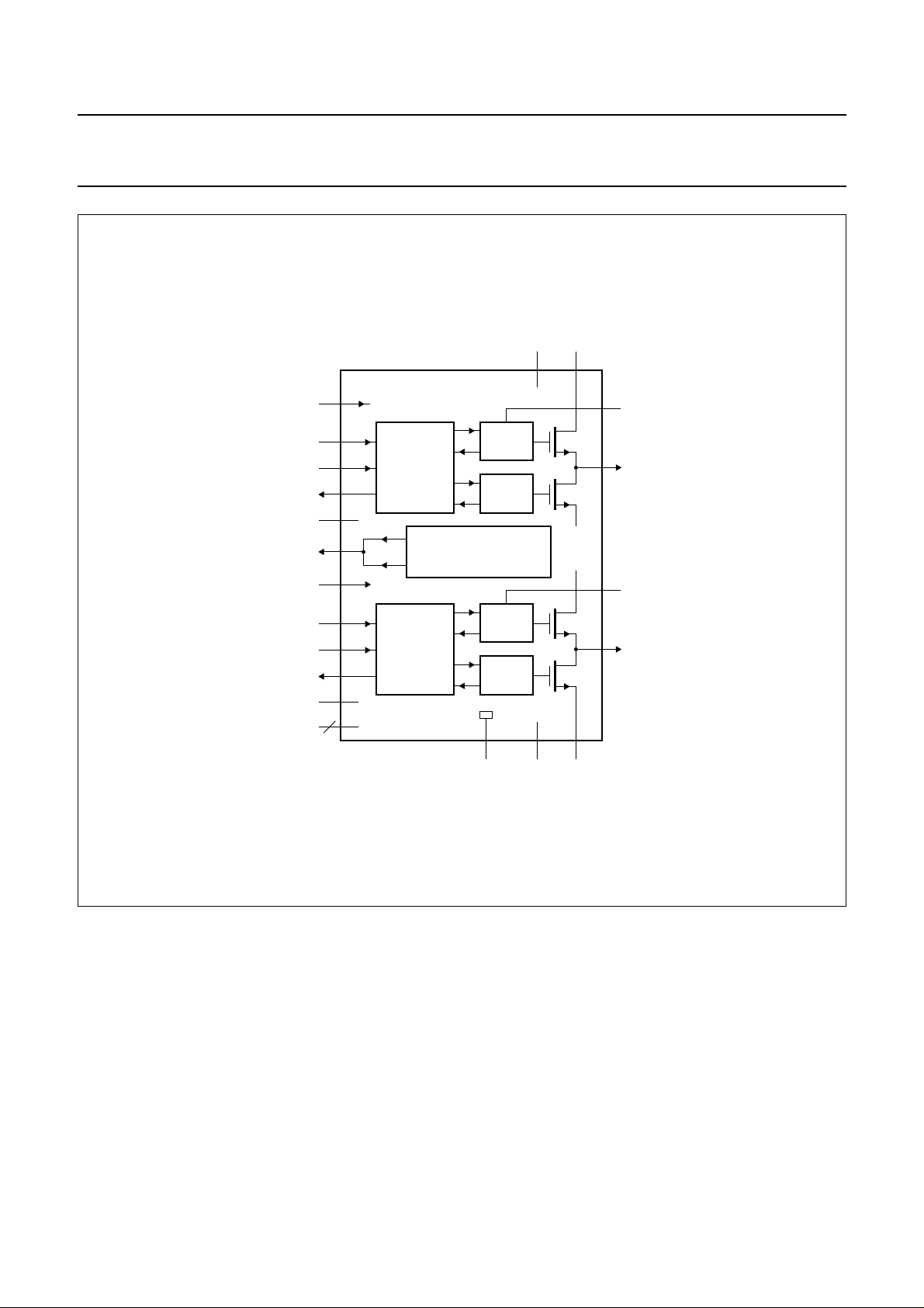
Philips Semiconductors Objective specification
Power stage 2 × 80 W class-D
audio amplifier
handbook, full pagewidth
LIM
EN1
SW1
REL1
STAB
DIAG
POWERUP
EN2
SW2
REL2
STAB
n.c.
17
24
21
22
6
23
14
13
16
15
7
4
1, 12, 18, 20
TDA8927TH
CONTROL
AND
HANDSHAKE
temp
TEMPERATURE SENSOR
current
CURRENT PROTECTION
CONTROL
AND
HANDSHAKE
DRIVER
HIGH
DRIVER
LOW
AND
DRIVER
HIGH
DRIVER
LOW
19 5 8
V
SS(sub)
V
DD2VDD1
11 2
V
V
V
SS1VSS2
SS1
DD2
TDA8927
3
BOOT1
4
OUT1
10
BOOT2
9
OUT2
MGW140
Fig.2 Block diagram of TDA8927TH.
2001 Dec 11 5

Philips Semiconductors Objective specification
Power stage 2 × 80 W class-D
TDA8927
audio amplifier
7 PINNING INFORMATION
SYMBOL
SW1 1 1 21 digital switch input channel 1
n.c. −−1 not connected
REL1 2 2 22 digital control output channel 1
DIAG 3 3 23 digital open-drain output for overtemperature and
EN1 4 4 24 digital enable input for channel 1
V
DD1
BOOT1 6 6 3 bootstrap capacitor channel 1
STAB −−6 decoupling internal stabilizer for logic supply
OUT1 7 7 4 PWM output channel 1
STAB −−7 decoupling internal stabilizer for logic supply
V
SS1
STAB 9 9 − decoupling internal stabilizer for logic supply
V
SS2
OUT2 11 11 9 PWM output channel 2
BOOT2 12 12 10 bootstrap capacitor channel 2
n.c. −−12 not connected
V
DD2
EN2 14 14 13 digital enable input for channel 2
POWERUP 15 15 14 enable input for switching-on internal reference
REL2 16 16 15 digital control output channel 2
SW2 17 17 16 digital switch input channel 2
LIM −−17 current input for setting maximum load current limit
n.c. −−18 not connected
V
SS(sub)
n.c. −−20 not connected
TDA8927J TDA8927ST TDA8927TH
5 5 2 positive power supply channel 1
8 8 5 negative power supply channel 1
10 10 8 negative power supply channel 2
13 13 11 positive power supply channel 2
−−19 negative supply (substrate)
PIN
DESCRIPTION
overcurrent report
sources
2001 Dec 11 6

Philips Semiconductors Objective specification
Power stage 2 × 80 W class-D
audio amplifier
handbook, halfpage
SW1
REL1
DIAG
EN1
V
DD1
BOOT1
OUT1
V
SS1
STAB
V
SS2
OUT2
BOOT2
V
DD2
EN2
POWERUP
REL2
SW2
1
2
3
4
5
6
7
8
9
TDA8927ST
10
11
12
13
14
15
16
17
TDA8927J
handbook, halfpage
EN1
DIAG
REL1
SW1
n.c.
V
SS(sub)
n.c.
LIM
SW2
REL2
POWERUP
EN2
TDA8927
24
23
22
21
20
19
18
17
16
15
14
13
TDA8927TH
MGW144
1
2
3
4
5
6
7
8
9
10
11
12
n.c.
V
DD1
BOOT1
OUT1
V
SS1
STAB
STAB
V
SS2
OUT2
BOOT2
V
DD2
n.c.
MGW142
Fig.3 Pin configuration of TDA8927J and
TDA8927ST.
2001 Dec 11 7
Fig.4 Pin configuration of TDA8927TH.

Philips Semiconductors Objective specification
Power stage 2 × 80 W class-D
audio amplifier
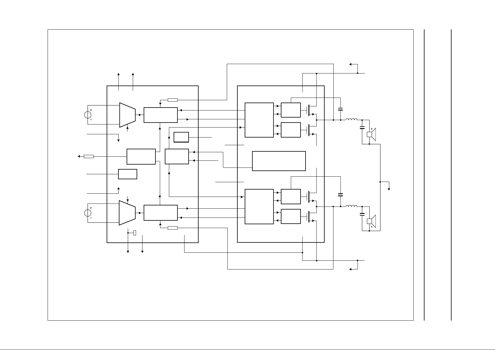
8 FUNCTIONAL DESCRIPTION
The combination of the TDA8927J and the TDA8929T
produces a two-channel audio power amplifier system
usingthe class-D technology (seeFig.5).In the TDA8929T
controllerdevice the analog audio input signal is converted
into a digital Pulse Width Modulation (PWM) signal.
ThepowerstageTDA8927isusedfordrivingthe low-pass
filter and the loudspeaker load. It performs a level shift
from the low-power digital PWM signal, at logic levels, to a
high-power PWM signal that switchs between the main
supply lines. A second-order low-pass filter converts the
PWM signal into an analog audio signal across the
loudspeaker.
See the specification of the TDA8929T for a description of
the controller.
8.1 Power stage
The power stage contains the high-power DMOS
switches,the drivers, timing and handshaking betweenthe
power switches and some control logic. For protection, a
temperature sensor and a maximum current detector are
built-in on the chip.
For interfacing with the controller chip the following
connections are used:
• Switch (pins SW1 and SW2): digital inputs; switching
from VSS to VSS+ 12 V and driving the power DMOS
switches
• Release (pins REL1 and REL2): digital outputs to
indicate switching from VSS to VSS+ 12 V, follows
pins SW1 and SW2 with a small delay
• Enable (pins EN1 and EN2): digital inputs; at a level of
VSSthe power DMOS switches are open and the PWM
output is floating; at a level of VSS+ 12 V the power
stage is operational and controlled by the switch pin if
pin POWERUP is at VSS+12V
• Power-up (pin POWERUP): must be connected to a
continuous supply voltage of at least VSS+ 5 V with
respect to V
• Diagnostics(pin DIAG):digitalopen-drain output; pulled
to VSS if temperature or maximum current is exceeded.
SS
TDA8927
8.2 Protections
Temperature and short-circuit protection sensors are
included in the TDA8927 power stage. These protections
are only operational in combination with the TDA8929T. In
the event that the maximum current or maximum
temperature is exceeded the diagnostic output is
activated.The controller has to take appropriate measures
by shutting down the system.
8.2.1 OVERTEMPERATURE
If the junction temperature (Tj) exceeds 150 °C, then
pin DIAG becomes LOW. The diagnostic pin is released if
the temperature is dropped to approximately 130 °C, so
there is a hysteresis of approximately 20 °C.
8.2.2 SHORT-CIRCUIT ACROSS THE LOUDSPEAKER
TERMINALS
When the loudspeaker terminals are short-circuited it will
be detected by the current protection. If the output current
exceeds the maximum output current of 7.5 A, then
pin DIAG becomes LOW. The controller should shut down
the system to prevent damage. Using the TDA8929T the
system is shut down within 1 µs, and after 220 ms, it will
attempt to restart the system again. During this time the
dissipation is very low, so the average dissipation during a
short-circuit is practically zero.
For the TDA8927TH the limit value can be externally
adjusted using a resistor. For the maximum value of 7.5 A
pin LIM should be connected to VSS. When a resistor R
is connected between pin LIM and VSS the maximum
output current can be set at a lower value, using:
I
O(max)
Example 1: with R
2.1 105×
=
--------------------------------R
ext
28 kΩ+
=27kΩ the current is limited at
ext
3.8 A.
Example 2: with R
=0Ω the current is limited at 7.5 A.
ext
In the TDA8927J and the TDA8927ST pin LIM is internally
connected to VSS, so I
O(max)
= 7.5 A.
ext
2001 Dec 11 8
This text is here in white to force landscape pages to be rotated correctly when browsing through the pdf in the Acrobat reader.This text is here in
_white to force landscape pages to be rotated correctly when browsing through the pdf in the Acrobat reader.This text is here inThis text is here in
white to force landscape pages to be rotated correctly when browsing through the pdf in the Acrobat reader. white to force landscape pages to be ...
2001 Dec 11 9
V
OUT1
BOOT2
OUT2
DDA
BOOT1
V
SSA
+25 V
−25 V
MGU388
V
SSA
V
V
i(1)
MODE
V
i(2)
R
OSC
IN1−
IN1+
SGND1
OSC
MODE
SGND2
IN2+
IN2−
V
SSAVDDA
4
5
2
SGND
7
6
SGND
11
8
9
V
SS2(sub)
V
SS1VDD1
3
1
TDA8929T
INPUT
STAGE
mute
OSCILLATOR
MODE
mute
INPUT
STAGE
12 10
V
SSAVDDA
PWM
MODULATOR
PWM
MODULATOR
V
DD2
R
fb
STABI
MANAGER
R
fb
18
V
20
23
24
21
19
22
15
16
13
14
17
SSD
PWM1
REL1
SW1
EN1
STAB
DIAGCUR
DIAGTMP
EN2
SW2
REL2
PWM2
REL1
SW1
EN1
STAB
DIAG
POWERUP
EN2
SW2
REL2
TDA8927J
2
CONTROL
1
AND
4
HANDSHAKE
9
TEMPERATURE SENSOR
3
CURRENT PROTECTION
15
14
CONTROL
17
AND
HANDSHAKE
16
AND
DRIVER
HIGH
DRIVER
LOW
DRIVER
HIGH
DRIVER
LOW
V
DDD
V
DD2VDD1
13 5
6
7
V
SS1
V
DD2
12
11
810
V
V
SS2
SS1
V
SSD
SGND
(0 V)
Philips Semiconductors Objective specification
Power stage 2 × 80 W class-D
audio amplifier
TDA8927
Fig.5 Typical application schematic of the class-D system using TDA8929T and the TDA8927J.
handbook, full pagewidth
Philips Semiconductors Objective specification
Power stage 2 × 80 W class-D
audio amplifier
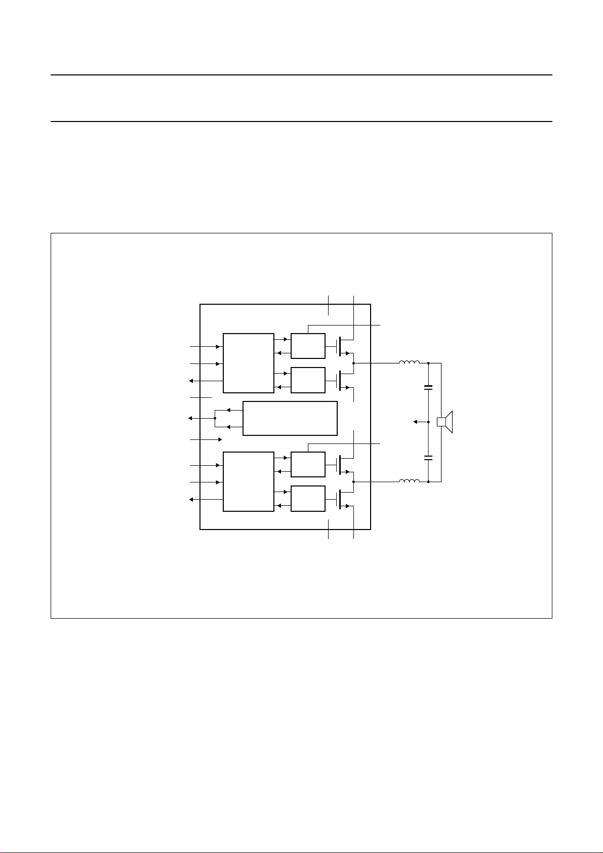
8.3 BTL operation
BTL operation can be achieved by driving the audio input
channels of the controller in the opposite phase and by
connecting the loudspeaker with a BTL output filter
between the two PWM output pins of the power stage
(see Fig.6).
handbook, full pagewidth
TDA8927J
4
EN1
SW1
REL1
STAB
DIAG
POWERUP
EN2
SW2
REL2
1
2
9
3
15
14
17
16
CONTROL
AND
HANDSHAKE
temp
TEMPERATURE SENSOR
current
CURRENT PROTECTION
CONTROL
AND
HANDSHAKE
AND
TDA8927
In this way the system operates as a mono BTL amplifier
and with the same loudspeaker impedance a four times
higher output power can be obtained.
For more information see Chapter 15.
V
DD2VDD1
13 5
6
BOOT1
DRIVER
HIGH
DRIVER
LOW
DRIVER
HIGH
DRIVER
LOW
V
V
SS1
DD2
OUT1
7
SGND
(0 V)
12
BOOT2
OUT2
11
Fig.6 Mono BTL application.
2001 Dec 11 10
810
V
SS1VSS2
MGU386

Philips Semiconductors Objective specification
Power stage 2 × 80 W class-D
TDA8927
audio amplifier
9 LIMITING VALUES
In accordance with the Absolute Maximum Rate System (IEC 60134).
SYMBOL PARAMETER CONDITIONS MIN. MAX. UNIT
V
P
V
P(sc)
I
ORM
T
stg
T
amb
T
vj
V
es(HBM)
V
es(MM)
supply voltage −±30 V
supply voltage for
−±30 V
short-circuits across the load
repetitive peak current in
− 7.5 A
output pins
storage temperature −55 +150 °C
ambient temperature −40 +85 °C
virtual junction temperature − 150 °C
electrostatic discharge
voltage (HBM)
note 1
all pins with respect to V
all pins with respect to V
(class A) −500 +500 V
DD
(class A1) −1500 +1500 V
SS
all pins with respect to each other
−1500 +1500 V
(class A1)
electrostatic discharge
voltage (MM)
note 2
all pins with respect to V
all pins with respect to V
(class B) −250 +250 V
DD
(class B) −250 +250 V
SS
all pins with respect to each other
−250 +250 V
(class B)
Notes
1. Human Body Model (HBM); R
= 1500 Ω; C = 100 pF.
s
2. Machine Model (MM); Rs=10Ω; C = 200 pF; L = 0.75 µH.
10 THERMAL CHARACTERISTICS
SYMBOL PARAMETER CONDITIONS VALUE UNIT
R
th(j-a)
thermal resistance from junction to ambient in free air
TDA8927J 40 K/W
TDA8927ST 40 K/W
TDA8927TH 40 K/W
R
th(j-c)
thermal resistance from junction to case in free air
TDA8927J ≈1.0 K/W
TDA8927ST ≈1.0 K/W
TDA8927TH 1 K/W
11 QUALITY SPECIFICATION
In accordance with
“SNW-FQ611-part D”
if this type is used as an audio amplifier.
2001 Dec 11 11
 Loading...