

Page 1

INTEGRATED CIRCUITS
DATA SH EET
TDA8925
Power stage2x15to25Wclass-D
audio amplifier
Product specification
Supersedes data of 2004 Jan 05
2004 May 06
Page 2

Philips Semiconductors Product specification
Power stage 2 x 15 to 25 W class-D
audio amplifier
CONTENTS
1 FEATURES
2 APPLICATIONS
3 GENERAL DESCRIPTION
4 QUICK REFERENCE DATA
5 ORDERING INFORMATION
6 BLOCK DIAGRAM
7 PINNING
8 FUNCTIONAL DESCRIPTION
8.1 Power stage
8.2 Protection
8.2.1 Overtemperature
8.2.2 Short-circuit across the loudspeaker terminals
9 LIMITING VALUES
10 THERMAL CHARACTERISTICS
11 QUALITY SPECIFICATION
12 DC CHARACTERISTICS
13 AC CHARACTERISTICS
14 SWITCHING CHARACTERISTICS
TDA8925
15 TEST AND APPLICATION INFORMATION
15.1 SE application
15.2 Package ground connection
15.3 Output power
15.4 Reference design
15.5 Reference design bill of material
15.5.1 Version 2; revision 5
15.5.2 Printed-circuit board
15.6 Curves measured in reference design
16 PACKAGE OUTLINES
17 SOLDERING
17.1 Introduction to soldering through-hole mount
packages
17.2 Soldering by dipping or by solder wave
17.3 Manual soldering
17.4 Suitability of through-hole mount IC packages
for dipping and wave soldering methods
18 DATA SHEET STATUS
19 DEFINITIONS
20 DISCLAIMERS
2004 May 06 2
Page 3

Philips Semiconductors Product specification
Power stage 2 x 15 to 25 W class-D
audio amplifier
1 FEATURES
• High efficiency (> 94 %)
• Operating voltage from ±7.5 V to ±30 V
• Very low quiescent current
• High output power
• Diagnostic output
• Usable as a stereo Single-Ended (SE) amplifier
• Electrostatic discharge protection (pin to pin)
• No heatsink required.
2 APPLICATIONS
• Television sets
• Home-sound sets
• Multimedia systems
• All mains fed audio systems.
TDA8925
3 GENERAL DESCRIPTION
The TDA8925 is a switching power stage for a high
efficiency class-D audio power amplifier system.
With this power stage a compact 2 × 15 W self oscillating
digital amplifier system can be built, operating with high
efficiency and very low dissipation. No heatsink is
required. Thesystem operates over a wide supply voltage
range from ±7.5 V up to ±30 V and consumes a very low
quiescent current.
4 QUICK REFERENCE DATA
SYMBOL PARAMETER CONDITIONS MIN. TYP. MAX. UNIT
General
V
P
I
q(tot)
η efficiency endstage Po= 15 W; RL=8Ω; VP= ±15 V − 94 − %
Stereo single-ended configuration
P
o
5 ORDERING INFORMATION
TYPE
NUMBER
TDA8925ST RDBS17P plastic rectangular-DIL-bent-SIL power package; 17 leads (row
TDA8925J DBS17P plastic DIL-bent-SIL power package; 17 leads (lead length
supply voltage ±7.5 ±15 ±30 V
total quiescent current no load connected; VP= ±15 V − 25 45 mA
output power RL=8Ω; THD = 10 %; VP= ±15 V 14 15 − W
RL=6Ω; THD = 10 %; VP= ±15 V − 20 − W
PACKAGE
NAME DESCRIPTION VERSION
SOT577-2
spacing 2.54 mm)
SOT243-3
7.7 mm)
2004 May 06 3
Page 4
Philips Semiconductors Product specification
Power stage 2 x 15 to 25 W class-D
audio amplifier
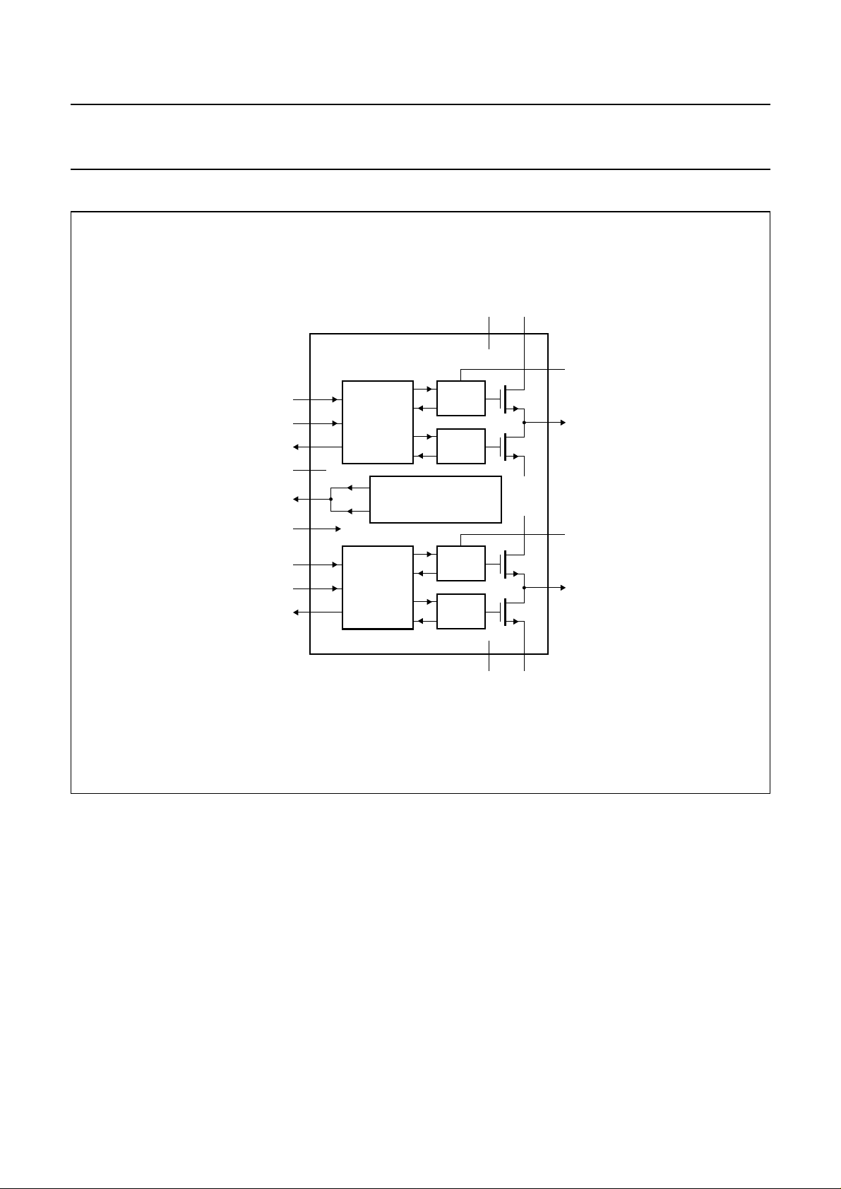
6 BLOCK DIAGRAM
handbook, full pagewidth
EN1
SW1
REL1
STAB
DIAG
POWERUP
EN2
SW2
REL2
4
1
2
9
3
15
14
17
16
CONTROL
HANDSHAKE
temp
current
CONTROL
HANDSHAKE
TDA8925
DRIVER
HIGH
AND
DRIVER
LOW
TEMPERATURE SENSOR
AND
CURRENT PROTECTION
DRIVER
HIGH
AND
DRIVER
LOW
V
DD2VDD1
13 5
V
V
SS1
DD2
TDA8925
6
BOOT1
7
OUT1
12
BOOT2
11
OUT2
Fig.1 Block diagram.
810
V
SS1VSS2
MDB610
2004 May 06 4
Page 5
Philips Semiconductors Product specification
Power stage 2 x 15 to 25 W class-D
audio amplifier
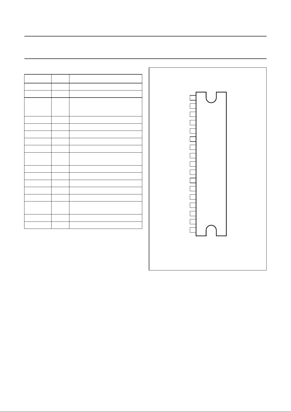
7 PINNING
SYMBOL PIN DESCRIPTION
SW1 1 digital switch input; channel 1
REL1 2 digital control output; channel 1
DIAG 3 digital open-drain output for
overtemperature and overcurrent
report
EN1 4 digital enable input; channel 1
V
DD1
BOOT1 6 bootstrap capacitor; channel 1
OUT1 7 PWM output; channel 1
V
SS1
STAB 9 decoupling internal stabilizer for
V
SS2
OUT2 11 PWM output; channel 2
BOOT2 12 bootstrap capacitor; channel 2
V
DD2
EN2 14 digital enable input; channel 2
POWERUP 15 enable input for switching on
REL2 16 digital control output; channel 2
SW2 17 digital switch input; channel 2
5 positive power supply; channel 1
8 negative power supply; channel 1
logic supply
10 negative power supply; channel 2
13 positive power supply; channel 2
internal reference sources
handbook, halfpage
POWERUP
SW1
REL1
DIAG
EN1
V
DD1
BOOT1
OUT1
V
SS1
STAB
V
SS2
OUT2
BOOT2
V
DD2
EN2
REL2
SW2
1
2
3
4
5
6
7
8
9
TDA8925ST/J
10
11
12
13
14
15
16
17
TDA8925
MDB611
Fig.2 Pin configuration.
2004 May 06 5
Page 6

Philips Semiconductors Product specification
Power stage 2 x 15 to 25 W class-D
audio amplifier
8 FUNCTIONAL DESCRIPTION
The TDA8925 is a two-channel audio power amplifier
system using the class-D technology (see Fig.1).
The power stage TDA8925S is used for driving the
loudspeaker load. It performs a level shift from the
low-power digital PWM signal, at logic levels, to a
high-power PWM signal that switches between the main
supplylines. A 2nd-order low-pass filter convertsthePWM
signal into an analog audio signal across the loudspeaker.
8.1 Power stage
The power stage contains the high-power DMOS
switches,thedrivers,timingandhandshakingbetweenthe
power switches and some control logic (see Fig.1). For
protection, a temperature sensor and a maximum current
detector are built-in on the chip.
The following functions are available:
• Switch (pins SW1 and SW2): digital inputs; switching
from VSS to VSS+ 12 V and driving the power DMOS
switches
• Release (pins REL1 and REL2): digital outputs;
switching from VSSto VSS+ 12 V; follow SW1 and SW2
with a small delay. Note: for self oscillating applications
this pin is not used.
• Power-up (pin POWERUP): must be connected to a
continuous supply voltage of at least VSS+ 5 V with
respect to V
• Enable (pins EN1 and EN2): digital inputs; at a level
of VSS the power DMOS switches are open and the
PWM outputs are floating; at a level of VSS+ 12 V the
power stage is operational
• Diagnostics(pin DIAG): digital open-drain output; pulled
to VSS if the temperature or maximum current is
exceeded.
SS
TDA8925
8.2 Protection
Temperature and short-circuit protection sensors are
included in the TDA8925. In the event that the maximum
current or maximum temperature is exceeded the
diagnostic output is pulled down to VSS. Since the
diagnostic is connected to the enable pins in the
application the system shuts down itself.
8.2.1 OVERTEMPERATURE
If the junction temperature (Tj) exceeds 150 °C, then
pin DIAG becomes LOW. The diagnostic pin is released if
the temperature is dropped to approximately 130 °C, so
there is a hysteresis of approximately 20 °C.
8.2.2 SHORT-CIRCUIT ACROSS THE LOUDSPEAKER
TERMINALS
When the loudspeaker terminals are short-circuited this
will be detected by the current protection. If the output
current exceeds the maximum output current of 3 A, then
pin DIAG becomes LOW. Using pin DIAG in combination
with the enable pins the system will shut down
immediately,andrestartagain.Theresultisthatthe output
current is limited at the overcurrent detection level.
2004 May 06 6
Page 7

Philips Semiconductors Product specification
Power stage 2 x 15 to 25 W class-D
TDA8925
audio amplifier
9 LIMITING VALUES
In accordance with the Absolute Maximum Rate System (IEC 60134).
SYMBOL PARAMETER CONDITIONS MIN. MAX. UNIT
V
P
V
P(sc)
I
ORM
T
stg
T
amb
T
vj
V
esd(HBM)
V
esd(MM)
supply voltage −±30 V
supply voltage for
−±30 V
short-circuits across the load
repetitive peak current in
− 3.5 A
output pins
storage temperature −55 +150 °C
ambient temperature −40 +85 °C
virtual junction temperature − 150 °C
electrostaticdischarge voltage
(HBM)
note 1
all pins with respect to VDD (class 1a) −500 +500 V
all pins with respect to VSS (class 1a) −1500 +1500 V
all pins with respect to each other
−1500 +1500 V
(class 1a)
electrostaticdischarge voltage
(MM)
note 2
all pins with respect to VDD (class B) −250 +250 V
all pins with respect to VSS (class B) −250 +250 V
all pins with respect to each other
−250 +250 V
(class B)
Notes
1. Human Body Model (HBM); Rs= 1500 Ω; C = 100 pF.
2. Machine Model (MM); Rs=10Ω; C = 200 pF; L = 0.75 µH.
10 THERMAL CHARACTERISTICS
SYMBOL PARAMETER CONDITIONS VALUE UNIT
R
R
th(j-a)
th(j-c)
thermal resistance from junction to ambient in free air 40 K/W
thermal resistance from junction to case in free air 1.5 K/W
11 QUALITY SPECIFICATION
In accordance with
“SNW-FQ611”
if this device is used as an audio amplifier.
2004 May 06 7
Page 8

Philips Semiconductors Product specification
Power stage 2 x 15 to 25 W class-D
TDA8925
audio amplifier
12 DC CHARACTERISTICS
VP= ±15 V; T
SYMBOL PARAMETER CONDITIONS MIN. TYP. MAX. UNIT
Supply
V
P
I
q(tot)
Internal stabilizer logic supply (pin STAB)
V
O(STAB)
Switch inputs (pins SW1 and SW2)
V
IH
V
IL
Control outputs (pins REL1 and REL2)
V
OH
V
OL
Diagnostic output (pin DIAG, open-drain)
V
OL
I
LO
Enable inputs (pins EN1 and EN2)
V
IH
V
IL
V
EN(hys)
I
I(EN)
Switching-on input (pin POWERUP)
V
POWERUP
I
I(POWERUP)
Temperature protection
T
diag
T
hys
Current protection
I
O(ocpl)
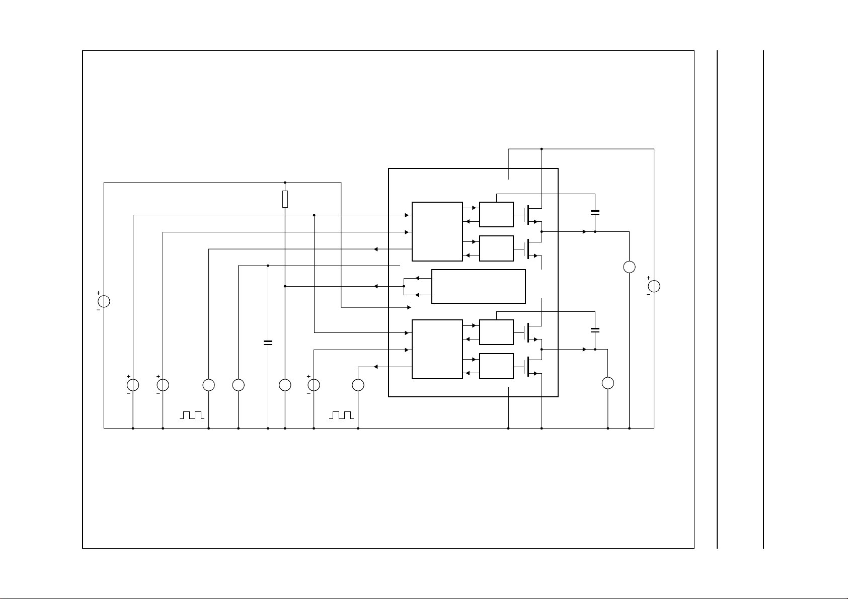
=25°C; measured in test diagram of Fig.4; unless otherwise specified.
amb
supply voltage ±7.5 ±15 ±30 V
total quiescent current no load connected − 25 45 mA
outputs floating − 510mA
stabilizer output voltage referenced to V
HIGH-level input voltage referenced to V
LOW-level input voltage referenced to V
HIGH-level output voltage referenced to V
LOW-level output voltage referenced to V
LOW-level output voltage I
= 1 mA; note 1 0 − 1.0 V
DIAG
SS
SS
SS
SS
SS
11.7 13 14.3 V
10 − 15 V
0 − 2V
10 − 15 V
0 − 2V
output leakage current no error condition −−50 µA
HIGH-level input voltage referenced to V
LOW-level input voltage referenced to V
SS
SS
9 − 15 V
05− V
hysteresis voltage − 4 − V
input current −−300 µA
operating voltage referenced to V
input current V
temperature activating diagnostic V
hysteresis on temperature
POWERUP
DIAG=VDIAG(LOW)
V
DIAG=VDIAG(LOW)
=12V − 100 170 µA
SS
5 − 12 V
150 −−°C
− 20 −°C
diagnostic
overcurrent protection level − 3.5 − A
Note
1. Temperature sensor or maximum current sensor activated.
2004 May 06 8
Page 9

Philips Semiconductors Product specification
Power stage 2 x 15 to 25 W class-D
TDA8925
audio amplifier
13 AC CHARACTERISTICS
VP= ±15 V; T
SYMBOL PARAMETER CONDITIONS MIN. TYP. MAX. UNIT
Single-ended application; note 1
P
o
THD total harmonic distortion Po= 1 W; note 3
η efficiency endstage Po=2× 15 W; fi= 1 kHz; note 4 − 94 − %
Notes
1. V
= ±15 V; RL=8Ω;fi= 1 kHz; f
P
in reference design (SE application) shown in Fig.5; unless otherwise specified.
2. Indirectly measured; based on R
3. Total Harmonic Distortion (THD) is measured in a bandwidth of 22 Hz to 20 kHz (AES 17 brickwall filter). When
distortion is measured using a low-order low-pass filter a significantly higher value will be found, due to the switching
frequency outside the audio band. Measured using the typical application circuit, given in Fig.5.
4. Efficiency for power stage.
=25°C; unless otherwise specified.
amb
output power RL=8Ω
= 310 kHz; Rs= 0.1 Ω (series resistance of filter coil); T
osc
measurement.
ds(on)
THD = 0.5 % 10
THD = 10 % 14
(2)
12 − W
(2)
15 − W
RL=6Ω
THD = 0.5 % − 16 − W
THD = 10 % − 20 − W
fi= 1 kHz − 0.05 0.1 %
fi= 10 kHz − 0.2 − %
=25°C; measured
amb
2004 May 06 9
Page 10
Philips Semiconductors Product specification
Power stage 2 x 15 to 25 W class-D
TDA8925
audio amplifier
14 SWITCHING CHARACTERISTICS
VP= ±15 V; T
SYMBOL PARAMETER CONDITIONS MIN. TYP. MAX. UNIT
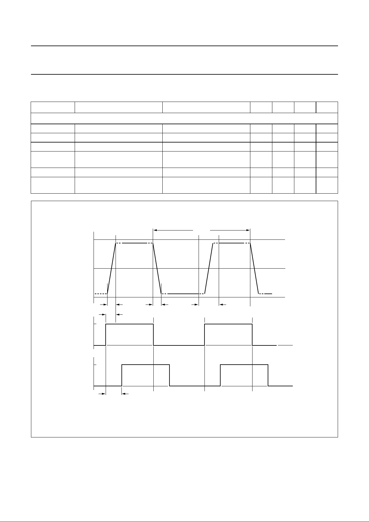
PWM outputs (pins OUT1 and OUT2); see Fig.3
t
r
t
f
t
blank
t
PD
t
W(min)
R
ds(on)
handbook, full pagewidth
=25°C; measured in Fig.4; unless otherwise specified.
amb
rise time − 30 − ns
fall time − 30 − ns
blanking time − 70 − ns
propagation delay from pin SW1 (SW2) to
− 200 − ns
pin OUT1 (OUT2)
minimum pulse width − 220 270 ns
on-resistance of the output
− 0.2 0.4 Ω
transistors
1/f
osc
V
DD
PWM
output
(V)
0 V
V
V
V
SW
(V)
V
REL
(V)
V
SS
STAB
V
SS
STAB
V
SS
t
r
t
PD
100 ns
t
f
t
blank
Fig.3 Timing diagram PWM output, switch and release signals.
MGW145
2004 May 06 10
Page 11
This text is here in white to force landscape pages to be rotated correctly when browsing through the pdf in the Acrobat reader.This text is here in
d
_white to force landscape pages to be rotated correctly when browsing through the pdf in the Acrobat reader.This text is here inThis text is here in
white to force landscape pages to be rotated correctly when browsing through the pdf in the Acrobat reader. white to force landscape pages to be ...
2004 May 06 11
12 V
12 kΩ
POWERUP
book, full pagewidth
EN1
4
SW1
1
REL1
2
STAB
9
DIAG
3
15
TDA8925
CONTROL
AND
HANDSHAKE
temp
TEMPERATURE SENSOR
current
CURRENT PROTECTION
AND
DRIVER
HIGH
DRIVER
LOW
V
DD2VDD1
13 5
V
SS1
V
DD2
BOOT1
6
15 nF
OUT1
7
V
V
OUT1
BOOT2
12
2V
15 TEST AND APPLICATION INFORMATION
audio amplifier
P
Philips Semiconductors Product specification
Power stage 2 x 15 to 25 W class-D
EN2
14
100
nF
V
V
V
V
V
EN
SW1
12 V
0
V
REL1
STAB
V
V
V
DIAG
12 V
SW2
0
SW2
REL2
V
V
REL2
17
16
CONTROL
AND
HANDSHAKE
DRIVER
HIGH
DRIVER
LOW
810
V
SS1
V
11
SS2
OUT2
V
OUT2
15 nF
V
MDB613
TDA8925
Fig.4 Test diagram.
Page 12

Philips Semiconductors Product specification
Power stage 2 x 15 to 25 W class-D
audio amplifier
15.1 SE application
For SE application the application diagram as shown in Fig.5 can be used.
15.2 Package ground connection
The heatsink of the TDA8925 is connected internally to VSS.
15.3 Output power
The output power in SE self oscillating class-D applications can be estimated using the formula
R
------------------------------------------RLR
o(1%)
=
-----------------------------------------------------------------
P
The maximum current should not exceed 3 A.
L
++
ds(on)Rs
2R
×
L
I
O(max)
Where:
RL= load impedance
Rs= series resistance of filter coil
P
= output power just at clipping.
o(1%)
The output power at THD = 10 %: P
2
V
×
P
=
------------------------------------------RLR
++
o(10%)
V
P
ds(on)Rs
= 1.25 × P
o(1%)
.
TDA8925
15.4 Reference design
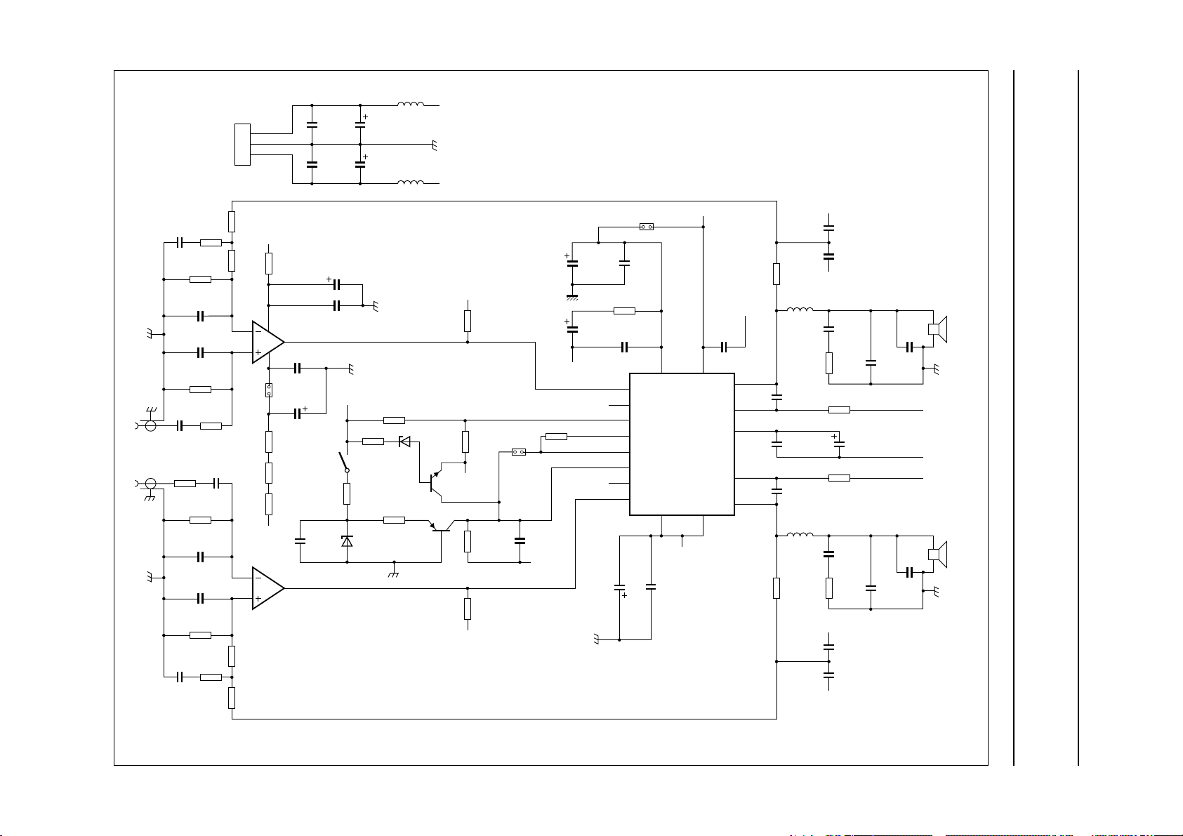
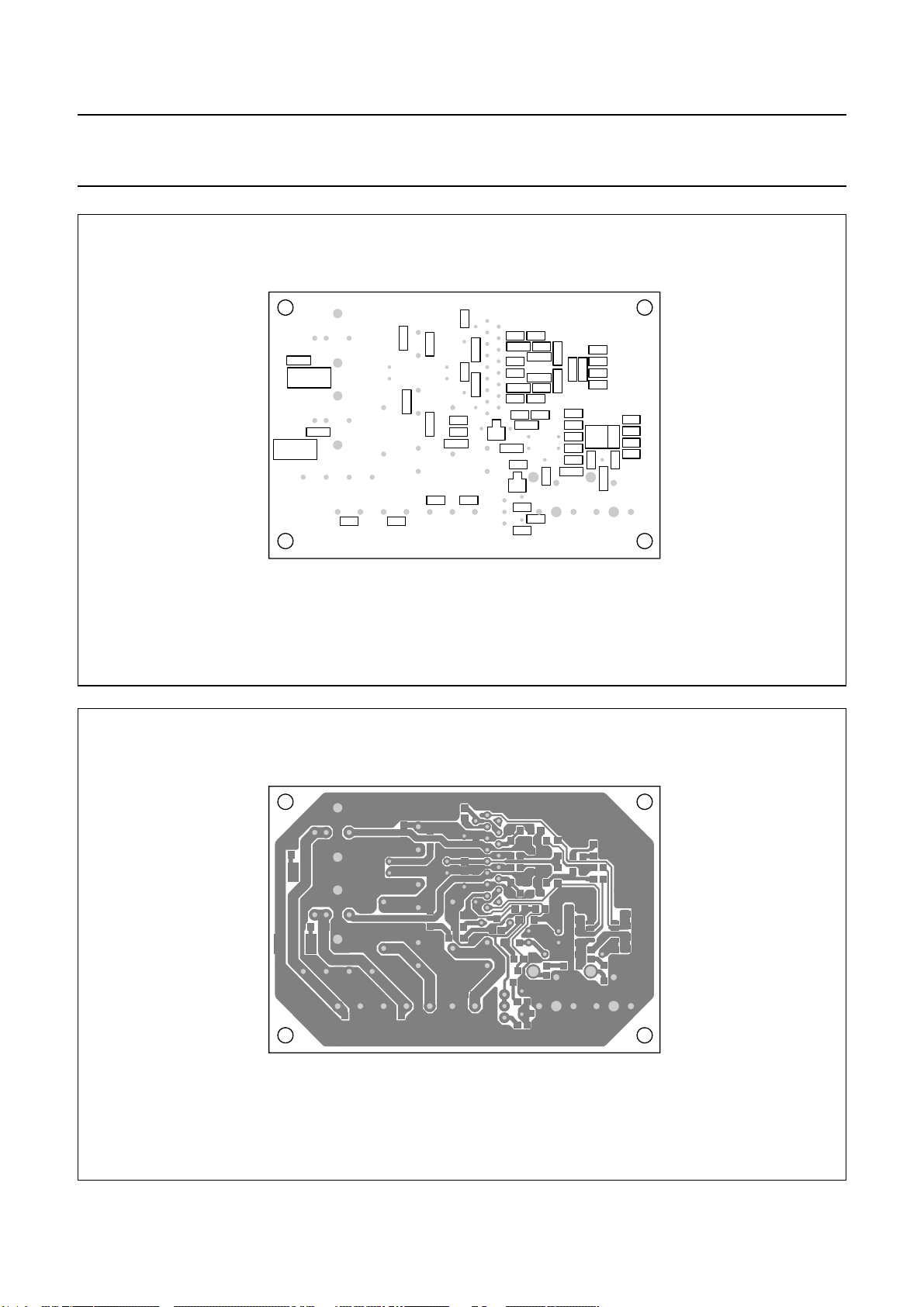
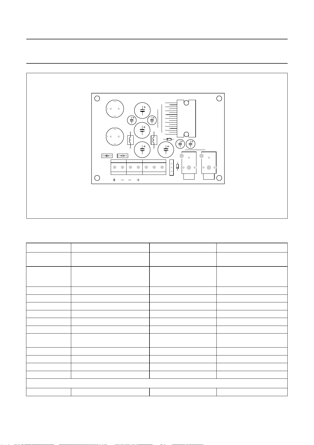
The reference design for a self oscillating class-D system for the TDA8925 is shown in Fig.5. The Printed-Circuit
Board (PCB) layout is shown in Figs 6, 7 and 8. The bill of materials is given in Section 15.5.1.
2004 May 06 12
Page 13
This text is here in white to force landscape pages to be rotated correctly when browsing through the pdf in the Acrobat reader.This text is here in
_white to force landscape pages to be rotated correctly when browsing through the pdf in the Acrobat reader.This text is here inThis text is here in
white to force landscape pages to be rotated correctly when browsing through the pdf in the Acrobat reader. white to force landscape pages to be ...
2004 May 06 13
L1
L2
Q1
BC856
Q2
V
DDP
V
SSP
STAB (U1,9)
R11
2 kΩ
R15
10 kΩ
V
SSP
R17
5.6 kΩ
R12
2 kΩ
STAB (U1,9)
J2
21
C37
220 pF
V
SSP
C5
C7
R24
0 Ω
V
SSP
470 µF
(35 V)
22 µF
(100 V)
220 nF
SW1
REL1
POWERUP
DIAG
EN1
EN2
REL2
SW2
C6
470 µF
(35 V)
21
C10
220 nF
R26
0 Ω
C8
1
2
15
3
4
14
16
17
J1
V
DDP
220 nF
V
DD1VDD2
513
U1
TDA8925ST/J
810
V
SS1VSS2
V
SSP
C11
220 nF
C9
V
DDP
C28
560 pF
C29
R19
5.6 Ω
V
SSP
OUT1
7
BOOT1
6
STAB
9
BOOT2
12
OUT2
11
33 µH
C24
1 µF
C28
100 nF
C25
1 µF
33 µH
R21
5.6 Ω
mdb614
560 pF
V
SSP
L3
C34
220 nF
R22
22 Ω
R30
39 kΩ
C27
22 µF (100 V)
R31
39 kΩ
L4
C35
220 nF
R23
22 Ω
V
DDP
C30
560 pF
C31
560 pF
V
SSP
C32
470 nF
C33
470 nF
15 nF
C13
15 nF
In2
C39
2.2 nF
C40
47 nFIn1
R8
3.9 kΩ
C42
2.2 nF
R32
100 Ω
R3
1 kΩ
C19
2.2 nF
C20
2.2 nF
R5
220 kΩ
3.9 kΩ
R6
220 kΩ
C21
2.2 nF
C22
2.2 nF
R4
1 kΩ
R35
150 Ω
R7
C41
47 nF
CON1
supply
1
2
3
R1
10 kΩ
R33
3.9
kΩ
2
3
R10
0 Ω
R28
0 Ω
R29
0 Ω
5
6
R34
3.9 kΩ
R2
10 kΩ
+14.5 V
−14.5 V
V
DDP
8
4
1
J3
2
V
SSP
U2B
LM393
R9
1 kΩ
U2A
LM393
1
C17
100 nF
C15
22 µF
(100 V)
7
C1
100 nF
C2
100 nF
22 µF (100 V)
power-ON
C38
100 nF
C14
C16
100 nF
V
S1
DDP
R25
2 kΩ
DZ2
3.3 V
C3
470 µF
(35 V)
C4
470 µF
(35 V)
R14
15 kΩ
R13
15 kΩ
R16
1 kΩ
bead
bead
DZ1
36 V
BC848
C12
Philips Semiconductors Product specification
Power stage 2 x 15 to 25 W class-D
audio amplifier
LS1
8 Ω
V
DDP
V
SSP
V
DDP
LS2
8 Ω
TDA8925
Fig.5 SE self oscillating class-D system application diagram for TDA8925.
Page 14
Philips Semiconductors Product specification
Power stage 2 x 15 to 25 W class-D
audio amplifier
handbook, full pagewidth
C10
C34
R22
C35
R23
OUT1
C12 C13
C11
R29
OUT2
R26
C26
C2
++−−
22 V
Bottom silk
GND
R24
R28
TDA8925
pin 1
R30 C28
C24
C8
C9
C1
R13
R14
V
DD
C25
R10
Q2
R31
C26
C26
C31
C31
Q1
R25
R1
R19
R19
R21
R21
R2
C30
C37R15
C37R15
R4
R9
C22
C21
R17
R6
R8
R16
IN2 IN1
C38
R11
R35
R12
C16
C41
R32
C45
C36
R33
R34
U2
C40
R3
C19
C50
R7
R5
C17
MDB615
handbook, full pagewidth
Fig.6 Printed-circuit board (bottom silk) layout for TDA8925ST.
Bottom copper
MDB617
Fig.7 Printed-circuit board (bottom copper) layout for TDA8925ST.
2004 May 06 14
Page 15
Philips Semiconductors Product specification
Power stage 2 x 15 to 25 W class-D
audio amplifier
handbook, full pagewidth
L3
L4
C32 C33
Con3
Out1 Out2
C5
C7
C6
C4 C3
L2
Con2 Con1
TDA8925ST
J1
C27
L1
GND
V
DDVSS
Top silk
J2
U1
DZ1
S1
power_on
C14 C15
DZ2
CO2 CO1
In1 In2
state of D art
VP typ +/- 15 V
2 x 15 W in 8 Ω
single layer
demo PCB v2r4
RL 1 2003
J3
TDA8925
MDB616
Fig.8 Printed-circuit board (top silk) layout for TDA8925ST.
15.5 Reference design bill of material
15.5.1 Version 2; revision 5
COMPONENT DESCRIPTION TYPE COMMENTS
U1 TDA8925ST Philips Semiconductors,
SOT577-2
U2 LM393AD National, SO8 alternatives: TI
semiconductors and On
semiconductors
DZ1 36 V Zener diode BZX-79C36V, DO-35 used as jumper
DZ2 3.3 V Zener diode BZX-79C3V3, DO-35 used as jumper, optional
Q1 BC848 transistor NPN, SOT23
Q2 BC856 transistor PNP, SOT23
L1, L2 bead Murata BL01RN1-A62 used as jumper
L3, L4 33 µH coil Toko 11RHBP-330M ws totally shielded
S1 power-on switch PCB switch, SACME
optional
09-03290-01
CON1 VSS, GND, VDD connector Augat 5KEV-03 optional
CON2, CON3 Out2, Out1 connector Augat 5KEV-02 optional
CO1, CO2 In1, In2 connector Cinch Farnell 152-396 optional
J1, J2, J3 wire Jumpers, D = 0.5 mm
Capacitors
C37 220pF/50 V SMD0805
2004 May 06 15
Page 16

Philips Semiconductors Product specification
Power stage 2 x 15 to 25 W class-D
TDA8925
audio amplifier
COMPONENT DESCRIPTION TYPE COMMENTS
C28, C29, C30,
C31
C19, C20, C21,
C22, C39, C42
C12, C13 15 nF/50 V SMD0805
C40, C41 47 nF/50 V SMD1206
C1, C2, C16, C17,
C26, C38
C8, C9, C10, C11,
C34, C35
C32, C33 470 nF/63 V MKT
C24, C25 1 µF/16 V SMD1206 1206 due to supply range
C7, C14, C15,
C27
C3, C4, C5, C6 470 µF/35 V Panasonic M Series
C18, C23, C36 these capacitors have been
Resistors
R10, R26, R28,
R29
R24 0 Ω SMD0805 short-circuited in a new
R19, R21 5.6 Ω/0.25 W SMD1206 1206 due to dissipation
R22, R23 22 Ω/1 W SMD2512 2512 due to dissipation
R35 150Ω SMD1206 used as jumper
R32 100Ω SMD1206 used as jumper
R9 1 kΩ SMD1206 used as jumper
R3, R4, R16 1 kΩ SMD0805
R11, R12 2 kΩ SMD1206 used as jumpers
R25 2 kΩ SMD0805
R7, R8, R33, R34 3.9 kΩ SMD0805
R17 5.6 kΩ SMD0805
R1, R2, R15 10 kΩ SMD0805
R13, R14 15 kΩ SMD0805
R30, R31 39 kΩ SMD0805
R5, R6 220 kΩ SMD0805
R18, R20, R27 these resistors have been
560 pF/100 V SMD0805 50V is OK
2.2 nF/50 V SMD0805
100 nF/50 V SMD0805
220 nF/50 V SMD1206 C8 to C11 used as jumper
22 µF/100 V Panasonic NHG Series
ECA1JHG220
ECA1VM471
removed
0 Ω SMD1206 used as jumpers
removed
63 V is OK
printed-circuit board layout
15.5.2 PRINTED-CIRCUIT BOARD
The printed-circuit board dimensions are 8.636 × 5.842 cm; single-sided copper of 35 µm; silk screen on both sides;
79 holes; 94 components (32 resistors and 41 capacitors).
2004 May 06 16
Page 17
Philips Semiconductors Product specification
Power stage 2 x 15 to 25 W class-D
audio amplifier
15.6 Curves measured in reference design
2
10
handbook, halfpage
THD + N
(%)
10
1
−1
10
−2
10
−3
10
−2
10
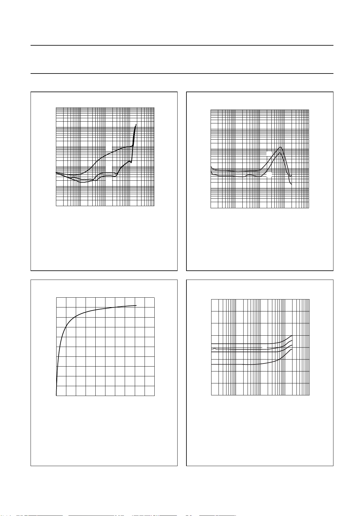
2 × 8 Ω SE; VP= ±15 V.
(1) 6 kHz.
(2) 1 kHz.
(3) 100 Hz.
(1)
(2)
(3)
−1
10
11010
MDB618
Po (W)
TDA8925
2
10
handbook, halfpage
THD + N
(%)
10
1
−1
10
−2
10
−3
2
10
10 10
2
(1)
(2)
3
10
2 × 8 Ω SE; VP= ±15 V.
(1) Po=10W.
(2) Po=1W.
MDB620
4
10
fi (Hz)
5
10
Fig.9 THD + N as function of output power.
100
handbook, halfpage
η
(%)
80
60
40
20
0
020
2 × 8 Ω SE; VP= ±15 V;
= 1 kHz.
f
i
4 8 12 16
MDB622
Po (W)
Fig.10 THD + N as function of frequency.
handbook, halfpage
0
SVRR
(dB)
−20
−40
−60
−80
10 10
VP= ±15 V; V
ripple(p-p)
2
=2V.
(1) Both supply lines in phase.
(2) One supply line (VSS) rippled.
(3) One supply line (VDD) rippled.
(4) Both supply lines in antiphase.
MDB619
(1)
(2)
(3)
(4)
3
10
4
10
fi (Hz)
5
10
Fig.11 Efficiency as function of output power.
2004 May 06 17
Fig.12 SVRR as function of frequency.
Page 18
Philips Semiconductors Product specification
Power stage 2 x 15 to 25 W class-D
audio amplifier
100
handbook, halfpage
S/N
(dB)
80
60
40
20
0
−2
10
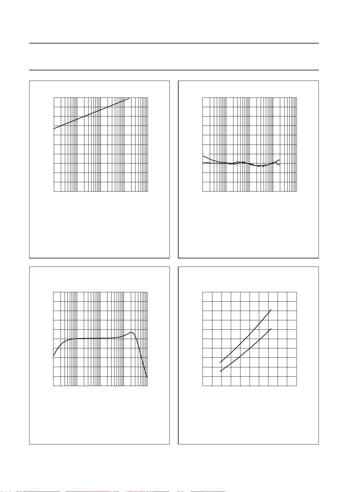
2 × 8 Ω SE; VP= ±15 V.
Fig.13 S/N as function of output power.
−1
10
11010
MDB621
2
Po (W)
handbook, halfpage
0
α
cs
(dB)
−20
−40
(1)
−60
(2)
−80
−100
10
2 × 8 Ω SE; VP= ±15 V.
(1) Po=1W.
(2) Po=10W.
10
2
3
10
Fig.14 Channel separation as function of
frequency.
TDA8925
MDB623
4
10
fi (Hz)
5
10
35
handbook, halfpage
G
(dB)
30
25
20
15
10
10
2 × 8 Ω SE; VP= ±15 V;
= 100 mV.
V
i
2
10
3
10
MDB624
4
10
fi (Hz)
5
10
Fig.15 Gain as function of frequency.
2004 May 06 18
25
handbook, halfpage
P
o
(W)
21
17
13
9
5
10
2 × 8 Ω SE; fi= 1 kHz.
(1) THD + N = 10 %.
(2) THD + N = 1 %.
(1)
(2)
12
14 16 18
MDB625
VP (V)
Fig.16 Output power as function of supply voltage.
20
Page 19
Philips Semiconductors Product specification
Power stage 2 x 15 to 25 W class-D
audio amplifier
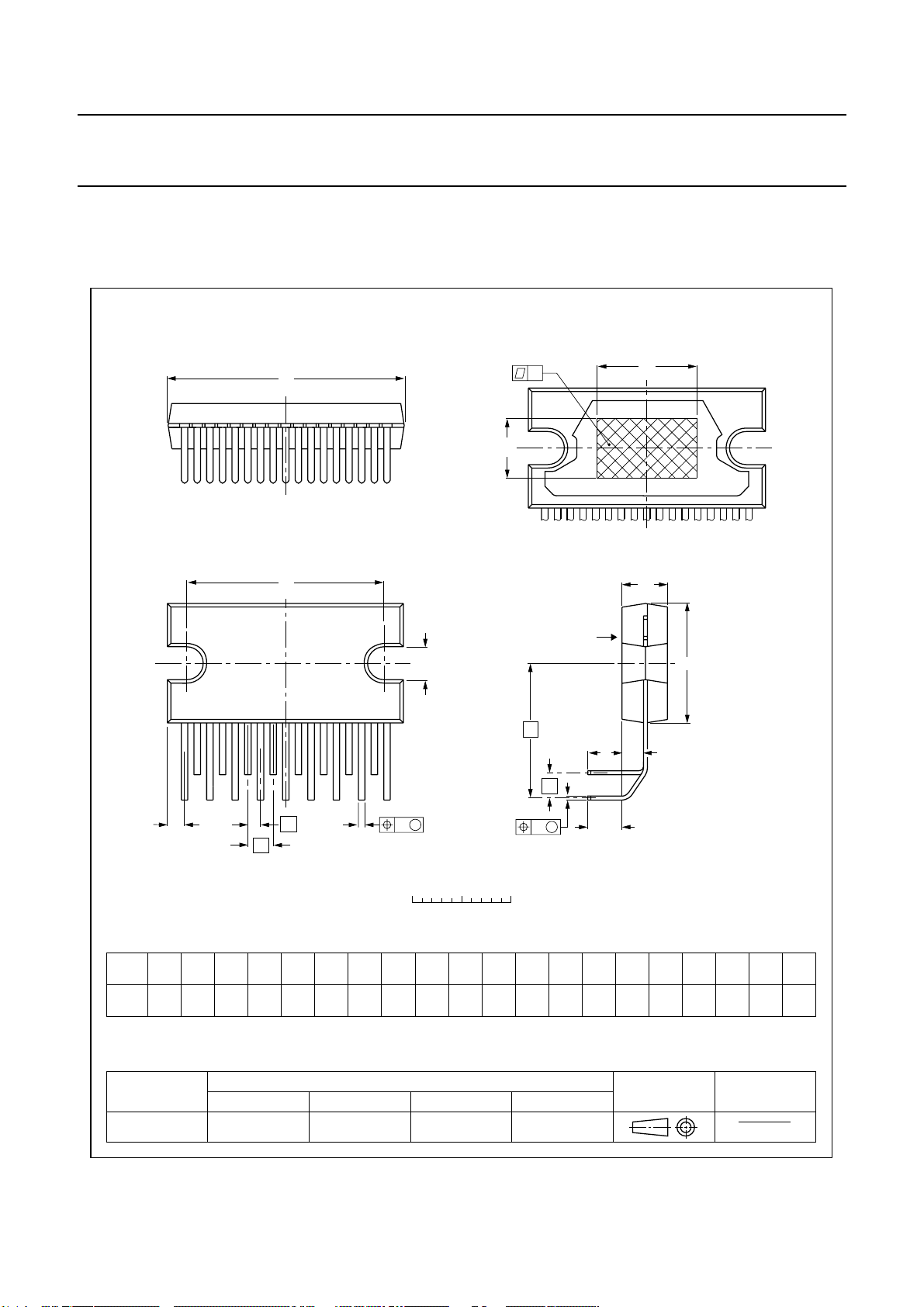
16 PACKAGE OUTLINES
RDBS17P: plastic rectangular-DIL-bent-SIL power package; 17 leads
(row spacing 2.54 mm)
non-concave
D
E
h
d
TDA8925
SOT577-2
D
x
view B: mounting base side
h
A
2
j
117
e
e
0.48
0.38
1
(1)
D
de LL
24.0
20.0
23.6
19.6
Z
DIMENSIONS (mm are the original dimensions)
UNIT A e1e
mm
Note
1. Plastic or metal protrusions of 0.25 mm maximum per side are not included.
A2bpcE
4.6
4.4
0.75
0.60
13.5
w
b
p
D
10 2.54
M
0 5 10 mm
(1)
h
12.2
11.8
scale
1.27 2.54
B
E
A
QL
c
e
2
M
v
E
2
h
6
3.4
3.1
3.75
3.15
L
1
x
0.03
(1)
Z
2.00
1.45
3.75
3.15
Qj
1
2.1
1.8
0.6
w
v
0.4
OUTLINE
VERSION
SOT577-2
IEC JEDEC JEITA
REFERENCES
2004 May 06 19
EUROPEAN
PROJECTION
ISSUE DATE
01-01-05
03-03-12
Page 20
Philips Semiconductors Product specification
Power stage 2 x 15 to 25 W class-D
audio amplifier
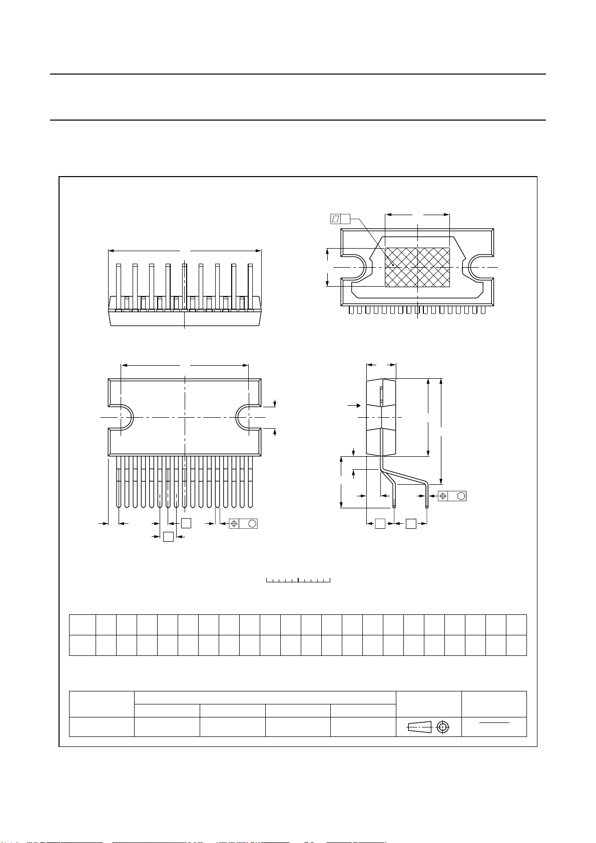
DBS17P: plastic DIL-bent-SIL power package; 17 leads (lead length 7.7 mm)
non-concave
x
D
E
h
view B: mounting base side
d
A
TDA8925
SOT243-3
D
h
2
j
117
e
0.48
0.38
1
e
(1)
deD
24.0
20.0
23.6
19.6
Z
DIMENSIONS (mm are the original dimensions)
UNIT A e
mm
Note
1. Plastic or metal protrusions of 0.25 mm maximum per side are not included.
A2bpcD
17.0
4.6
4.4
0.75
0.60
15.5
w
b
p
E
h
12.2
10 2.54
11.8
M
0 5 10 mm
scale
(1)
1
1.27
e
5.08
B
E
A
L
3
L
2.4
1.6
c
e
2
4.3
Q
m
3.4
3.1
LL3m
8.4
7.0
E
2
h
6
2.1
1.8
v
M
(1)
v
Qj
0.6
0.25w0.03
Z
x
2.00
1.45
OUTLINE
VERSION
SOT243-3
IEC JEDEC JEITA
REFERENCES
2004 May 06 20
EUROPEAN
PROJECTION
ISSUE DATE
99-12-17
03-03-12
Page 21

Philips Semiconductors Product specification
Power stage 2 x 15 to 25 W class-D
audio amplifier
17 SOLDERING
17.1 Introduction to soldering through-hole mount packages
This text gives a brief insight to wave, dip and manual
soldering.Amore in-depth account of soldering ICs can be
found in our
Packages”
Wave soldering is the preferred method for mounting of
through-hole mount IC packages on a printed-circuit
board.
17.2 Soldering by dipping or by solder wave
Driven by legislation and environmental forces the
worldwide use of lead-free solder pastes is increasing.
Typical dwell time of the leads in the wave ranges from
3 to 4 seconds at 250 °C or 265 °C, depending on solder
material applied, SnPb or Pb-free respectively.
“Data Handbook IC26; Integrated Circuit
(document order number 9398 652 90011).
TDA8925
Thetotalcontacttimeofsuccessivesolderwaves must not
exceed 5 seconds.
The device may be mounted up to the seating plane, but
the temperature of the plastic body must not exceed the
specified maximum storage temperature (T
printed-circuit board has been pre-heated, forced cooling
may be necessary immediately after soldering to keep the
temperature within the permissible limit.
17.3 Manual soldering
Apply the soldering iron (24 V or less) to the lead(s) of the
package, either below the seating plane or not more than
2 mm above it. If the temperature of the soldering iron bit
is less than 300 °C it may remain in contact for up to
10 seconds. If the bit temperature is between
300 and 400 °C, contact may be up to 5 seconds.
stg(max)
). If the
17.4 Suitability of through-hole mount IC packages for dipping and wave soldering methods
PACKAGE
DBS, DIP, HDIP, RDBS, SDIP, SIL suitable suitable
(2)
PMFP
Notes
1. For SDIP packages, the longitudinal axis must be parallel to the transport direction of the printed-circuit board.
2. For PMFP packages hot bar soldering or manual soldering is suitable.
− not suitable
DIPPING WAVE
SOLDERING METHOD
(1)
2004 May 06 21
Page 22

Philips Semiconductors Product specification
Power stage 2 x 15 to 25 W class-D
TDA8925
audio amplifier
18 DATA SHEET STATUS
LEVEL
I Objective data Development This data sheet contains data from the objective specification for product
II Preliminary data Qualification This data sheet contains data from the preliminary specification.
III Product data Production This data sheet contains data from the product specification. Philips
Notes
1. Please consult the most recently issued data sheet before initiating or completing a design.
2. The product status of the device(s) described in this data sheet may have changed since this data sheet was
published. The latest information is available on the Internet at URL http://www.semiconductors.philips.com.
3. For data sheets describing multiple type numbers, the highest-level product status determines the data sheet status.
DATA SHEET
STATUS
(1)
PRODUCT
STATUS
(2)(3)
development. Philips Semiconductors reserves the right to change the
specification in any manner without notice.
Supplementary data will be published at a later date. Philips
Semiconductors reserves the right to change the specification without
notice, in order to improve the design and supply the best possible
product.
Semiconductors reserves the right to make changes at any time in order
to improve the design, manufacturing and supply. Relevant changes will
be communicated via a Customer Product/Process Change Notification
(CPCN).
DEFINITION
19 DEFINITIONS Short-form specification The data in a short-form
specification is extracted from a full data sheet with the
same type number and title. For detailed information see
the relevant data sheet or data handbook.
Limiting values definition Limiting values given are in
accordance with the Absolute Maximum Rating System
(IEC 60134). Stress above one or more of the limiting
values may cause permanent damage to the device.
These are stress ratings only and operation of the device
attheseor at any other conditions above those given inthe
Characteristics sections of the specification is not implied.
Exposure to limiting values for extended periods may
affect device reliability.
Application information Applications that are
described herein for any of these products are for
illustrative purposes only. Philips Semiconductors make
norepresentationorwarrantythatsuchapplicationswillbe
suitable for the specified use without further testing or
modification.
20 DISCLAIMERS Life support applications These products are not
designed for use in life support appliances, devices, or
systems where malfunction of these products can
reasonably be expected toresult in personal injury. Philips
Semiconductorscustomersusingorsellingtheseproducts
for use in such applications do so at their own risk and
agree to fully indemnify Philips Semiconductors for any
damages resulting from such application.
Right to make changes Philips Semiconductors
reserves the right to make changes in the products including circuits, standard cells, and/or software described or contained herein in order to improve design
and/or performance. When the product is in full production
(status ‘Production’), relevant changes will be
communicated via a Customer Product/Process Change
Notification (CPCN). Philips Semiconductors assumes no
responsibility or liability for the use of any of these
products, conveys no licence or title under any patent,
copyright, or mask work right to these products, and
makes no representations or warranties that these
products are free from patent, copyright, or mask work
right infringement, unless otherwise specified.
2004 May 06 22
Page 23

Philips Semiconductors – a w orldwide compan y
Contact information
For additional information please visit http://www.semiconductors.philips.com. Fax: +31 40 27 24825
For sales offices addresses send e-mail to: [email protected].
© Koninklijke Philips Electronics N.V. 2004
All rights are reserved. Reproduction in whole or in part is prohibited without the prior written consent of the copyright owner.
The information presented in this document does not form part of any quotation or contract, is believed to be accurate and reliable and may be changed
without notice. No liability will be accepted by the publisher for any consequence of its use. Publication thereof does not convey nor imply any license
under patent- or other industrial or intellectual property rights.
Printed in The Netherlands R30/02/pp23 Date of release: 2004 May 06 Document order number: 9397 750 13042
SCA76
 Loading...