

Philips TDA8841H, TDA8842, TDA8841, TDA8840H, TDA8857H Datasheet
...
Tentative Device Specification
December 16, 1997
INTEGRATED CIRCUITS
Philips Semiconductors
TDA884X/5X-N2 series
I
2
C-bus controlled
PAL/NTSC/SECAM TV processors
DEVICE SPECIFICATION
Previous version: April 24, 1997

December 16, 1997 2
Philips Semiconductors Tentative Device Specification
I2C-bus controlled PAL/NTSC/SECAM
TV processors
TDA884X/5X-N2 series
FEATURES
The following features are available in all IC’s:
• Multi-standard vision IF circuit with an alignment-free
PLL demodulator without external components
• Alignment-free multi-standard FM sound demodulator
(4.5 MHz to 6.5 MHz)
• Audio switch
• Flexible source selection with CVBS switch and
Y(CVBS)/C input so that a comb filter can be applied
• Integrated chrominance trap circuit
• Integrated luminance delay line
• Asymmetrical peaking in the luminance channel with a
(defeatable) noise coring function
• Black stretching of non-standard CVBS or luminance
signals
• Integrated chroma band-pass filter with switchable
centre frequency
• Dynamic skin tone control circuit
• Blue stretch circuit which offsets colours near white
towards blue
• RGB control circuit with “Continuous Cathode
Calibration” and white point adjustment
• Possibility to insert a “blue back” option when no video
signal is available
• Horizontal synchronization with two control loops and
alignment-free horizontal oscillator
• Vertical count-down circuit
• Vertical driver optimised for DC-coupled vertical output
stages
• I2C-bus control of various functions
The detailed differences between the various IC’s are
given in the table on page 3.
GENERAL DESCRIPTION
The various versions of the TDA 884X/5X series are
I2C-bus controlled single chip TV processors which are
intended to be applied in PAL, NTSC, PAL/NTSC and
multi-standard television receivers. The N2 version is pin
and application compatible with the N1 version, however,
a new feature has been added which makes the N2 more
attractive. The IF PLL demodulator has been replaced by
an alignment-free IF PLL demodulator with internal VCO
(no tuned circuit required). The setting of the various
frequencies (33.4, 33.9, 38, 38.9, 45,75 and 58.75 MHz)
can be made via the I2C-bus.
Because of this difference the N2 version is compatible
with the N1, however, N1 devices cannot be used in an
optimised N2 application.
Functionally the IC series is split up is 3 categories, viz:
• Versions intended to be used in economy TV receivers
with all basic functions (envelope: S-DIP 56 and QFP
64)
• Versions with additional features like E-W geometry
control, H-V zoom function and YUV interface which are
intended for TV receivers with 110° picture tubes
(envelope: S-DIP 56)
• Versions which have in addition a second RGB input
with saturation control and a second CVBS output
(envelope: QFP 64)
The various type numbers are given in the table below.
SURVEY OF IC TYPES
ENVELOPE S-DIP 56 QFP 64
TV receiver category Economy Mid/High end Economy Mid/High end
PAL only TDA 8840 TDA 8840H
PAL/NTSC TDA 8841 TDA 8843 TDA 8841H
PAL/SECAM/NTSC TDA 8842 TDA 8844 TDA 8842H TDA 8854H
NTSC only TDA 8846/46A TDA 8847 TDA 8857H

December 16, 1997 3
Philips Semiconductors Tentative Device Specification
I2C-bus controlled PAL/NTSC/SECAM TV
processors
TDA884X/5X-N2 series
FUNCTIONAL DIFFERENCES BETWEEN THE VARIOUS IC VERSIONS
IC VERSION (TDA) 8840 8841 8842 8846 8846A 8843 8844 8847 8854H 8857H
Automatic Volume Limiting X X X X X
PAL decoder X X X X X X
SECAM decoder X X X
NTSC decoder X X X X X X X X X
Colour matrix PAL/NTSC(Japan) X X X X X
Colour matrix NTSC Japan/USA X X X X
YUV interface X X X X X X X
Base-band delay line for P AL and
SECAM or chroma comb filter for
NTSC
XXX XXX X
Adjustable luminance delay time X X X X X
Horizontal geometry X X X X X
Horizontal and vertical zoom X X X X X
Vertical scroll X X X X X
2nd CVBS output XX

December 16, 1997 4
Philips Semiconductors Tentative Device Specification
I2C-bus controlled PAL/NTSC/SECAM TV
processors
TDA884X/5X-N2 series
QUICK REFERENCE DATA
SYMBOL PARAMETER MIN. TYP. MAX. UNIT
Supply
V
P
supply voltage − 8.0 − V
I
P
supply current − 110 − mA
Input voltages
V
iVIFrms)
video IF amplifier sensitivity (RMS value) − 35 −µV
Vi
SIF(rms)
sound IF amplifier sensitivity (RMS value) − 1.0 − mV
V
iAUDIO(rms)
external audio input (RMS value) − 350 − mV
V
iCVBS(p-p)
external CVBS/Y input (peak-to-peak value) − 1.0 − V
V
iCHROMA(p-p)
external chroma input voltage (burst amplitude)
(peak-to-peak value)
− 0.3 − V
V
iRGB(p-p)
RGB inputs (peak-to-peak value) − 0.7 − V
Output signals
V
oCVBS(p-p)
demodulated CVBS output (peak-to-peak value) − 2.2 − V
I
oTUNER
tuner AGC output current range 0 − 5mA
V
oVIDSW(p-p)
CVBS1/CVBS2 output voltage of video switch
(peak-to-peak value)
− 2.0/1.0 − V
V
oB-Y(p-p)
−(R−Y) output/input voltage (peak-to-peak value) − 1.05 − V
V
oR-Y(p-p)
−(B−Y) output/input voltage (peak-to-peak value) − 1.33 − V
V
oY(p-p)
Y output/input voltage (peak-to-peak value) − 1.4 − V
V
oRGB(p-p)
RGB output signal amplitudes (peak-to-peak value) − 2.0 − V
I
oHOR
horizontal output current 10 −−mA
I
oVERT
vertical output current (peak-to-peak value) − 1 − mA
I
oEW
EW drive output current 1.2 −−mA
December 16, 1997 5
Philips Semiconductors Tentative Device Specification
I2C-bus controlled PAL/NTSC/SECAM TV
processors
TDA884X/5X-N2 series
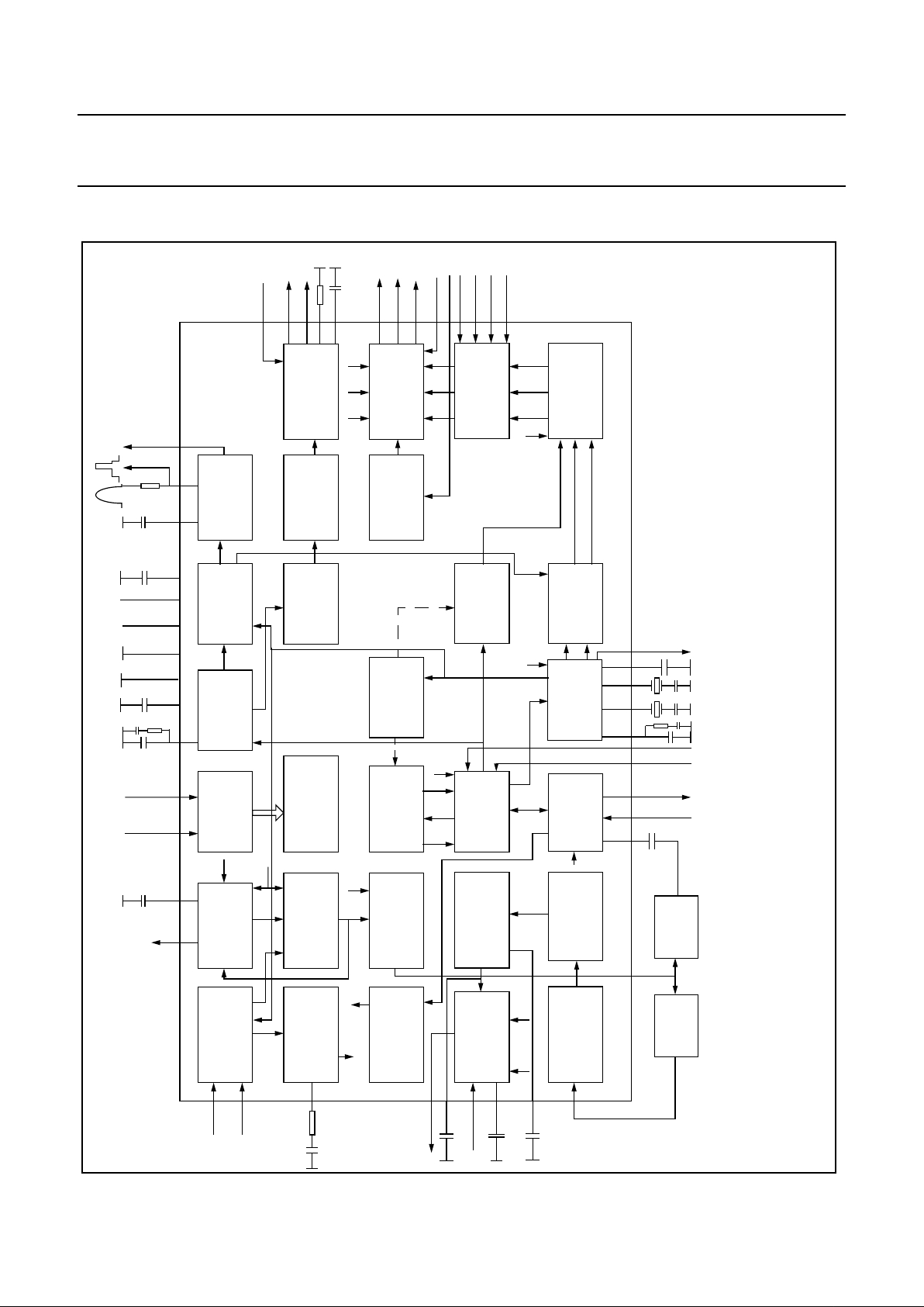
BLOCK DIAGRAMS
VIF AMPLIFIER
+ PLL DEMOD
AGC FOR IF
+ TUNER
I
2
C-BUS
TRANSCEIVER
SYNC SEP.
+ 1st LOOP
+ CONTROL
2nd LOOP
HOR.OUT
VCO
AFC
VIDEO
AMPLIFIER
CONTROL DAC’s
VERT. SYNC
SEPARATOR
H/V DIVIDER
VERTICAL
GEOMETRY
VIDEO IDENT VIDEO MUTE
CHROMA TRAP
+ BANDPASS
FILTER
TUNING
CONTINUOUS
CATHODE
CALIBRATION
RGB CONTROL
BLUE STRETCH
OUTPUT
SWITCH +
VOLUME
PRE-AMP.
+ MUTE
CVBS-Y/C
SWITCH
LUMA DELAY
PEAKING
CORING
BLACK STRETCH
RGB MATRIX
RGB-1 INPUT
LIMITER
PLL DEMOD.
CVBS SWITCH
PAL/NTSC
SECAM
DECODER
BASE-BAND
DELAY LINE
CD MATRIX
SAT. CONTROL
SKIN TINT
SOUND
BANDPASS
SOUND
TRAP
TUNER
SCL
SDA +8V
H-DRIVE
EHT
V-DRIVE
WHITE P BRI CONTR
RGB
BEAM CURR
BLACK CURR
R1
G1
B1
BL1
REF
REF
F
SC
CVBS IN
CVBS1 OUT
Chr
CVBS/Y
IF-IN
POL
AFC
IDENT
SW
SW
MUTE
TOP
AUDIO OUT
54 53 7 8 43 39 14
44
12 37 9 42 41 40
50
464752
51
212019
22
18
232425
26
33
16
343536
11
10
3817136
1
56
2
55
15
5
49
48
45
AUDIO IN
SAT
HUE
VOL SW
AVL +
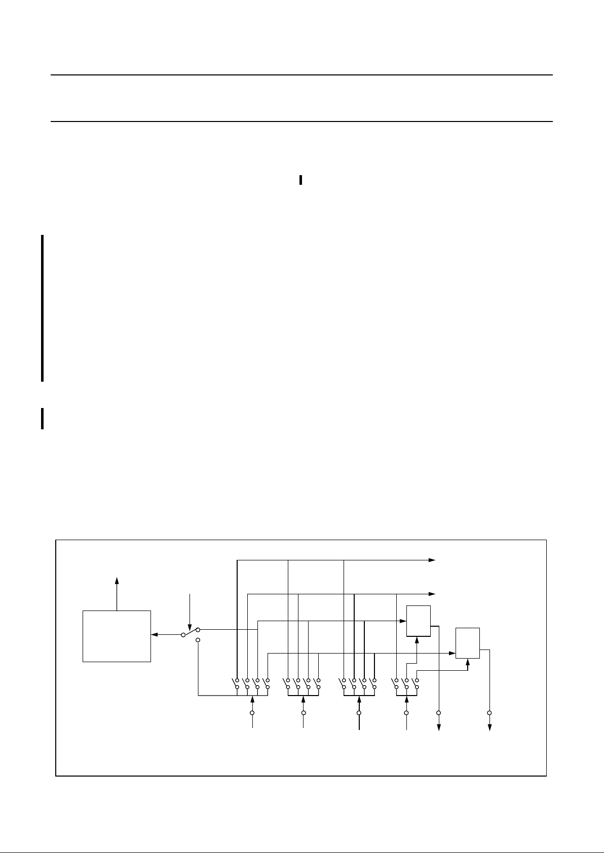
Fig.1 BLOCK DIAGRAM “ECONOMY VERSIONS” (S-DIP 56 ENVELOPE)
+CALIBRATION
December 16, 1997 6
Philips Semiconductors Tentative Device Specification
I2C-bus controlled PAL/NTSC/SECAM TV
processors
TDA884X/5X-N2 series
VIF AMPLIFIER
+ PLL DEMOD
AGC FOR IF
+ TUNER
I
2
C-BUS
TRANSCEIVER
SYNC SEP.
+ 1st LOOP
+ CONTROL
2nd LOOP
HOR.OUT
EW-GEOMETRY
VCO
AFC
VIDEO
AMPLIFIER
CONTROL DAC’s
VERT. SYNC
SEPARATOR
H/V DIVIDER
VERTICAL
GEOMETRY
VIDEO IDENT VIDEO MUTE
CHROMA TRAP
+ BANDPASS
FILTER
TUNING
CONTINUOUS
CATHODE
CALIBRATION
RGB CONTROL
BLUE STRETCH
OUTPUT
SWITCH +
VOLUME
PRE-AMP.
+ MUTE
CVBS-Y/C
SWITCH
LUMA DELAY
PEAKING
CORING
BLACK STRETCH
RGB MATRIX
RGB-1 INPUT
LIMITER
PLL DEMOD.
CVBS SWITCH
PAL/NTSC
SECAM
DECODER
BASE-BAND
DELAY LINE
CD MATRIX
SAT. CONTROL
SKIN TINT
SOUND
BANDPASS
SOUND
TRAP
TUNER
SCL
SDA +8V
H-DRIVE
EW
EHT
V-DRIVE
WHITE P BRI CONTR
RGB
BEAM CURR
BLACK CURR
R1
G1
B1
BL1
REF
REF
F
SC
CVBS IN
CVBS1 OUT
Chr
CVBS/Y
IF-IN
POL
AFC
IDENT
SW
SW
MUTE
TOP
AUDIO OUT
54 53 7 8 43 39 14
44
12 37 9 42 41 40
45
50
464752
51
212019
22
18
232425
26
33
16
343536
11
10
3817136
1
56
2
55
15
5
49
48
AUDIO IN
SAT
HUE
VOL SW
Fig.2 BLOCK DIAGRAM “MID/HIGH-END VERSIONS” (S-DIP 56 ENVELOPE)
+CALIBRATION
VU
Y
32 31 27302928
December 16, 1997 7
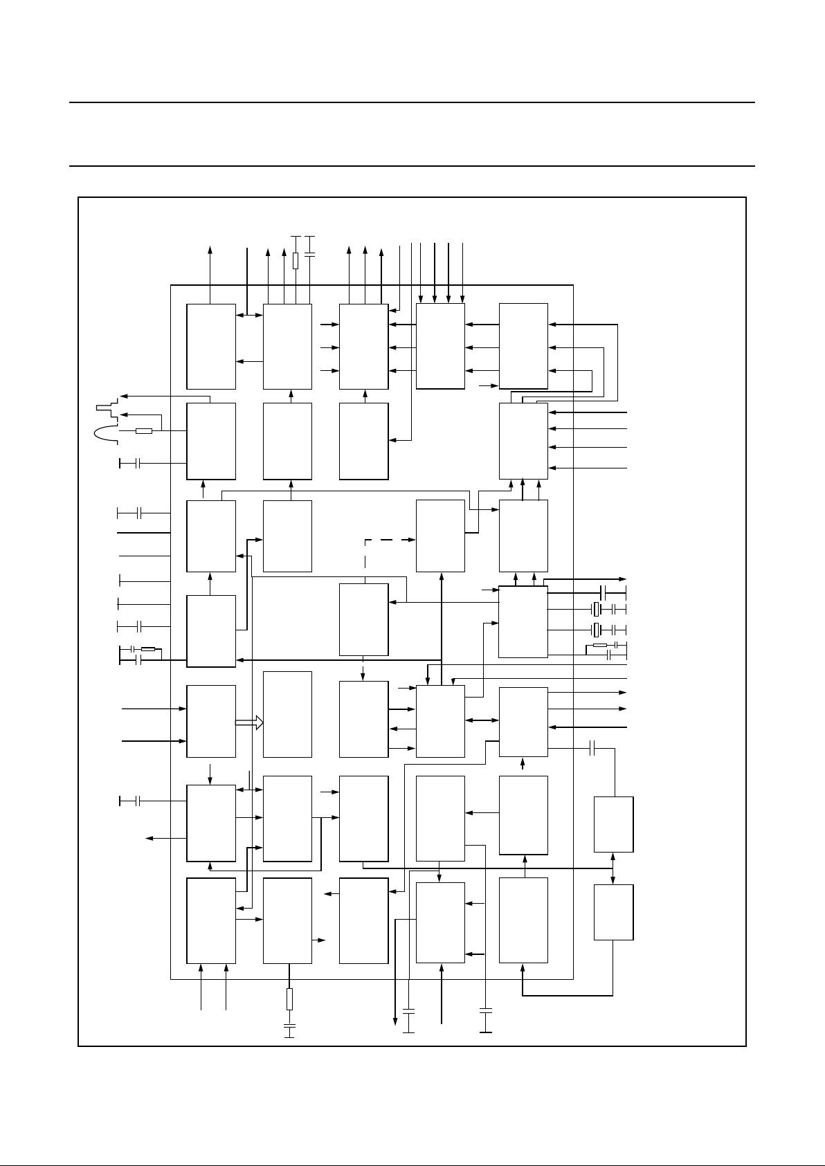
Philips Semiconductors Tentative Device Specification
I2C-bus controlled PAL/NTSC/SECAM TV
processors
TDA884X/5X-N2 series
VIF AMPLIFIER
+ PLL DEMOD
AGC FOR IF
+ TUNER
I
2
C-BUS
TRANSCEIVER
SYNC SEP.
+ 1st LOOP
+ CONTROL
2nd LOOP
HOR.OUT
EW-GEOMETRY
VCO
AFC
VIDEO
AMPLIFIER
CONTROL DAC’s
VERT. SYNC
SEPARATOR
H/V DIVIDER
VERTICAL
GEOMETRY
VIDEO IDENT VIDEO MUTE
CHROMA TRAP
+ BANDPASS
FILTER
TUNING
CONTINUOUS
CATHODE
CALIBRATION
RGB CONTROL
BLUE STRETCH
OUTPUT
SWITCH +
VOLUME
PRE-AMP.
+ MUTE
CVBS-Y/C
SWITCH
LUMA DELAY
PEAKING
CORING
BLACK STRETCH
RGB MATRIX
RGB-1 INPUT
LIMITER
PLL DEMOD.
CVBS SWITCH
PAL/NTSC
SECAM
DECODER
BASE-BAND
DELAY LINE
RGB-2 INPUT
RGB/YUV
MATRIX
CD MATRIX
SAT. CONTROL
SKIN TINT
SOUND
BANDPASS
SOUND
TRAP
TUNER
SCL
SDA +8V H-DRIVE
EW
EHT
V-DRIVE
WHITE P BRI CONTR
RGB
BEAM CURR
BLACK CURR
R1
G1
B1
BL1
V
UY
R2
G2 B2
BL2
REF
REF
F
SC
CVBS IN
CVBS1 OUT
CVBS2 OUT
Chr
CVBS/Y
IF-IN
POL
AFC
IDENT
SW
SW
MUTE
TOP
AUDIO OUT
76
17 18 59
28
25
60/61
22/23
53
19 58
57 56
62
3
63644
5
33
32313430353637
38
39474846
40
45
44434241
49
55
50
51522120
265429
24
16
10
9
11
8
27
15
2
1
AUDIO IN
SAT
HUE
VOL SW
Fig.3 BLOCK DIAGRAM “MID/HIGH-END VERSIONS” (QFP-64 ENVELOPE)
+CALIBRATION

December 16, 1997 8
Philips Semiconductors Tentative Device Specification
I2C-bus controlled PAL/NTSC/SECAM TV
processors
TDA884X/5X-N2 series
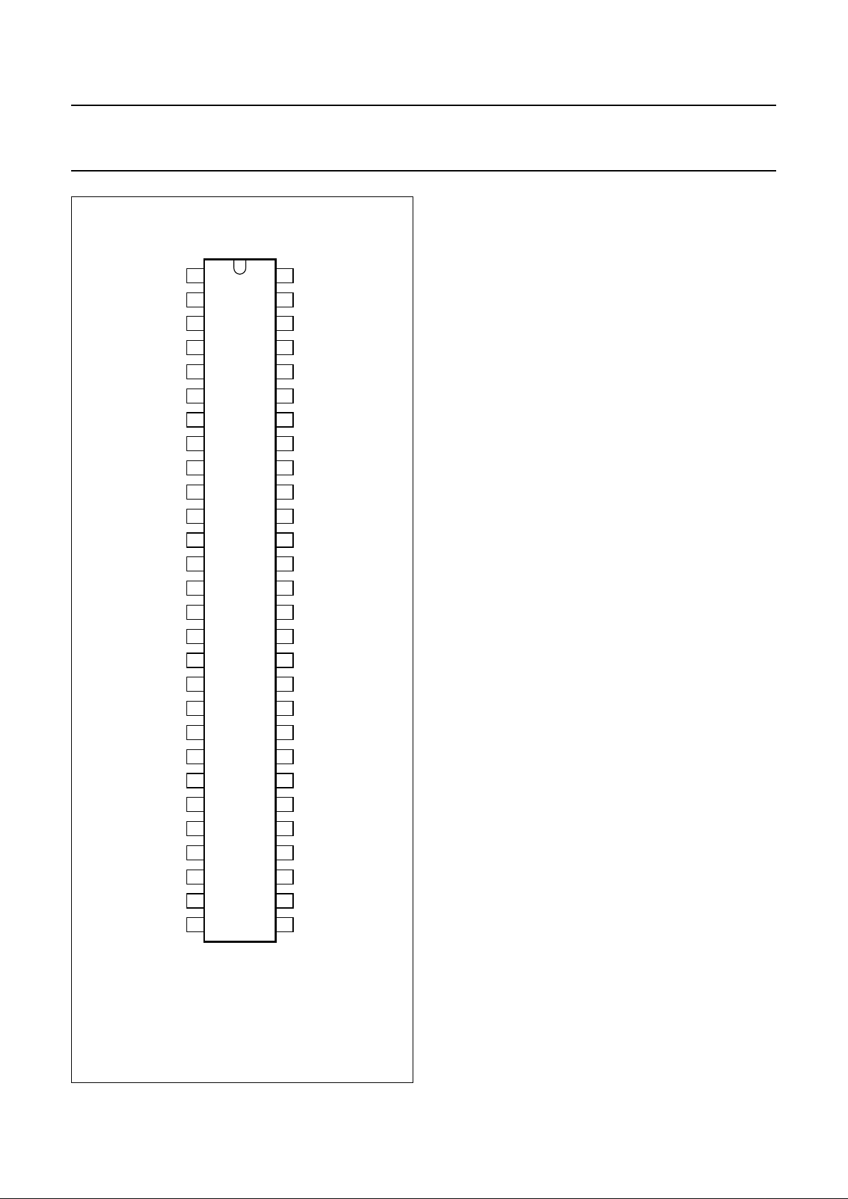
PINNING
SYMBOL
PIN
DESCRIPTION
SDIP56 QFP64
SNDIF 1 10 Sound IF input
AUDIOEXT 2 11 External audio input
NC 3 13 not connected
NC 4 14 not connected
PLLLF 5 15 IF-PLL loop filter
IFVO 6 16 IF video output
SCL 7 17 serial clock input
SDA 8 18 serial data input/output
DEC
BG
9 19 bandgap decoupling
CHROMA 10 20 chrominance input (S-VHS)
CVBS/Y 11 21 external CVBS/Y input
V
P1
12 22 main supply voltage 1 (+8 V)
CVBS
INT
13 24 internal CVBS input
GND1 14 25 ground 1
AUDIOOUT 15 27 audio output
SECPLL 16 28 SECAM PLL decoupling
CVBS
EXT
17 29 external CVBS input
BLKIN 18 30 black-current input
BO 19 31 blue output
GO 20 32 green output
RO 21 33 red output
BCLIN 22 34 beam current limiter input/V-guard input
RI 23 35 red input for insertion
GI 24 36 green input for insertion
BI 25 37 blue input for insertion
RGBIN 26 38 RGB insertion input
LUMIN 27 39 luminance input
LUMOUT 28 40 luminance output
BYO 29 45 (B−Y) signal output
RYO 30 46 (R−Y) signal output
BYI 31 47 (B−Y) signal input
RYI 32 48 (R−Y) signal input
REFO 33 49 subcarrier reference output
XTAL1 34 50 3.58 MHz crystal connection
XTAL2 35 51 4.43/3.58 MHz crystal connection
DET 36 52 loop filter phase detector
V
P2
37 53 2nd supply voltage 1(+8 V)
CVBS1O 38 54 CVBS-1 output

December 16, 1997 9
Philips Semiconductors Tentative Device Specification
I2C-bus controlled PAL/NTSC/SECAM TV
processors
TDA884X/5X-N2 series
The pin numbers mentioned in the rest of this document are referenced to the SDIP56 (SOT400) package.
In the TDA 8840/41/42/46/46A the following pins are different:
Pin 16 (SECAM PLL decoupling): Not connected in the TDA 8840/41/46/46A
Pin 27: Not connected in TDA 8840/41/42
Pin 28: Luminance output in TDA 8840/41/42
Pin 29-32 (U/V interface): Not available in TDA 8840/41/42
Pin 35 (4.43 MHz X-tal): Not connected in the TDA 8846/46A
Pin 45 (E-W drive output): AVL capacitor
In the TDA 8857H the pins 28 (SECAM PLL decoupling) and 51 (4.43 MHz X-tal) are not connected.
DECDIG 39 55 Decoupling digital supply
HOUT 40 56 horizontal output
FBISO 41 57 flyback input/sandcastle output
PH2LF 42 58 phase-2 filter
PH1LF 43 59 phase-1 filter
GND2 44 60 ground 2
EWD 45 62 east-west drive output
VDRB 46 63 vertical drive B output
VDRA 47 64 vertical drive A output
IFIN1 48 1 IF input 1
IFIN2 49 2 IF input 2
EHTO 50 3 EHT/overvoltage protection input
VSC 51 4 vertical sawtooth capacitor
I
ref
52 5 reference current input
DEC
AGC
53 6 AGC decoupling capacitor
AGCOUT 54 7 tuner AGC output
AUDEEM 55 8 Audio deemphasis
DECSDEM 56 9 Decoupling sound demodulator
n.c. − 12 not connected
VP3 − 23 Main supply voltage 2 (+8V)
CVBS2O − 26 CVBS-2 output
RI2 − 41 2nd R input
GI2. − 42 2nd G input
BI2 − 43 2nd B input
RGBIN2 − 44 2nd RGB insertion input
GND3 − 61 ground 3
SYMBOL
PIN
DESCRIPTION
SDIP56 QFP64
December 16, 1997 10
Philips Semiconductors Tentative Device Specification
I2C-bus controlled PAL/NTSC/SECAM TV
processors
TDA884X/5X-N2 series
Fig.4 Pin configuration (SDIP56).
handbook, halfpage
XXX
MXXxxx
1
2
3
4
5
6
7
8
9
10
11
12
13
14
15
16
17
18
19
20
21
22
23
24
25
26
27
28
56
55
54
53
52
51
50
49
48
47
46
45
44
43
42
41
40
39
38
37
36
35
34
33
32
31
30
29
TDA 884X
IFIN2
IFIN1
VDRA
VDRB
EWD
GND2
PH1LF
PH2LF
DECSDEM
AUDEEM
AGCOUT
DECAGC
IREF
VCS
EHTO
FBISO
HOUT
DECDIG
CVBS1O
VP2
DET
XTAL2
XTAL1
REFO
RYI
BYI
RYO
BYO
LUMOUT
LUMIN
RGBIN
BI
GI
RI
BCLIN
RO
GO
BO
BLKIN
CVBS
EXT
SECPLL
AUDOUT
GND1
CVBS
INT
VP1
CVBS/Y
CHROMA
DECBG
SDA
SCL
IFVO
PLLLF
NC
NC
AUDEXT
SNDIF

December 16, 1997 11
Philips Semiconductors Tentative Device Specification
I2C-bus controlled PAL/NTSC/SECAM TV
processors
TDA884X/5X-N2 series
Fig.5 Pin configuration (QFP64).
handbook, full pagewidth
XXX
MXXxxx
1
2
3
4
5
6
7
8
9
10
11
12
13
14
15
16
17
18
19
51
50
49
48
47
46
45
44
43
42
41
40
39
38
37
36
35
34
33
20
21
22
23
24
25
26
27
28
29
30
31
32
64
63
62
61
60
59
58
57
56
55
54
53
52
TDA 885X
GND3
VDRA
VRDB
EWD
GND2
PH1LF
PH2LF
FBISO
HOUT
DECDIG
CVBS1O
VP2
DET
XTAL2
XTAL1
REFO
RYI
BYI
RYO
BYO
RGB2IN
B2IN
G2IN
R2IN
LUMOUT
LUMIN
BI
RGBIN
GI
RI
BCLIN
RO
GO
BO
BLKIN
CVBS
EXT
SECPLL
AUDIOOUT
CVBS2O
GND1
CVBS
INT
VP3
VP1
CVBS/Y
CHROMA
IFIN1
DECSDEM
AUDEEM
AGCOUT
DECAGC
VCS
IREF
EHTO
IFIN2
SNDIF
AUDIOEXT
NC
NC
NC
PLLF
IFVO
SCL
SDA
DECBG
December 16, 1997 12
Philips Semiconductors Tentative Device Specification
I2C-bus controlled PAL/NTSC/SECAM TV
processors
TDA884X/5X-N2 series
FUNCTIONAL DESCRIPTION
Vision IF amplifier
The IF-amplifier contains 3 ac-coupled control stages with
a total gain control range which is higher then 66 dB. The
sensitivity of the circuit is comparable with that of modern
IF-IC’s.
The video signal is demodulated by means of an
alignment-free PLL carrier regenerator with an internal
VCO. This VCO is calibrated by means of a digital control
circuit which uses the X-tal frequency of the colour
decoder as a reference. The frequency setting for the
various standards (33.4, 33.9, 38, 38.9, 45.75 and 58.75
MHz) is realised via the I
2
C-bus. To get a good
performance for phase modulated carrier signals the
control speed of the PLL can be increased by means of the
FFI bit.
The AFC output is generated by the digital control circuit of
the IF-PLL demodulator and can be read via the I2C-bus.
For fast search tuning systems the window of the AFC can
be increased with a factor 3. The setting is realised with the
AFW bit. The AFC data is valid only when the horizontal
PLL is in lock (SL = 1)
Depending on the type the AGC-detector operates on
top-sync level (single standard versions) or on top sync
and top white- level (multi standard versions). The
demodulation polarity is switched via the I2C-bus. The
AGC detector time-constant capacitor is connected
externally. This mainly because of the flexibility of the
application. The time-constant of the AGC system during
positive modulation is rather long to avoid visible variations
of the signal amplitude. To improve the speed of the AGC
system a circuit has been included which detects whether
the AGC detector is activated every frame period. When
during 3 field periods no action is detected the speed of the
system is increased. For signals without peak white
information the system switches automatically to a gated
black level AGC. Because a black level clamp pulse is
required for this way of operation the circuit will only switch
to black level AGC in the internal mode.
The circuits contain a video identification circuit which is
independent of the synchronisation circuit. Therefore
search tuning is possible when the display section of the
receiver is used as a monitor. However, this ident circuit
cannot be made as sensitive as the slower sync ident
circuit (SL) and we recommend to use both ident outputs
to obtain a reliable search system. The ident output is
supplied to the tuning system via the I2C-bus.
The input of the identification circuit is connected to pin 13
(S-DIP 56 devices), the “internal” CVBS input (see Fig.6).
This has the advantage that the ident circuit can also be
made operative when a scrambled signal is received
(descrambler connected between pin 6 (IF video output)
and pin 13). A second advantage is that the ident circuit
can be used when the IF amplifier is not used (e.g. with
built-in satellite tuners).
The video ident circuit can also be used to identify the
selected CBVS or Y/C signal. The switching between the
2 modes can be realised with the VIM bit.
TO LUMA/SYNC PROCESSING
TO CHROMA PROCESSING
+
+
(26)
CVBS-2
38(54)
OUT
CVBS-1
OUT
10(20)
C
11(21)
Y/CVBS-3
17(29)
CVBS-EXT
13(24)
CVBS-INT
VIM
VIDEO IDENT
IDENT
Fig.6 CVBS switch and interfacing of video ident

December 16, 1997 13
Philips Semiconductors Tentative Device Specification
I2C-bus controlled PAL/NTSC/SECAM TV
processors
TDA884X/5X-N2 series
Video switches
The circuits have two CVBS inputs (internal and external
CVBS) and a Y/C input. When the Y/C input is not required
the Y input can be used as third CVBS input. The switch
configuration is given in Fig.6. The selection of the various
sources is made via the I2C-bus.
For the TDA 884X devices the video switch configuration
is identical to the switch of the TDA 8374/75 series. So the
circuit has one CVBS output (amplitude of 2 V
P-P
for the
TDA 884X series) and the I2C-bus control is similar to that
of the TDA 8374/75. For the TDA 885X IC’s the video
switch circuit has a second output (amplitude of 1 V
P-P
)
which can be set independently of the position of the first
output. The input signal for the decoder is also available on
the CVBS1-output.
Therefore this signal can be used to drive the Teletext
decoder. If S-VHS is selected for one of the outputs the
luminance and chrominance signals are added so that a
CVBS signal is obtained again.
Sound circuit
The sound bandpass and trap filters have to be connected
externally. The filtered intercarrier signal is fed to a limiter
circuit and is demodulated by means of a PLL
demodulator. This PLL circuit tunes itself automatically to
the incoming carrier signal so that no adjustment is
required.
The volume is controlled via the I2C-bus. The deemphasis
capacitor has to be connected externally. The
non-controlled audio signal can be obtained from this pin
(via a buffer stage).
The FM demodulator can be muted via the I2C-bus. This
function can be used to switch-off the sound during a
channel change so that high output peaks are prevented.
The TDA 8840/41/42/46 contain an Automatic Volume
Levelling (AVL) circuit which automatically stabilises the
audio output signal to a certain level which can be set by
the viewer by means of the volume control. This function
prevents big audio output fluctuations due to variations of
the modulation depth of the transmitter. The AVL function
can be activated via the I2C-bus.
Synchronisation circuit
The sync separator is preceded by a controlled amplifier
which adjusts the sync pulse amplitude to a fixed level.
These pulses are fed to the slicing stage which is operating
at 50% of the amplitude. The separated sync pulses are
fed to the first phase detector and to the coincidence
detector. This coincidence detector is used to detect
whether the line oscillator is synchronised and can also be
used for transmitter identification. This circuit can be made
less sensitive by means of the STM bit. This mode can be
used during search tuning to avoid that the tuning system
will stop at very weak input signals. The first PLL has a
very high statical steepness so that the phase of the
picture is independent of the line frequency.
The horizontal output signal is generated by means of an
oscillator which is running at twice the line frequency. Its
frequency is divided by 2 to lock the first control loop to the
incoming signal. The time-constant of the loop can be
forced by the I2C-bus (fast or slow). If required the IC can
select the time-constant depending on the noise content of
the incoming video signal.
The free-running frequency of the oscillator is determined
by a digital control circuit which is locked to the reference
signal of the colour decoder. When the IC is switched-on
the horizontal output signal is suppressed and the
oscillator is calibrated as soon as all sub-address bytes
have been sent. When the frequency of the oscillator is
correct the horizontal drive signal is switched-on. To obtain
a smooth switching-on and switching-off behaviour of the
horizontal output stage the horizontal output frequency is
doubled during switch-on and switch-off (slow start/stop).
During that time the duty cycle of the output pulse has such
a value that maximum safety is obtained for the output
stage.
To protect the horizontal output transistor the horizontal
drive is immediately switched off when a power-on-reset is
detected. The drive signal is switched-on again when the
normal switch-on procedure is followed, i.e. all
sub-address bytes must be sent and after calibration the
horizontal drive signal will be released again via the slow
start procedure. When the coincidence detector indicates
an out-of-lock situation the calibration procedure is
repeated. The circuit has a second control loop to generate
the drive pulses for the horizontal driver stage. The
horizontal output is gated with the flyback pulse so that the
horizontal output transistor cannot be switched-on during
the flyback time.
Via the I2C-bus adjustments can be made of the horizontal
and vertical geometry. The vertical sawtooth generator
drives the vertical output drive circuit which has a
differential output current. For the E-W drive a single
ended current output is available. A special feature is the
zoom function for both the horizontal and vertical
deflection and the vertical scroll function which are
available in some versions. When the horizontal scan is
reduced to display 4:3 pictures on a 16:9 picture tube an
accurate video blanking can be switched on to obtain well
defined edges on the screen.

December 16, 1997 14
Philips Semiconductors Tentative Device Specification
I2C-bus controlled PAL/NTSC/SECAM TV
processors
TDA884X/5X-N2 series
Overvoltage conditions (X-ray protection) can be detected
via the EHT tracking pin. When an overvoltage condition is
detected the horizontal output drive signal will be
switched-off via the slow stop procedure but it is also
possible that the drive is not switched-off and that just a
protection indication is given in the I2C-bus output byte.
The choice is made via the input bit PRD. The IC’s have a
second protection input on theϕ2 filter capacitor pin. When
this input is activated the drive signal is switched-off
immediately and switched-on again via the slow start
procedure. For this reason this protection input can be
used as “flash protection”.
The drive pulses for the vertical sawtooth generator are
obtained from a vertical countdown circuit. This countdown
circuit has various windows depending on the incoming
signal (50 Hz or 60 Hz and standard or non standard). The
countdown circuit can be forced in various modes by
means of the I2C-bus. During the insertion of RGB signals
the maximum vertical frequency is increased to 72 Hz so
that the circuit can also synchronise on signals with a
higher vertical frequency like VGA. To obtain short
switching times of the countdown circuit during a channel
change the divider can be forced in the search window by
means of the NCIN bit. The vertical deflection can be set
in the de-interlace mode via the I2C bus.
To avoid damage of the picture tube when the vertical
deflection fails the guard output current of the TDA
8350/51 can be supplied to the beam current limiting input.
When a failure is detected the RGB-outputs are blanked
and a bit is set (NDF) in the status byte of the I2C-bus.
When no vertical deflection output stage is connected this
guard circuit will also blank the output signals. This can be
overruled by means of the EVG bit.
Chroma and luminance processing
The circuits contain a chroma bandpass and trap circuit.
The filters are realised by means of gyrator circuits and
they are automatically calibrated by comparing the tuning
frequency with the X-tal frequency of the decoder. The
luminance delay line and the delay for the peaking circuit
are also realised by means of gyrator circuits. The centre
frequency of the chroma bandpass filter is switchable via
the I2C-bus so that the performance can be optimised for
“front-end” signals and external CVBS signals. During
SECAM reception the centre frequency of the chroma trap
is reduced to get a better suppression of the SECAM
carrier frequencies. All IC’s have a black stretcher circuit
which corrects the black level for incoming video signals
which have a deviation between the black level and the
blanking level (back porch). The timeconstant for the black
stretcher is realised internally.
The resolution of the peaking control DAC has been
increased to 6 bits. All IC’s have a defeatable coring
function in the peaking circuit. Some of these IC’s have a
YUV interface (see table on page 2) so that picture
improvement IC’s like the TDA 9170 (Contrast
improvement), TDA 9177 (Sharpness improvement) and
TDA 4556/66 (CTI) can be applied. When the CTI IC’s are
applied it is possible to increase the gain of the luminance
channel by means of the GAI bit in subaddress 03 so that
the resulting RGB output signals are not affected.
Colour decoder
Depending on the IC type the colour decoder can decode
PAL, PAL/NTSC or PAL/NTSC/SECAM signals. The
PAL/NTSC decoder contains an alignment-free X-tal
oscillator, a killer circuit and two colour difference
demodulators. The 90° phase shift for the reference signal
is made internally.
The IC’s contain an Automatic Colour Limiting (ACL)
circuit which is switchable via the I2C-bus and which
prevents that oversaturation occurs when signals with a
high chroma-to-burst ratio are received. The ACL circuit is
designed such that it only reduces the chroma signal and
not the burst signal. This has the advantage that the colour
sensitivity is not affected by this function.
The SECAM decoder contains an auto-calibrating PLL
demodulator which has two references, viz: the 4.4 MHz
sub-carrier frequency which is obtained from the X-tal
oscillator which is used to tune the PLL to the desired
free-running frequency and the bandgap reference to
obtain the correct absolute value of the output signal. The
VCO of the PLL is calibrated during each vertical blanking
period, when the IC is in search or SECAM mode.
The frequency of the active X-tal is fed to the Fsc output
(pin 33) and can be used to tune an external comb filter
(e.g. the SAA 4961).
The base-band delay line (TDA 4665 function) is
integrated in the PAL/SECAM IC’s and in the NTSC IC
TDA 8846A. In the latter IC it improves the cross colour
performance (chroma comb filter). The demodulated
colour difference signals are internally supplied to the
delay line. The colour difference matrix switches
automatically between PAL/SECAM and NTSC, however,
it is also possible to fix the matrix in the PAL standard.
The “blue stretch” circuit is intended to shift colour near
“white” with sufficient contrast values towards more blue to
obtain a brighter impression of the picture.

December 16, 1997 15
Philips Semiconductors Tentative Device Specification
I2C-bus controlled PAL/NTSC/SECAM TV
processors
TDA884X/5X-N2 series
Which colour standard the IC’s can decode depends on
the external X-tals. The X-tal to be connected to pin 34
must have a frequency of 3.5 MHz (NTSC-M, PAL-M or
PAL-N) and pin 35 can handle X-tals with a frequency of
4.4 and 3.5 MHz. Because the X-tal frequency is used to
tune the line oscillator the value of the X-tal frequency
must be given to the IC via the I2C-bus. It is also possible
to use the IC in the so called “Tri-norma” mode for South
America. In that case one X-tal must be connected to pin
34 and the other 2 to pin 35. The switching between the 2
latter X-tals must be done externally. This has the
consequence that the search loop of the decoder must be
controlled by the µ-computer. To prevent calibration
problems of the horizontal oscillator the external switching
between the 2 X-tals should be carried out when the
oscillator is forced to pin 34. For a reliable calibration of the
horizontal oscillator it is very important that the X-tal
indication bits (XA and XB) are not corrupted. For this
reason the X-tal bits can be read in the output bytes so that
the software can check the I2C-bus transmission.
Under bad-signal conditions (e.g. VCR-playback in feature
mode), it may occur that the colour killer is activated
although the colour PLL is still in lock. When this killing
action is not wanted it is possible to overrule the colour
killer by forcing the colour decoder to the required standard
and to activate the FCO-bit (Forced Colour On) in the
control-5 subaddress.
The IC’s contain a so-called “Dynamic skin tone (flesh)
control” feature. This function is realised in the YUV
domain by detecting the colours near to the skin tone. The
correction angle can be controlled via the I2C-bus.
RGB output circuit and black-current stabilisation
The colour-difference signals are matrixed with the
luminance signal to obtain the RGB-signals. The TDA
884X devices have one (linear) RGB input. This RGB
signal can be controlled on contrast and brightness (like
TDA 8374/75). By means of the IE1 bit the insertion
blanking can be switched on or off. Via the IN1 bit it can be
read whether the insertion pin has a high level or not.
The TDA 885X IC’s have an additional RGB input. This
RGB signal can be controlled on contrast, saturation and
brightness. The insertion blanking of this input can be
switched-off by means of the IE2 bit. Via the IN2 bit it can
be read whether the insertion pin has a high level or not.
The output signal has an amplitude of about 2 volts
black-to-white at nominal input signals and nominal
settings of the controls. To increase the flexibility of the IC
it is possible to insert OSD and/or teletext signals directly
at the RGB outputs. This insertion mode is controlled via
the insertion input (pin 26 in the S-DIP 56- and pin 38 in the
QFP-64 envelope). This blanking action at the RGB
outputs has some delay which must be compensated
externally.
To obtain an accurate biasing of the picture tube a
“Continuous Cathode Calibration” circuit has been
developed. This function is realised by means of a 2-point
black level stabilisation circuit. By inserting 2 test levels for
each gun and comparing the resulting cathode currents
with 2 different reference currents the influence of the
picture tube parameters like the spread in cut-off voltage
can be eliminated. This 2-point stabilisation is based on
the principle that the ratio between the cathode currents is
coupled to the ratio between the drive voltages according
to:
The feedback loop makes the ratio between the cathode
currents Ik1 and Ik2 equal to the ratio between the
reference currents (which are internally fixed) by changing
the (black) level and the amplitude of the RGB output
signals via 2 converging loops. The system operates in
such a way that the black level of the drive signal is
controlled to the cut-off point of the gun so that a very good
grey scale tracking is obtained. The accuracy of the
adjustment of the black level is just dependent on the ratio
of internal currents and these can be made very accurately
in integrated circuits. An additional advantage of the
2-point measurement is that the control system makes the
absolute value of Ik1 and Ik2 identical to the internal
reference currents. Because this adjustment is obtained
by means of an adaption of the gain of the RGB control
stage this control stabilises the gain of the complete
channel (RGB output stage and cathode characteristic).
As a result variations in the gain figures during life will be
compensated by this 2-point loop.
I
k1
I
k2
------ -
V
dr1
V
dr2
-----------
γ
=
December 16, 1997 16
Philips Semiconductors Tentative Device Specification
I2C-bus controlled PAL/NTSC/SECAM TV
processors
TDA884X/5X-N2 series
An important property of the 2-point stabilisation is that the
off-set as well as the gain of the RGB path is adjusted by
the feedback loop. Hence the maximum drive voltage for
the cathode is fixed by the relation between the test
pulses, the reference current and the relative gain setting
of the 3 channels. This has the consequence that the drive
level of the CRT cannot be adjusted by adapting the gain
of the RGB output stage. Because different picture tubes
may require different drive levels the typical “cathode drive
level” amplitude can be adjusted by means of an I2C-bus
setting. Dependent on the chosen cathode drive level the
typical gain of the RGB output stages can be fixed taking
into account the drive capability of the RGB outputs (pins
19 to 21). More details about the design will be given in the
application report.
The measurement of the “high” and the “low” current of the
2- point stabilisation circuit is carried out in 2 consecutive
fields. The leakage current is measured in each field. The
maximum allowable leakage current is 100 µA
When the TV receiver is switched-on the RGB output
signals are blanked and the black current loop will try to set
the right picture tube bias levels. Via the AST bit a choice
can be made between automatic start-up or a start-up via
the µ-processor. In the automatic mode the RGB drive
signals are switched-on as soon as the black current loop
has been stabilised. In the other mode the BCF bit is set to
0 when the loop is stabilised. The RGB drive can than be
switched-on by setting the AST bit to 0. In the latter mode
some delay can be introduced between the setting of the
BCF bit and the switching of the AST bit so that switch-on
effects can be suppressed.
It is also possible to start-up the devices with a fixed
internal delay (as with the TDA 837X and the TDA884X/5X
N1). This mode is activated with the BCO bit.
The vertical blanking is adapted to the incoming CVBS
signal (50 Hz or 60 Hz). When the flyback time of the
vertical output stage is longer than the 60 Hz blanking time
the blanking can be increased to the same value as that of
the 50 Hz blanking. This can be set by means of the LBM
bit.
For an easy (manual) adjustment of the Vg2 control voltage
the VSD bit is available. When this bit is activated the black
current loop is switched-off, a fixed black level is inserted
at the RGB outputs and the vertical scan is switched-off so
that a horizontal line is displayed on the screen. This line
can be used as indicator for the Vg2 adjustment. Because
of the different requirements for the optimum cut-off
voltage of the picture tube the RGB output level is
adjustable when the VSD bit is activated. The control
range is 2.5 ± 0.7 V and can be controlled via the
brightness control DAC.
It is possible to insert a so called “blue back” back-ground
level when no video is available. This feature can be
activated via the BB bit in the control2 subaddress.
I
2
C-BUS SPECIFICATION
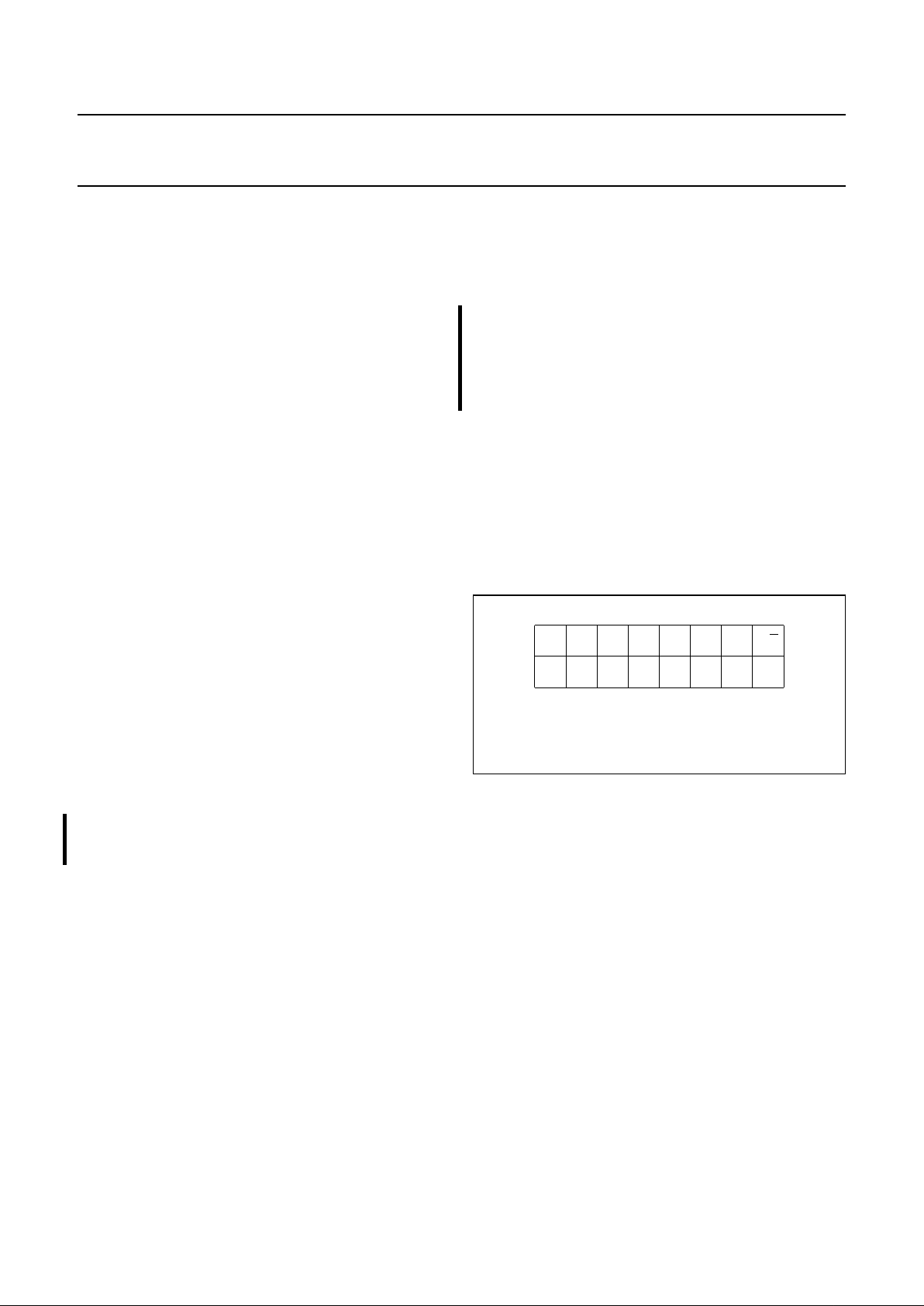
The slave address of the IC’s is given in Fig.7. The circuit
operates up to clock frequencies of 400 kHz.
Start-up procedure
Read the status bytes until POR =0 and send all
subaddress bytes. The horizontal output signal is
switched-on when the oscillator is calibrated.
Each time before the data in the IC is refreshed, the status
bytes must be read. If POR =1, the procedure mentioned
above must be carried out to restart the IC.
When this procedure is not followed the horizontal
frequency may be incorrect after power-up or after a
power dip.
handbook, halfpage
MLA743
A6 A5 A4 A3 A2 A1 A0
10001011/0
R/W
Fig.7 Slave address (8A).

December 16, 1997 17
Philips Semiconductors Tentative Device Specification
I2C-bus controlled PAL/NTSC/SECAM TV
processors
TDA884X/5X-N2 series
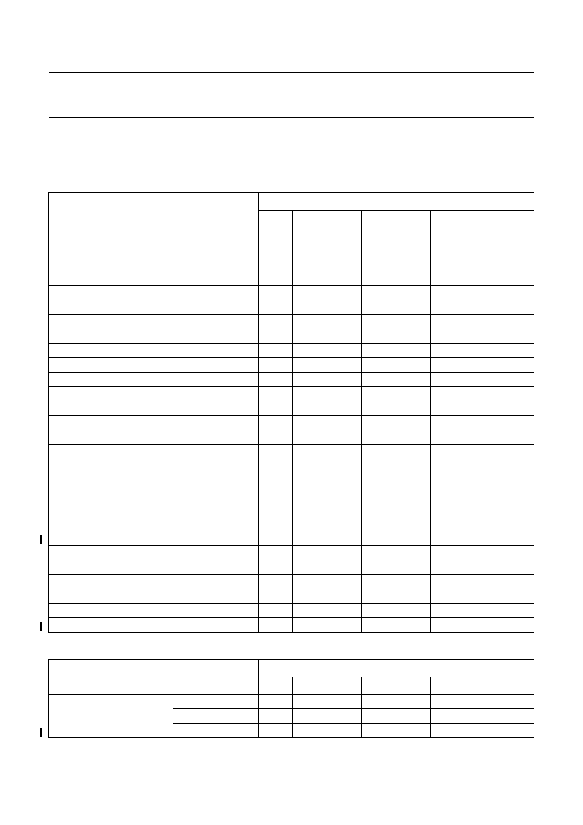
TDA 8840/41/42/46/46A:
Valid subaddresses: 00 to 1A (subaddresses 04 to 07 and 17 are not used), subaddress FE is reserved for test purposes.
Auto-increment mode available for subaddresses. The bit L’FA is only valid in the TDA 8842, the function of the colour
mode bits (CM0-CM2 and CD0-CD2) is dependent on the functional content of the IC.
Table 1 Input status bits.
Table 2 Output status bits.
FUNCTION
SUBADDRESS
(HEX)
DATA BYTE
D7 D6 D5 D4 D3 D2 D1 D0
Control 0 00 INA INB INC BCO FOA FOB XA XB
Control 1 01 FORF FORS DL STB POC CM2 CM1 CM0
Hue 02 AVL AKB A5 A4 A3 A2 A1 A0
Horizontal shift (HS) 03 VIM GAI A5 A4 A3 A2 A1 A0
Vertical slope (VS) 08 NCIN STM A5 A4 A3 A2 A1 A0
Vertical amplitude (VA) 09 VID LBM A5 A4 A3 A2 A1 A0
S-correction (SC) 0A 0 EVG A5 A4 A3 A2 A1 A0
Vertical shift (VSH) 0B SBL PRD A5 A4 A3 A2 A1 A0
White point R 0C 0 0 A5 A4 A3 A2 A1 A0
White point G 0D 0 0 A5 A4 A3 A2 A1 A0
White point B 0E MAT 0 A5 A4 A3 A2 A1 A0
Peaking 0F 0 0 A5 A4 A3 A2 A1 A0
Brightness 10 RBL COR A5 A4 A3 A2 A1 A0
Saturation 11 IE1 0 A5 A4 A3 A2 A1 A0
Contrast 12 AFW IFS A5 A4 A3 A2 A1 A0
AGC take-over 13 MOD VSW A5 A4 A3 A2 A1 A0
Volume control 14 SM FAV A5 A4 A3 A2 A1 A0
Adjustment IF-PLL 15 IFA IFB IFC 0 0 0 0 0
Control 2 18 OSO VSD CB BLS BKS 0 0 BB
Control 3 19 HOB BPS ACL CMB AST CL2 CL1 CL0
Control 4 1A 0 0 0 0 DS DSA FFI EBS
Control 5 1B 0 0 00000FCO
FUNCTION
SUBADDRESS
(HEX)
DATA BYTE
D7 D6 D5 D4 D3 D2 D1 D0
Output status bytes 00 POR FSI X SL XPR CD2 CD1 CD0
01 NDF IN1 X IFI AFA AFB SXA SXB
02 N2 X BCF IVW ID3 ID2 ID1 ID0
December 16, 1997 18
Philips Semiconductors Tentative Device Specification
I2C-bus controlled PAL/NTSC/SECAM TV
processors
TDA884X/5X-N2 series
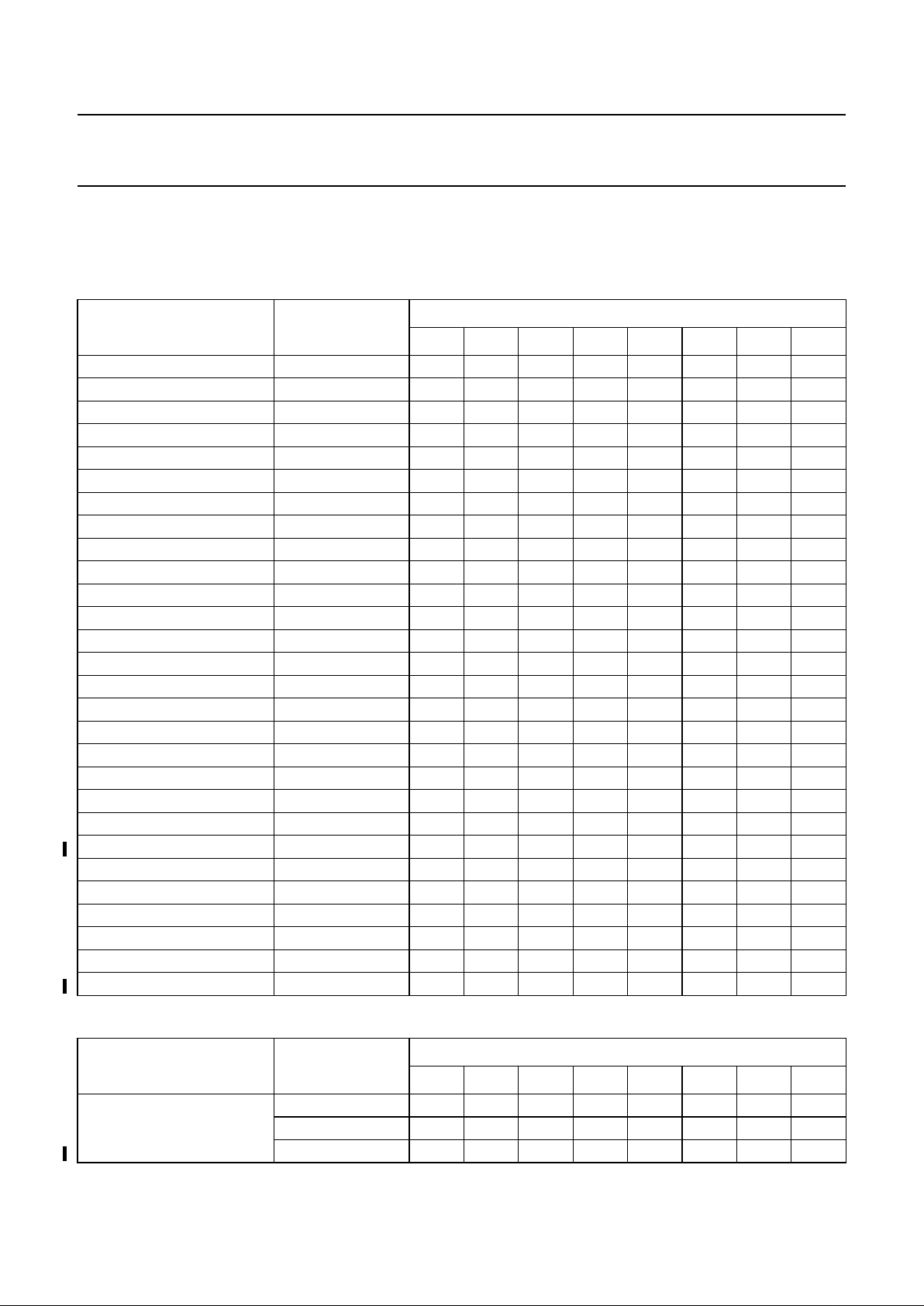
TDA 8843/44/47:
Valid subaddresses: 00 to 1A, subaddress FE is reserved for test purposes. Auto-increment mode available for
subaddresses. The bits L’FA, CM0-CM2 and CD0-CD2 are only available in the TDA 8843/44.
Table 3 Input status bits.
Table 4 Output status bits
FUNCTION
SUBADDRESS
(HEX)
DATA BYTE
D7 D6 D5 D4 D3 D2 D1 D0
Control 0 00 INA INB INC BCO FOA FOB XA XB
Control 1 01 FORF FORS DL STB POC CM2 CM1 CM0
Hue 02 HBL AKB A5 A4 A3 A2 A1 A0
Horizontal shift (HS) 03 VIM GAI A5 A4 A3 A2 A1 A0
EW width (EW) 04 0 0 A5 A4 A3 A2 A1 A0
EW parabola/width (PW) 05 0 0 A5 A4 A3 A2 A1 A0
EW corner parabola (CP) 06 0 0 A5 A4 A3 A2 A1 A0
EW trapezium (TC) 07 0 0 A5 A4 A3 A2 A1 A0
Vertical slope (VS) 08 NCIN STM A5 A4 A3 A2 A1 A0
Vertical amplitude (VA) 09 VID LBM A5 A4 A3 A2 A1 A0
S-correction (SC) 0A HCO EVG A5 A4 A3 A2 A1 A0
Vertical shift (VSH) 0B SBL PRD A5 A4 A3 A2 A1 A0
White point R 0C 0 0 A5 A4 A3 A2 A1 A0
White point G 0D 0 0 A5 A4 A3 A2 A1 A0
White point B 0E MAT 0 A5 A4 A3 A2 A1 A0
Peaking 0F 0 0 A5 A4 A3 A2 A1 A0
Brightness 10 RBL COR A5 A4 A3 A2 A1 A0
Saturation 11 IE1 0 A5 A4 A3 A2 A1 A0
Contrast 12 AFW IFS A5 A4 A3 A2 A1 A0
AGC take-over 13 MOD VSW A5 A4 A3 A2 A1 A0
Volume control 14 SM FAV A5 A4 A3 A2 A1 A0
Adjustment IF-PLL 15 IFA IFB IFC 0 0 0 0 0
Vertical zoom (VX) 16 0 0 A5 A4 A3 A2 A1 A0
Vertical scroll 17 0 0 A5 A4 A3 A2 A1 A0
Control 2 18 OSO VSD CB BLS BKS 0 0 BB
Control 3 19 HOB BPS ACL CMB AST CL2 CL1 CL0
Control 4 1A YD3 YD2 YD1 YD0 DS DSA FFI EBS
Control 5 1B 0 0 00000FCO
FUNCTION
SUBADDRESS
(HEX)
DATA BYTE
D7 D6 D5 D4 D3 D2 D1 D0
Output status bytes 00 POR FSI X SL XPR CD2 CD1 CD0
01 NDF IN1 X IFI AFA AFB SXA SXB
02 N2 X BCF IVW ID3 ID2 ID1 ID0
December 16, 1997 19
Philips Semiconductors Tentative Device Specification
I2C-bus controlled PAL/NTSC/SECAM TV
processors
TDA884X/5X-N2 series
TDA 8854/57:
Valid subaddresses: 00 to 1A, subaddress FE is reserved for test purposes. Auto-increment mode available for
subaddresses. The bits L’FA, CM0-CM2 and CD0-CD2 are only available in the TDA 8854.
Table 5 Input status bits.
Table 6 Output status bits
FUNCTION
SUBADDRESS
(HEX)
DATA BYTE
D7 D6 D5 D4 D3 D2 D1 D0
Control 0 00 INA INB INC BCO FOA FOB XA XB
Control 1 01 FORF FORS DL STB POC CM2 CM1 CM0
Hue 02 HBL AKB A5 A4 A3 A2 A1 A0
Horizontal shift (HS) 03 VIM GAI A5 A4 A3 A2 A1 A0
EW width (EW) 04 0 0 A5 A4 A3 A2 A1 A0
EW parabola/width (PW) 05 0 0 A5 A4 A3 A2 A1 A0
EW corner parabola (CP) 06 0 0 A5 A4 A3 A2 A1 A0
EW trapezium (TC) 07 0 0 A5 A4 A3 A2 A1 A0
Vertical slope (VS) 08 NCIN STM A5 A4 A3 A2 A1 A0
Vertical amplitude (VA) 09 VID LBM A5 A4 A3 A2 A1 A0
S-correction (SC) 0A HCO EVG A5 A4 A3 A2 A1 A0
Vertical shift (VSH) 0B SBL PRD A5 A4 A3 A2 A1 A0
White point R 0C 0 0 A5 A4 A3 A2 A1 A0
White point G 0D 0 0 A5 A4 A3 A2 A1 A0
White point B 0E MAT 0 A5 A4 A3 A2 A1 A0
Peaking 0F 0 0 A5 A4 A3 A2 A1 A0
Brightness 10 RBL COR A5 A4 A3 A2 A1 A0
Saturation 11 IE1 IE2 A5 A4 A3 A2 A1 A0
Contrast 12 AFW IFS A5 A4 A3 A2 A1 A0
AGC take-over 13 MOD VSW A5 A4 A3 A2 A1 A0
Volume control 14 SM FAV A5 A4 A3 A2 A1 A0
Adjustment IF-PLL 15 IFA IFB IFC 0 0 0 0 0
Vertical zoom (VX) 16 0 0 A5 A4 A3 A2 A1 A0
Vertical scroll 17 0 0 A5 A4 A3 A2 A1 A0
Control 2 18 OSO VSD CB BLS BKS CS1 CS0 BB
Control 3 19 HOB BPS ACL CMB AST CL2 CL1 CL0
Control 4 1A YD3 YD2 YD1 YD0 DS DSA FFI EBS
Control 5 1B 0 0 00000FCO
FUNCTION
SUBADDRESS
(HEX)
DATA BYTE
D7 D6 D5 D4 D3 D2 D1 D0
Output status bytes 00 POR FSI X SL XPR CD2 CD1 CD0
01 NDF IN1 IN2 IFI AFA AFB SXA SXB
02 N2 X BCF IVW ID3 ID2 ID1 ID0
December 16, 1997 20
Philips Semiconductors Tentative Device Specification
I2C-bus controlled PAL/NTSC/SECAM TV
processors
TDA884X/5X-N2 series
INPUT CONTROL BITS
Table 7 Source select
Note
1. These modes are intended for comb filter applications.
Table 8 Switch-on behaviour
Table 9 Phase 1 (ϕ1) time constant
Table 10 Crystal indication
Table 11 Forced field frequency
INA INB INC SELECTED SIGNALS
CVBS1
OUTPUT
0 0 0 Internal CVBS+ audio Int. CVBS
0 0 1 External CVBS+ audio Ext. CVBS
0 1 0 Y/C + ext. audio Y/C(Y+C)
0 1 1 CVBS3 + ext. audio CVBS3
1 0 0 Y/C + int audio, note 1 Int CVBS
1 1 0 Y/C + ext audio, note 1 Ext. CVBS
BCO STATUS
0 switch-on of picture without delay
1 switch-on of picture via internal delay
FOA FOB MODE
0 0 normal
0 1 slow
1 0 slow/fast
1 1 fast
XA XB CRYSTAL
0 0 two 3.6 MHz
0 1 one 3.6 MHz (pin 34)
1 0 one 4.4 MHz (pin 35)
1 1 3.6 MHz (pin 34) and 4.4 MHz
(pin 35)
FORF FORS FIELD FREQUENCY
0 0 auto (60 Hz when line not in sync)
0 1 60 Hz
1 0 keep last detected field frequency
1 1 auto (50 Hz when line not in sync)
Table 12 Interlace
Table 13 Stand-by
Table 14 Synchronization mode
Table 15 Colour decoder mode
Table 16 Auto. Volume Levelling (TDA 8840/1/2/6/6A)
Table 17 RGB blanking mode (TDA 8843/44/47/54/57)
Table 18 Black current stabilisation
DL STATUS
0 interlace
1 de-interlace
STB MODE
0 stand-by
1 normal
POC MODE
0 active
1 not active
CM2 CM1 CM0 DECODER MODE
0 0 0 not forced, own intelligence
0 0 1 forced X-tal pin 34 PAL/NTSC
0 1 0 forced X-tal pin 34 PAL
0 1 1 forced X-tal pin 34 NTSC
1 0 0 forced X-tal pin 35 PAL/NTSC
1 0 1 forced X-tal pin 35 PAL
1 1 0 forced X-tal pin 35 NTSC
1 1 1 Forced SECAM (X-tal pin 35)
AVL MODE
0 not active
1 active
HBL MODE
0 normal blanking (horizontal flyback)
1 wide blanking
AKB MODE
0 active
1 not active
December 16, 1997 21
Philips Semiconductors Tentative Device Specification
I2C-bus controlled PAL/NTSC/SECAM TV
processors
TDA884X/5X-N2 series
Table 19 Video ident mode
Table 20 Gain of luminance channel
Table 21 Vertical divider mode
Table 22 Search tuning mode
Table 23 Video ident mode
Table 24 Long blanking mode
Table 25 EHT tracking mode
Table 26 Enable vertical guard (RGB blanking)
VIM MODE
0 ident coupled to internal CVBS (pin 13)
1 ident coupled to selected CVBS
GAI MODE
0 normal gain (V27 = 1 VBL-WH)
1 high gain (V27 = 0.45 VP-P)
NCIN VERTICAL DIVIDER MODE
0 normal operation
1 switched to search window
STM MODE
0 normal operation
1 reduced sensitivity of video indent circuit
VID VIDEO IDENT MODE
0 ϕ1 loop switched on and off
1 not active
LBM BLANKING MODE
0 adapted to standard (50 or 60 Hz)
1 fixed in accordance with 50 Hz standard
HCO TRACKING MODE
0 EHT tracking only on vertical
1 EHT tracking on vertical and EW
EVG VERTICAL GUARD MODE
0 not active
1 active
Table 27 Service blanking
Table 28 Overvoltage input mode
Table 29 PAL-SECAM/NTSC matrix (TDA8841/2/3/4/54)
Table 30 NTSC matrix (TDA 8846/46A/47/57)
Table 31 RGB blanking
Table 32 Noise coring (peaking)
Table 33 Enable fast blanking RGB-1
Table 34 Enable fast blanking RGB-2 (TDA 885X)
SBL SERVICE BLANKING MODE
0off
1on
PRD OVERVOLTAGE MODE
0 detection mode
1 protection mode
MAT MATRIX POSITION
0 adapted to standard
1 PAL matrix
MAT MATRIX POSITION
0 Japanese matrix
1 USA matrix
RBL RGB BLANKING
0 not active
1 active
COR NOISE CORING
0off
1on
IE1 FAST BLANKING
0 not active
1 active
IE2 FAST BLANKING
0 not active
1 active
 Loading...