

Philips tda8822 DATASHEETS

INTEGRATED CIRCUITS
DATA SH EET
TDA8822
Universal I
2
C-bus programmable
RF modulator
Preliminary specification
File under Integrated Circuits, IC02
1997 Jan 08

Philips Semiconductors Preliminary specification
Universal I2C-bus programmable RF
modulator
FEATURES
• 5 V power supply
• Video amplifier with clamp and white clip circuits
• Programmable video modulation depth
• FM sound modulator (4.5, 5.5, 6.0 and 6.5 MHz)
• Programmable picture-to-sound ratio
• Programmable deviation of the sound subcarrier
• Input for modulated NICAM sound subcarrier or second
frequency modulated sound subcarrier
• Asymmetrical or symmetrical RF output buffer
• Symmetrical RF oscillator for UHF or VHF band
according to the application
• One I2C-bus programmable output port
• On-chip Phase-Locked Loop (PLL) frequency
synthesizer for the RF carrier
• On-chip PLL frequency synthesizer for the sound carrier
• On-chip power supply regulator
• On-chip I2C-bus and/or hardware controlled Test
Pattern Signal Generator (TPSG) with LED driver
• RF output switch-off during tuning.
APPLICATIONS
• Video recorders
• Cable converters
• Satellite receivers
• Set top boxes.
TDA8822
GENERAL DESCRIPTION
The TDA8822 is a programmable modulator which
generates an RF TV channel from a baseband video
signal and a baseband audio signal in the event of
negative video and FM sound standards (B/G, I, D/K, M
and N standards).
Two PLL frequency-synthesizers set the picture carrier
frequency and the sound subcarrier frequency to the
required frequencies. These PLL frequency-synthesizers
are programmed via the I
The I2C-bus controls these features:
• Video modulation depth
• Sound subcarrier modulation deviation
• Picture-to-sound ratio.
This makes the IC suitable for multistandard applications
without any adjustment into the application.
Additional features are provided like an input for the
NICAM or second FM carrier, a test pattern signal
generator with a LED driver and a general purpose
output port.
2
C-bus.
ORDERING INFORMATION
TYPE
NUMBER
TDA8822T SO24 plastic small outline package; 24 leads; body width 7.5 mm SOT137-1
TDA8822M SSOP24 plastic shrink small outline package; 24 leads; body width 5.3 mm SOT340-1
1997 Jan 08 2
NAME DESCRIPTION VERSION
PACKAGE

Philips Semiconductors Preliminary specification
Universal I2C-bus programmable RF
TDA8822
modulator
QUICK REFERENCE DATA
V
CCA=VCCD
PS setting = 1; video input signal = 500 mV (p-p) EBU colour bars; audio input signal = 45 mV (p-p); 1 kHz sine wave;
unless otherwise specified.
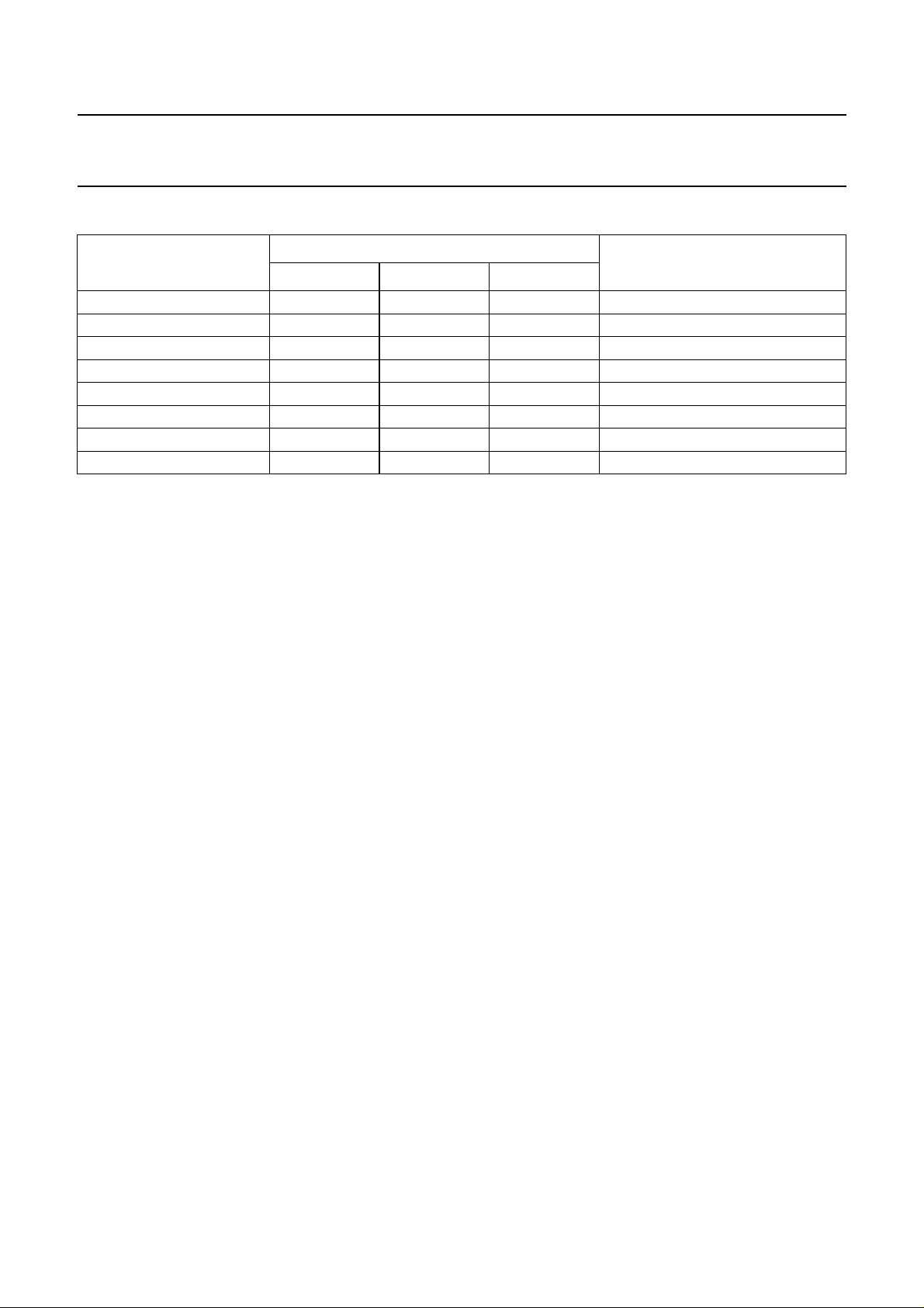
SYMBOL PARAMETER CONDITIONS MIN. TYP. MAX. UNIT
V
CCA
V
CCD
I
CC(tot)
m
d
P/S picture-to-sound ratio
V
RF
f
sc
∆f
sc
=5V; T
=25°C; in PAL B/G, PAL I, PAL D/K or NTSC; MD setting = 4; DEV setting = 2;
amb
analog supply voltage 4.5 5.0 5.5 V
digital supply voltage 4.5 5.0 5.5 V
total supply current − 60 72 mA
modulation depth adjustment
range
adjustment range
RF output voltage level
typical value for MD setting between
72.5 − 90.0 %
0 and 7
typical value for PS setting between
−18 −−11 dB
0 and 7
frequency between 45 and 860 MHz 77 80 83 dBµV
asymmetrical on a 75 Ω load
sound subcarrier frequency 4.5 − 6.5 MHz
sound subcarrier frequency
deviation range
for B/G, I, D/K, SC setting = 1, 2 or 3;
typical value for DEV setting between
20 − 45 kHz
0 and 7
for M, N, SC setting = 0; typical value
10 − 22.5 kHz
for DEV setting between 0 and 7
1997 Jan 08 3
Philips Semiconductors Preliminary specification
Universal I2C-bus programmable RF
modulator
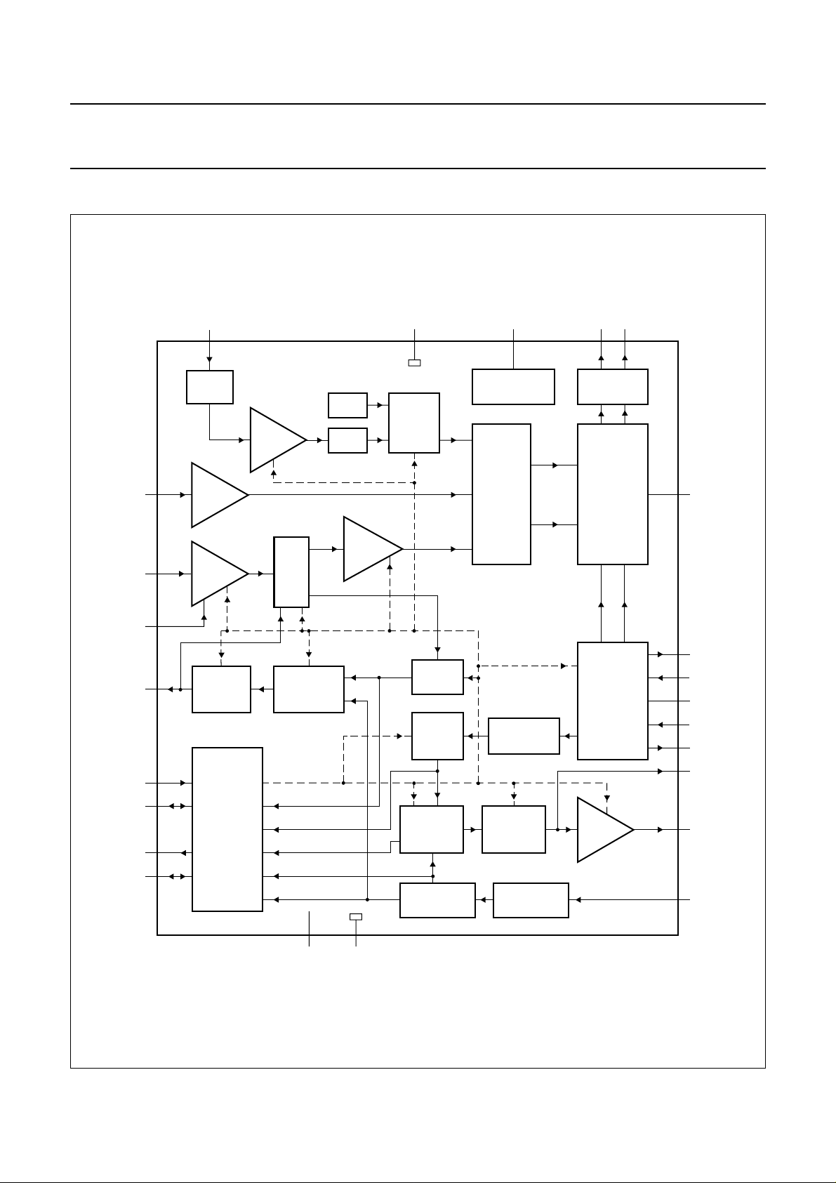
BLOCK DIAGRAM
handbook, full pagewidth
NICAM
VIDEO
24
CLAMP
TPSG
VIDEO
AMP.
MD setting
21
NICAM
AMP.
CLIP
AGND
23
SWITCH
TPSG
ON/OFF
V
CCA
1
VOLTAGE
REGULATOR
ADDER
RFA RFB
OUTPUT
BUFFER
MIXER
1819
TDA8822
20
RFGND
AUDIO
PREEMPH
ACP
SCL
SDA
P0
TPSG
SND-IF
22
AUDIO
AMP.
DEV
setting
3
test test
2
14
15
16
17
AUDIO
CHARGE
PUMP
2
I
C-BUS
RECEIVER
AND
LOGIC
VCO
AUDIO
PHASE
DETECTOR
I2C-bus control
f
div(audio)
f
div(video)
in-lock flag
f
ref(video)
f
ref(audio)
V
CCD
AMP.
setting
sound oscillator
ON/OFF
frequency
setting
11 13
DGND
PS
PROG.
DIVIDER
14 BITS
PROG.
DIVIDER
test test
VIDEO
PHASE
DETECTOR
REFERENCE
DIVIDER
frequency
setting
PRESCALER
DIVIDE-BY-8
CHARGE
TDA8822
RF oscillator
ON/OFF
VIDEO
PUMP
CRYSTAL
OSCILLATOR
RF
OSCILLATOR
test
LOOP
AMP.
10
12
MGE674
4
5
6
7
8
9
RFOSCA
RFOSCB
OGND
RFOSCC
RFOSCD
VCP
VVT
XTAL
Fig.1 Block diagram.
1997 Jan 08 4
Philips Semiconductors Preliminary specification
Universal I2C-bus programmable RF
modulator
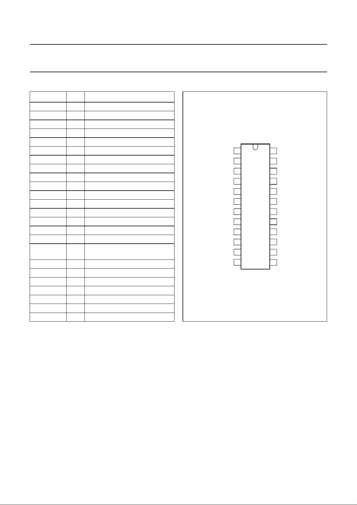
PINNING
SYMBOL PIN DESCRIPTION
V
CCA
ACP 2 audio charge pump output
PREEMPH 3 audio pre-emphasis network
RFOSCA 4 RF oscillator A (collector) output
RFOSCB 5 RF oscillator B (base) input
OGND 6 RF oscillator ground
RFOSCC 7 RF oscillator C (base) input
RFOSCD 8 RF oscillator D (collector) output
VVT 9 video tuning voltage output
VCP 10 video charge pump output
V
CCD
XTAL 12 crystal oscillator input
DGND 13 digital ground
SCL 14 serial clock (I
SDA 15 serial data (I
P0 16 general purpose output
TPSG 17 test pattern signal generator
RFB 18 RF output B
RFA 19 RF output A
RFGND 20 ground for the RF outputs
NICAM 21 NICAM input
AUDIO 22 audio input
AGND 23 analog ground
VIDEO 24 video input
1 analog power supply
11 digital power supply
2
C-bus) input
2
C-bus) input/output
input/output pin
handbook, halfpage
PREEMPH
RFOSCA
RFOSCB
RFOSCC
RFOSCD
V
1
CCA
ACP
2
3
4
5
OGND
6
TDA8822
7
8
VVT
9
VCP
10
V
11
CCD
XTAL
12
MGE673
Fig.2 Pin configuration.
TDA8822
VIDEO
24
AGND
23
AUDIO
22
NICAM
21
RFGND
20
19
RFA
RFB
18
17
TPSG
P0
16
SDA
15
SCL
14
DGND
13
1997 Jan 08 5
Philips Semiconductors Preliminary specification
Universal I2C-bus programmable RF
modulator
FUNCTIONAL DESCRIPTION
The TDA8822 is a programmable RF modulator which can
be divided into the following parts:
• Video part
• Audio part
• RF part.
Video part
The video part provides the following:
• The video part includes a clamping circuit which sets the
internal reference voltage to the bottom of the
synchronizing pulse. The modulation depth is adjusted
using 3 bits of the I
MD1 and MD0. These 3 bits make 8 different values for
the modulation depth possible (see Table 1).
• After the modulation depth is set, the signal is fed
through a clip control circuit that clips the video signal to
avoid that the modulation depth becomes higher than
100%.
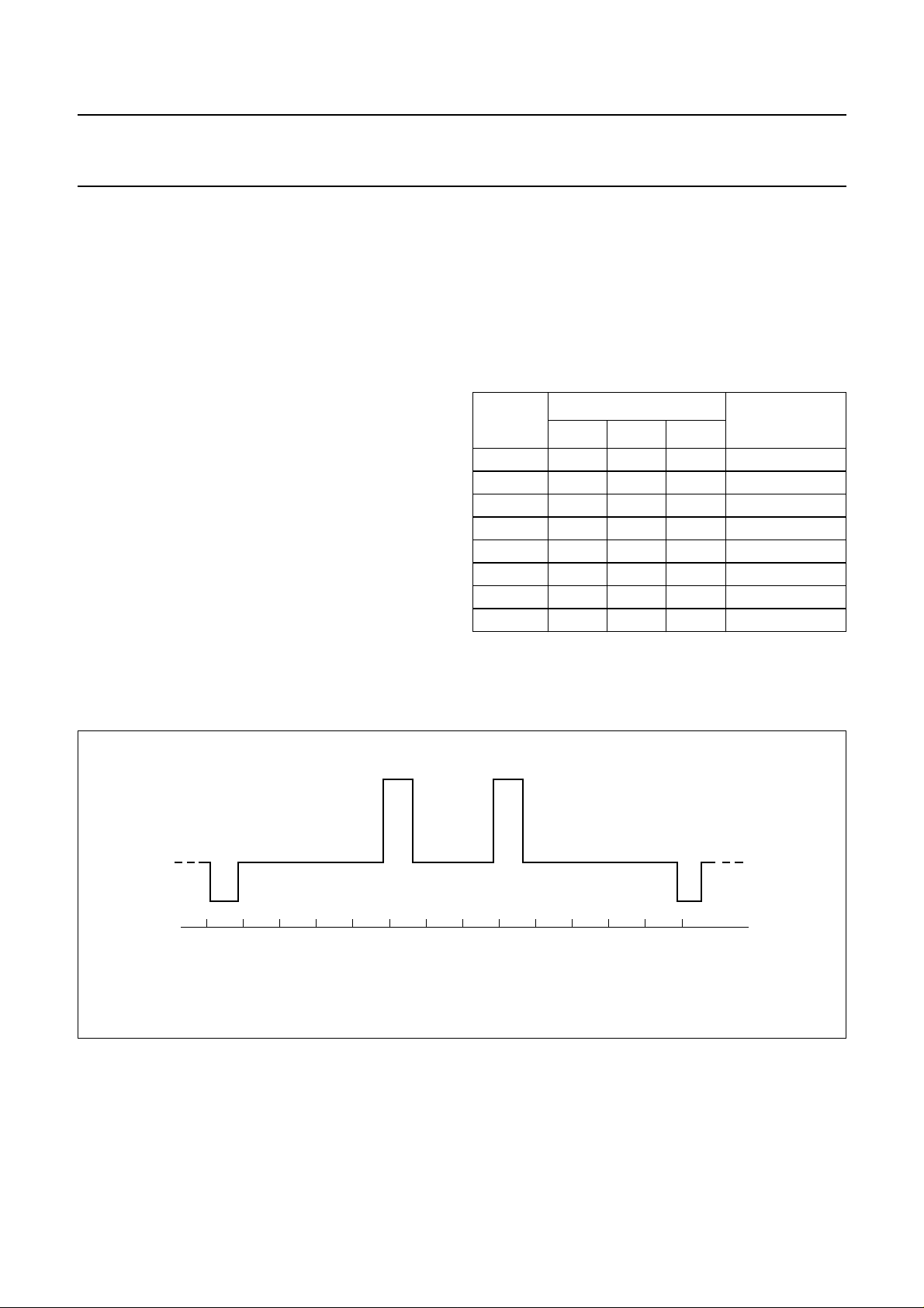
• The video part also contains a TPSG. This TPSG
generates a pattern that helps to tune the TV set to the
programmed channel of the modulator. The pattern
consists of a sync pulse and two vertical white bars on
the screen (see Fig.3)
2
C-bus programming, called MD2,
TDA8822
The TPSG is activated in two ways:
– Forcing the pin TPSG to DGND in the application
(see Fig.8)
– Setting the TPSG bit to 1 via the I2C-bus, then the
TPSG pin acts as an output port, sinking current to
allow the indication of the use of the TPSG in the
application e.g. with an LED (see Fig.9).
Table 1 Modulation depth setting (typical values)
MD
SETTING
0 0 0 0 72.5
1 0 0 1 75.0
2 0 1 0 77.5
3 0 1 1 80.0
4 1 0 0 82.5
5 1 0 1 85.0
6 1 1 0 87.5
7 1 1 1 90.0
MD2 MD1 MD0
BIT
MODULATION
DEPTH (%)
handbook, full pagewidth
0 5 10 15 20 25 30 35 40 45 50 55 60 65 t (µs)
Fig.3 Test pattern signal.
1997 Jan 08 6
MGE675
Philips Semiconductors Preliminary specification
Universal I2C-bus programmable RF
modulator
Audio part
The audio part provides the following:
• The sound subcarrier is created in an integrated VCO.
The signal at the output of this VCO is fed to a stage that
adjusts the picture-to-sound ratio and to the audio
programmable divider.
• The frequency of the sound subcarrier is set by
programming the bits SC1 and SC0 of the I2C-bus (see
Table 2). These two bits set the dividing ratio of the
audio programmable divider to get the divided frequency
f
div(audio)
• The audio phase detector compares the
phase/frequency of the divided audio frequency f
and the reference frequency for the audio, f
drives the Charge Pump (CP) that charges or
discharges the audio loop filter connected between
pins ACP and AGND to get the VCO oscillating to the
programmed frequency.
.
div(audio)
ref(audio)
and
TDA8822
• f
ref(audio)
purpose output port during a special test mode.
• The frequency deviation of the sound subcarrier is set
using 3 bits DEV2, DEV1 and DEV0 of the I2C-bus
programming (see Table 3), when a signal of 1 kHz with
a level of 50 mV (p-p) is applied on the audio input pin.
• The difference between the picture carrier level and the
sound subcarrier level is adjusted using 3 bits PS2, PS1
and PS0 (see Table 4).
• The NICAM amplifier has a constant gain, and is
designed for adding a second sound subcarrier in the TV
channel. This subcarrier can be either a second FM
carrier for dual-sound/stereo system used in PAL B/G or
a modulated NICAM carrier. The level between the
picture carrier and the NICAM carrier (P/N) will depend
on the input level on the NICAM input.
and f
div(audio)
can be monitored on the general
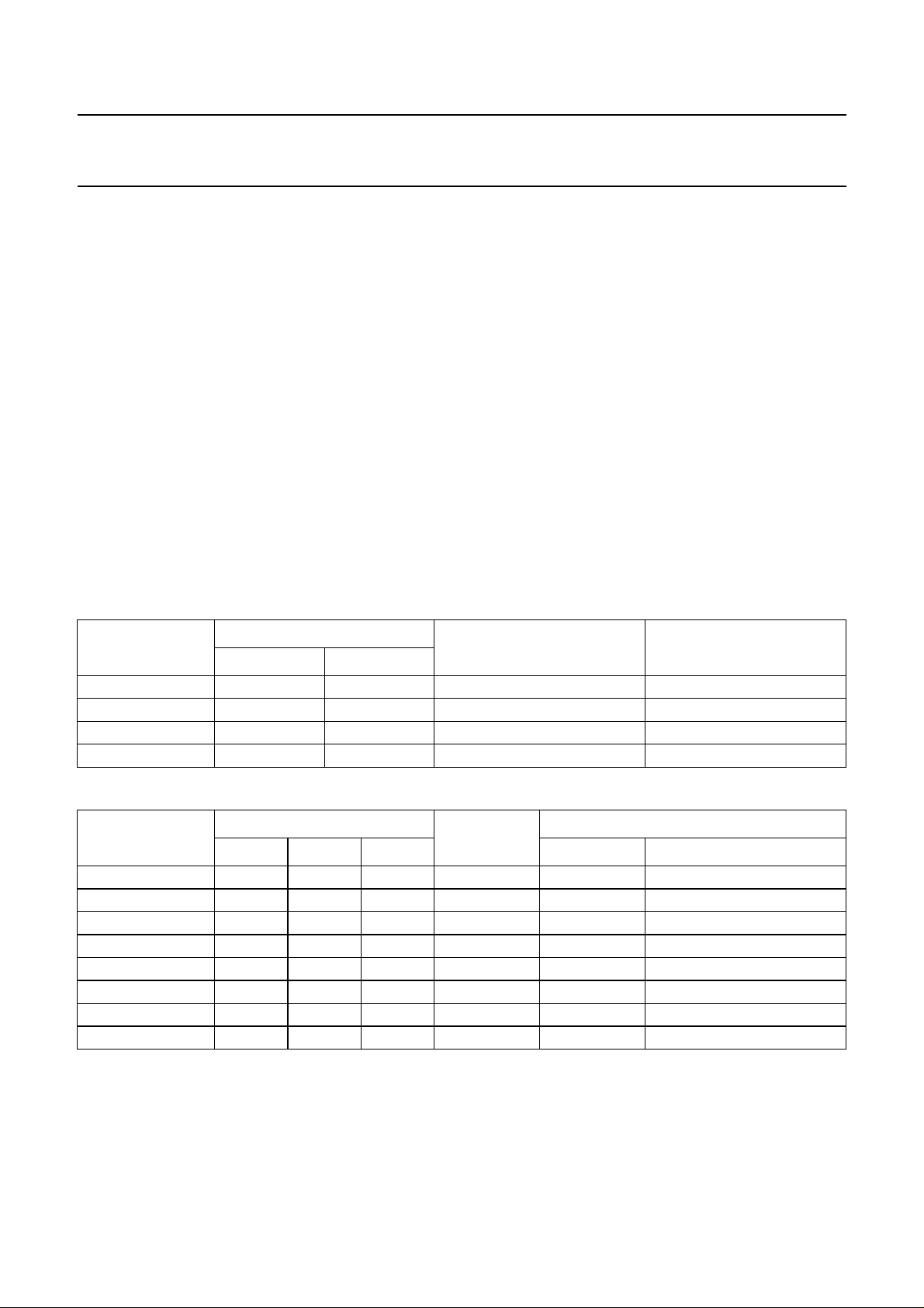
Table 2 Sound subcarrier frequency setting
SC SETTING
BIT
SC1 SC0
0 0 0 4.5 M, N
1 0 1 5.5 B, G
2 1 0 6.0 I
3 1 1 6.5 D, K
Table 3 Sound subcarrier frequency deviation setting (typical values)
BIT
DEV SETTING
DEV2 DEV1 DEV0 B, G, I, D, K M, N
0 0 0 0 40.0 20.0 10.0
1 0 0 1 45.0 22.5 11.3
2 0 1 0 50.5 25.3 12.6
3 0 1 1 56.5 28.3 14.1
4 1 0 0 63.5 31.8 15.9
5 1 0 1 71.5 35.8 17.9
6 1 1 0 80.0 40.0 20.0
7 1 1 1 90.0 45.0 22.5
SOUND SUBCARRIER
FREQUENCY (MHz)
DEVIATION
(%)
STANDARD
DEVIATION (kHz)
1997 Jan 08 7
Philips Semiconductors Preliminary specification
Universal I2C-bus programmable RF
modulator
Table 4 Picture-to-sound ratio setting (typical values)
PS SETTING
PS2 PS1 PS0
0 000 −11
1 001 −12
2 010 −13
3 011 −14
4 100 −15
5 101 −16
6 110 −17
7 111 −18
RF part
The RF part provides the following:
• The RF oscillator can produce any frequency used for
TV transmission, from 35 to 890 MHz. The frequency
range depends on the components used in the
application (see Table 11).
• The RF mixer combines the video signal, the sound
subcarrier and the carrier from the NICAM input to build
a baseband TV channel. This baseband signal is then
mixed with the RF oscillator signal to get the RF TV
channel.
• The two signals from the RF mixer are sent to the output
buffer. This output buffer can be used either as two
asymmetrical outputs or as one symmetrical output.
• The output buffer is switched-off while the PLL is not
in-lock, to avoid parasitic output signal during the tuning
of the RF oscillator. The in-lock information is given by
the phase detector of the loop.
• The signal from the RF oscillator is fed to the PLL which
controls the picture carrier frequency. The RF signal is
first divided by 8 in the prescaler, and then divided in the
programmable 14-bits divider. The dividing ratio of this
divider is programmed via the I2C-bus. The minimum
frequency that can be synthesized is 16 MHz, and the
maximum frequency is 1023.9375 MHz.
• The divided frequency called f
reference frequency called f
div(video)
ref(video)
is compared to the
coming from the
crystal oscillator and divided in the reference divider.
The crystal oscillator is intended to be used with a
crystal of 4 MHz.
• The comparison between f
ref(video)
and f
div(video)
in the video phase detector. The resulting signal is fed
via the video charge pump to the loop amplifier,
including the tuning voltage drive (33 V) inside the IC.
BIT
is done
TDA8822
P/S RATIO
(dB)
• f
ref(video)
and f
div(video)
output port during a special test mode.
• The I2C-bus receiver and control logic includes the
control of:
– Picture carrier frequency
– Sound subcarrier frequency
– Sound subcarrier frequency deviation
– Video modulation depth
– Picture-to-sound ratio
– TPSG on/off and LED drive control
– RF oscillator on/off
– Sound oscillator on/off
– General purpose output port on/off
– Test modes setting.
Software information
The transmission is made using 4 words in I
First the address CA has to be sent, then at least two
consecutive words have to be sent, either the two words
F1 and F0, or the two words C1 and C0.
The two words C1 and F1 are differentiated inside the IC
by the first bit being logic 1 or logic 0 respectively.
The contents of the 4 bytes is shown in Table 5.
At the power-up of the TDA8822, the I2C-bus state is the
following:
• N13 to N0 are not fixed
• SC setting = 1: the sound carrier is fixed to 5.5 MHz
• MD is set to 4 (82.5%), PS is set to 1 (−12 dB) and DEV
is set to 2 (50.5%)
can also be monitored on the
2
C-bus format.
1997 Jan 08 8

Philips Semiconductors Preliminary specification
Universal I2C-bus programmable RF
modulator
• T0 is set to logic 1, RF0 is set to logic 1, TPSG is set to
logic 1 and P0 is set to logic 0 to select the video high
impedance test mode because it is in this mode that the
RF oscillator starts in the best conditions.
The TPSG bit is used to switch on or off the TPSG using
the I2C-bus. It is also possible to switch the TPSG on in the
application, connecting the pin TPSG to DGND. This
pin TPSG has a double function and acts as an input or as
an output.
These are the two functions:
• Output: if the TPSG is set using the I2C-bus, the
pin TPSG is used as an output open collector NPN port.
This port can be used to indicate with an LED that the
TPSG is on. This is especially useful in systems using
an on-screen display. If the TV set is not tuned to the
right channel there is an alternate indication that the
TPSG is on (see Fig.9).
• Input: if the TPSG is set with an hardware switch in the
application, the TPSG pin is used as one of the inputs to
select the TPSG mode (see Fig.8).
Notice that if the TPSG bit is set to logic 1 while the RF0
bit is set to logic 0, the TPSG is turned off, and the sound
oscillator is off (see Table 8).
N13 to N0 are the 14 bits to set the video programmable
divider ratio and then to set the picture carrier frequency
following the formula: f
where:
• f
ref(video)
reference divider ratio. For example, with a 4 MHz
crystal connected to
pin XTAL,f
is the frequency on pin XTAL divided by the
ref video()
osc=fref(video)
4000000
----------------------- 512
× 8 × N,
7812.5 Hz==
TDA8822
• N is the programmable divider ratio:
N=N
• f
osc
DEV2, DEV1 and DEV0 are the bits to set the sound
subcarrier frequency deviation (see Table 3).
PS2, PS1 and PS0 are the bits to set the picture-to-sound
ratio (see Table 4).
MD2, MD1 and MD0 are the bits to set the modulation
depth (see Table 1).
SC1 and SC0 are the bits to set the sound subcarrier
frequency according to Table 2.
RF0 is a bit that controls the RF oscillator on/off. In normal
mode, it should be set to logic 1. If the modulator is not
used and may create some interferences with other
signals in the application, it should be set to logic 0
(see Table 6).
Notice that if the bit RF0 is logic 0 while the bit TPSG is
logic 1, then the RF oscillator is still running, but the sound
oscillator is off, and the TPSG is also off (see Table 8).
The bit P0 controls the output port P0, which is an open
collector NPN port, able to drive up to 10 mA
(see Table 7).
T0 is a bit used for test purposes. If this bit is set to logic 0,
the IC operates in normal configuration. If it is set to
logic 1, then the use of bits TPSG, RF0 and P0 is changed
to select 1 of the 8 test modes as explained in Table 9.
× 213+N12× 212+ ... + N1× 2+N
13
is the RF oscillator frequency.
0
Table 5 Contents of programming words
BYTE
Address byte CA 11001010 ACK
F1: frequency
byte 1
F0: frequency
byte 0
C1: control byte 1 1 DEV2 DEV1 DEV0 PS2 PS1 PS0 0 ACK
C0: control byte 0 MD2 MD1 MD0 SC1 SC0 RF0 P0 T0 ACK
1997 Jan 08 9
MSB LSB
ACKNOWLEDGE BIT
BIT 7 BIT 6 BIT 5 BIT 4 BIT 3 BIT 2 BIT 1 BIT 0
0 TPSG N13 N12 N11 N10 N9 N8 ACK
N7 N6 N5 N4 N3 N2 N1 N0 ACK
 Loading...