

Philips TDA8808AT, TDA8808T Datasheet

INTEGRATED CIRCUITS
DATA SH EET
TDA8808T
TDA8808AT
Photo diode signal processor for
compact disc players
Product specification
File under Integrated Circuits, IC01
November 1987

Philips Semiconductors Product specification
Photo diode signal processor for
compact disc players
TDA8808T
TDA8808AT
GENERAL DESCRIPTION
The TDA8808 is a bipolar integrated circuit designed for use in compact disc players with a single spot read-out system.
It amplifies the photo-diode signals and processes the error signals for the focus- and radial control network.
Features
• Data amplifier with equalizer and AGC
• Offset-free pre-amplifier with AGC for the servo signals
• Trackloss and drop-out detection
• Start-up procedure for focus
• Normalizing focus error output signal to minimize radial error interference
• Laser supply amplifier and reference source
• Both TDA8808T and TDA8808AT versions suitable for car, portable and home applications
• Single and dual supply application
• Focus in-lock signal; ready signal output (RD).
QUICK REFERENCE DATA
SYMBOL PARAMETER CONDITIONS MIN. TYP. MAX. UNIT
Supply
V
P
Supply voltage range 4,5 5,0 5,5 V
External voltage range
V
ext
V
ext
I
Q
TDA8808T −5,5 −5,0 0 V
TDA8808AT V
P
10 12 V
Quiescent supply current Si/RD = 0 V 7,5 10 12,5 mA
HF input current
I
HFin(p-p)
(peak-to-peak value) f
= 100 kHz 3 − 10 µA
HFin
LF input current
I
D
I
LO
(for each diode input) 0 − 6 µA
Laser supply output current Si/R7D = HIGH Z −8 −4 −2mA
Operating ambient
T
amb
temperature range −30 −+85 °C
PACKAGE OUTLINE
28-lead mini-pack; plastic (SO28; SOT136A); SOT136-1; 1996 August 13.
November 1987 2
Philips Semiconductors Product specification
Photo diode signal processor for compact
disc players
TDA8808T
TDA8808AT
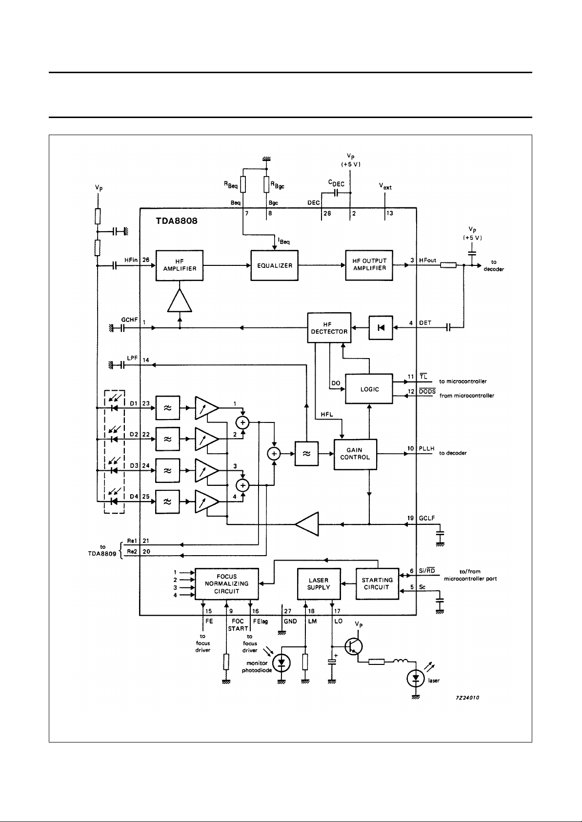
Fig.1 Block diagram.
November 1987 3
Philips Semiconductors Product specification
Photo diode signal processor for compact
disc players
PINNING
TDA8808T
TDA8808AT
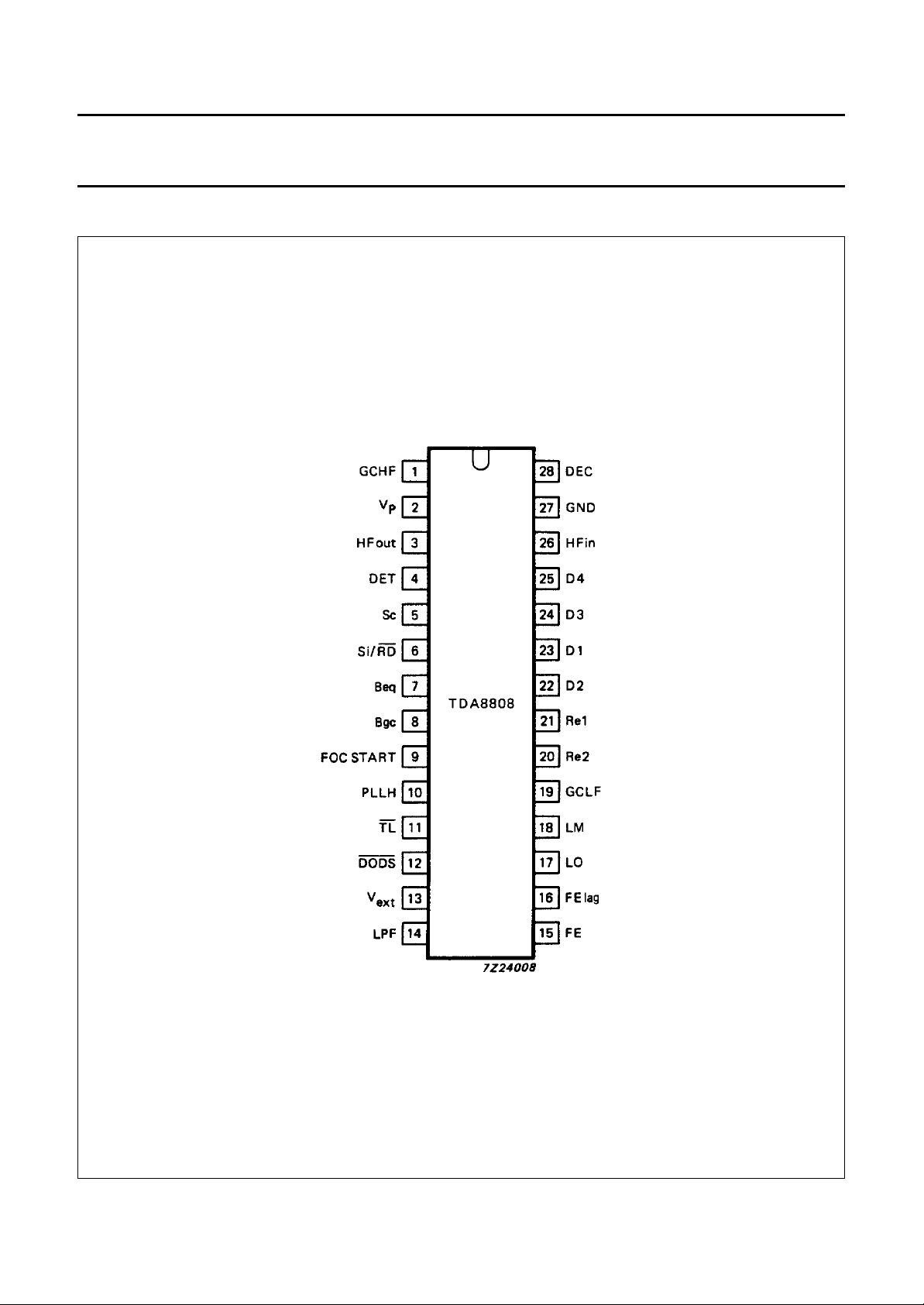
Fig.2 Pinning diagram.
November 1987 4

Philips Semiconductors Product specification
Photo diode signal processor for compact
disc players
Pin functions
PIN MNEMONIC DESCRIPTION
1 GCHF Gain control input of HF amplifier. Current output from HF amplitude detector
2V
3 HFout HF amplifier and equalizer voltage output
4 DET HF detector voltage input
5 Sc Starting up capacitor input
6 Si/
7 Beq Equalizer reference current input
8 Bgc DC and LF gain control reference current input
9 FOC START Focus normalizing circuit starting current
10 PLLH PLL on hold output
11
12
13 V
14 LPF Low pass filter for I
15 FE Current output of normalized, switched focus error signal
16 FElag Current output of switched focus error signal, intended for lag network.
17 LO Laser amplifier current output
18 LM Laser monitor diode input
19 GCLF Gain control input for AC and LF amplifiers. Current output from LF amplitude detector
20 Re2 Summation of amplified currents from D3 and D4
21 Re1 Summation of amplified currents from D1 and D2
23, 22 D1, D2 Current inputs to DC and LF photo diode amplifier
24, 25 D3, D4 Current inputs to DC and LF photo diode amplifier
26 HFin Current input to HF amplifier
27 GND Ground connection of device: also substrate connection for TDA8808AT
28 DEC Decoupling input (internal bypass)
P
RD On/off control (start input); ready signal output (starting up procedure successful)
TL Track loss output
DODS Drop out detector suppression input
ext
Positive supply voltage
TDA8808T
Negative supply connection for FE and FElag output stage; also
substrate connection
TDA8808AT
Positive supply connection for FE and FElag output stage
, used in track loss (TL) detector and LF gain control
ret
TDA8808T
TDA8808AT
November 1987 5
Philips Semiconductors Product specification
Photo diode signal processor for compact
disc players
RATINGS
Limiting values in accordance with the Absolute Maximum System (IEC 134)
SYMBOL PARAMETER MIN. MAX. UNIT
Supply voltage ranges (see Fig.3)
TDA8808T
V
P−V(ext)
V
GND−V(ext)
V
ext−VGND
V
P−VGND
V
O
V
O
V
O
V
O
P
tot
T
stg
T
amb
T
j
pin 2 to pin 13 −0,3 13 V
pin 27 to pin 13 −0,3 13 V
TDA8808AT
pin 13 to 27 −0,3 13 V
pin 2 to pin 27 −0,3 13 V
Output voltage ranges
except FE and FE
FE and FE
FE and FE
lag
lag
lag
(TDA8808T) V
(TDA8808AT) V
LM (open loop) V
Total power dissipation see Fig.4
Storage temperature range −55 + 150 °C
Operating ambient temperature range −30 + 85 °C
Operating junction temperature − 150 °C
TDA8808T
TDA8808AT
0V
ext
GND
GND
P
V
P
V
ext
V
P
V
V
V
V
THERMAL RESISTANCE
From junction to ambient R
th j-a
= 140 K/W
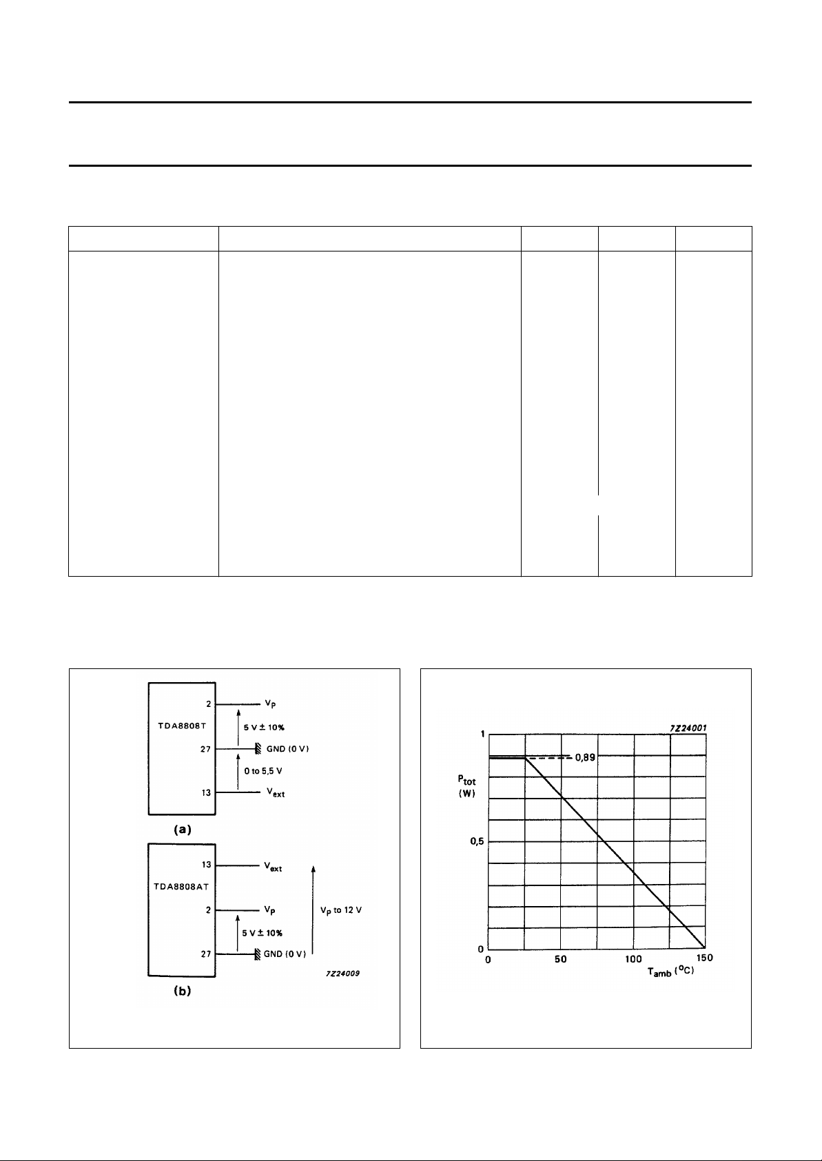
Fig.3 Supply voltages; (a) TDA8808T,
(b) TDA8808AT.
November 1987 6
Fig.4 Power derating curve.

Philips Semiconductors Product specification
Photo diode signal processor for compact
disc players
TDA8808T
TDA8808AT
CHARACTERISTICS
= + 5 V; V
V
P
(TDA8808T); V
all voltages measured with respect to V
GND
FE
= 0 V; V
= V
FElag
= −5 V (TDA8808T); V
ext
= 5 V (TDA8808A T); R
, unless otherwise specified
GND
= + 10 V (TDA8808AT); V
ext
FOC START
= 3,3 kΩ; I
Beq
= V
RE1
= I
= 50 µA (current sources); T
Bgc
= 3,5 V; VFE = V
RE2
FElag
= 25 °C;
amb
= 0 V
SYMBOL PARAMETER CONDITIONS MIN. TYP. MAX. UNIT
Supply
V
P
Supply voltage range 4,5 5,0 5,5 V
External voltage range
V
ext
V
ext
I
Q
TDA8808T −5,5 −5,0 0 V
TDA8808AT V
Quiescent supply current V
= 0 V 7,5 10 12,5 mA
Si/RD
P
10 12 V
Reference input (Beq)
V
I
Beq
Beq
Input voltage level 500 560 620 mV
Input current −−50 −µA
Reference input (Bgc)
V
I
Bgc
Bgc
Input voltage level 1,15 1,25 1,35 V
Input current −−50 −µA
Decoupling input (DEC)
V
Z
DEC
DEC
Input voltage level − VP−1,4 − V
Input impedance − 2 − kΩ
HF input (HFin)
V
HFin
Input voltage level − 1,4 − V
HF input current
I
HFin(p-p)
Input impedance 0,5 1 2 kΩ
Z
HFin
(peak-to-peak value) f
= 100 kHz 3 − 10 µA
HFin
HF part
DC characteristics
= ± 1 µA
I
V
∆
HFout
Gain G1()
=
---------------------
∆
I
HFin
G1(max) Maximum gain V
G1(min) Minimum gain V
HFin
= 4 V 390 480 570 mV/µA
GCHF
= 1,5V −5 0 5 mV/µA
GCHF
AC characteristics
G2 note 1 2 3,5 5 dB
Gain G2()20
G3 note 2 4 5,5 7 dB
Gain G3()20
V
O1
----------log=
V
O2
V
O1
----------log=
V
O2
Phase of input/output signal
φ at 1 MHz note 3 −π/2 − rad.
November 1987 7
 Loading...