

Philips TDA8798HL-C1 Datasheet

DATA SH EET
Objective specification
Supersedes data of 1998 Apr 15
File under Integrated Circuits, IC02
1999 Sep 16
INTEGRATED CIRCUITS
TDA8798
Dual 8-bit, 100 Msps A/D converter
with DPGA
1999 Sep 16 2
Philips Semiconductors Objective specification
Dual 8-bit, 100 Msps A/D converter with
DPGA
TDA8798
FEATURES
• Dual 8-bit Analog-to-Digital Converter (ADC)
• Sampling rate up to 100 million samples per
second (Msps)
• Dual 34 dBV 6-bit Digitally Programmable Gain
Amplifier (DPGA) with optional power-off
• Optional external equalization filter with capacitive
coupling between DPGA and ADC
• Serial Interface (SI) for DPGA gain control using either
parallel load mode or count-up/count-down mode
• 3.3 V TTL/CMOS compatible I/O
• Differential or single-ended TTL/CMOS clock interface
• AC or DC coupling for DPGA inputs.
APPLICATIONS
• High-dynamic range acquisition front-ends
• Digital data storage read channels.
GENERAL DESCRIPTION
The TDA8798 is a dual 8-bit ADC with DPGA.
The 100 Mspsmaximumsamplingrateand34 dBVDPGA
gain range optimizes the ADC for high dynamic range
applications.
QUICK REFERENCE DATA
SYMBOL PARAMETER CONDITIONS MIN. TYP. MAX. UNIT
V
DDA
analog supply voltage 3.15 3.3 3.45 V
V
DDD
digital supply voltage 3.0 3.3 3.6 V
V
DDO
output stage supply voltage 2.7 3.3 3.6 V
I
DDA
analog supply current with DPGAEN LOW − 106 − mA
with DPGAEN HIGH − tbf − mA
I
DDD
digital supply current − 30 − mA
I
DDO
output stage supply current − 3 − mA
INL DC integral non-linearity from IC analog input to digital
output; ramp input;
f
CLK
= 100 MHz
with DPGA at G
(min)
−±3.0 tbf LSB
without DPGA −±1.0 tbf LSB
DNL DC differential non-linearity from IC analog input to digital
output; ramp input;
f
CLK
= 100 MHz
with DPGA at G
(min)
−±0.5 tbf LSB
without DPGA −±0.5 tbf LSB
V
n(o)(rms)
output referred noise (RMS value) DPGA at G
(max)
; Zi =50Ω;
noise bandwidth = 15 MHz
− tbf 2 mV
rms
B
(−3dB)(ADC)
ADC −3 dB analogue bandwidth at V
i(dif)(FS)
− 120 − MHz
B
(−3dB)(DPGA)
DPGA −3 dB bandwidth at V
i(dif)(max)
30 tbf − MHz
f
(sample)(max)
maximum sampling rate 100 −−Msps
P
tot
total power dissipation with DPGAEN LOW − 460 500 mW
with DPGAEN HIGH − tbf tbf mW
1999 Sep 16 3
Philips Semiconductors Objective specification
Dual 8-bit, 100 Msps A/D converter with
DPGA
TDA8798
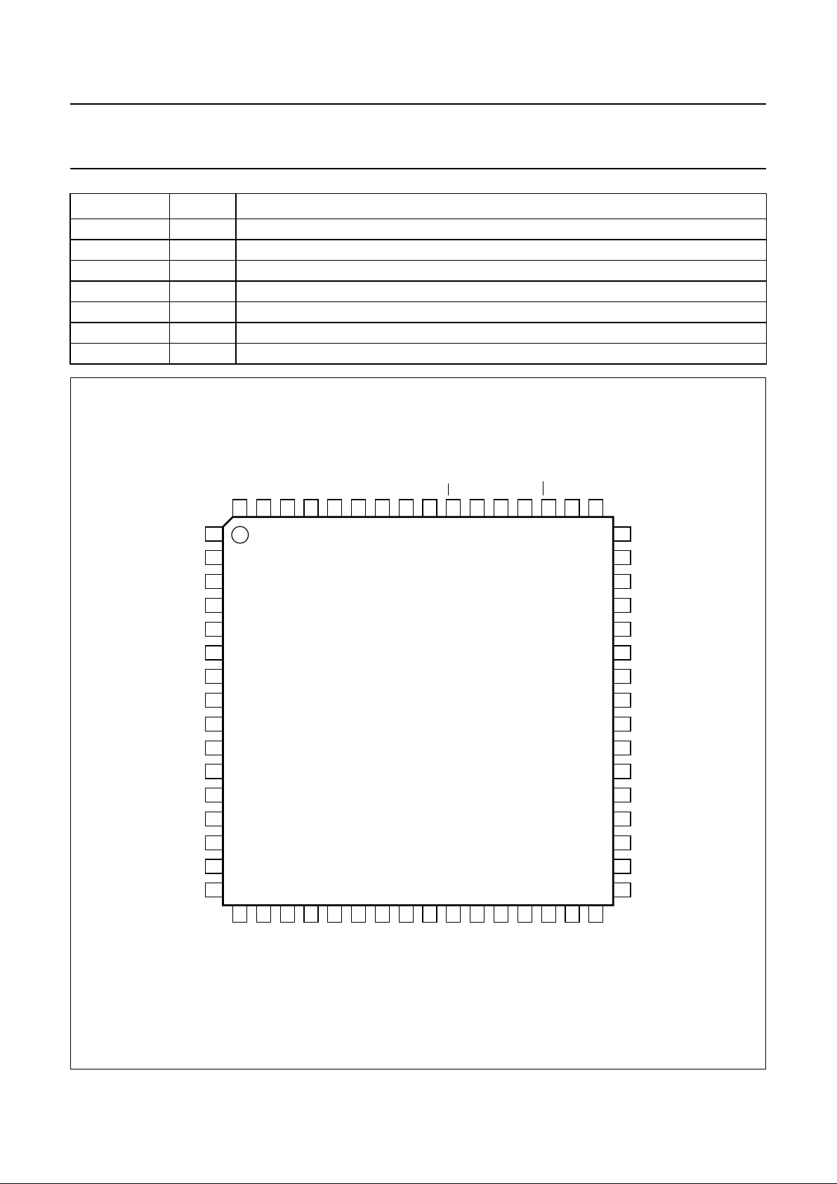
ORDERING INFORMATION
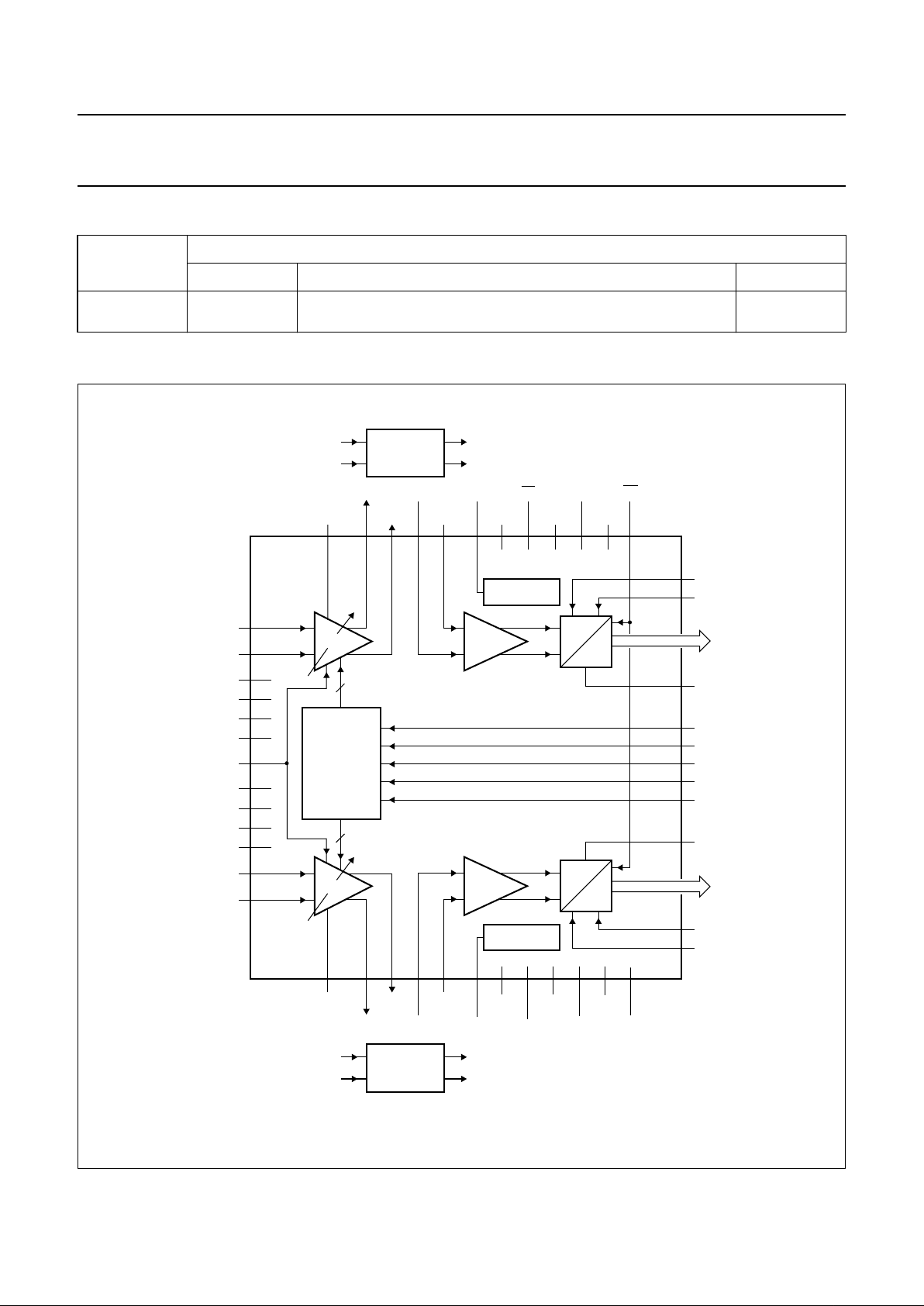
BLOCK DIAGRAM
TYPE
NUMBER
PACKAGE
NAME DESCRIPTION VERSION
TDA8798HL LQFP64 plastic low profile quad flat package; 64 leads;
body 10 × 10 × 1.4 mm
SOT314-2
Fig.1 Block diagram.
handbook, full pagewidth
MGM863
OPTIONAL
EXTERNAL
FILTER 2
SERIAL
INTERFACE
DPGA2
DPGA1
BUFFER
SR
58
59
52
V
DDA4
61 51
V
SSA4
6055
TEST
REGULATOR
54
V
oref2
V
oref1
62
BUF2
64
BUF2N
63
DPGA2N
1
DPGA2
to DPGA2
to DPGA2N
to BUF2
to BUF2N
OPTIONAL
EXTERNAL
FILTER 1
to DPGA1N
to DPGA1
to BUF1N
to BUF1
2
DPGAC2
V
DDO2
V
SSA3
BUF1DPGA1NDPGAC1
V
SSO1
V
DDO1
V
DDA3
BUF1NDPGA1
3
6
VIN2N
7
VIN2
10
VIN1
11
VIN1N
5
V
DDA2
8
V
SSA2
24
V
SSD1
25
V
DDD1
56
V
DDD2
53
DPGAEN
57
V
SSD2
9
V
SSA1
12
6
V
DDA1
325031212019
1718161514
41 to 48
4
29
26
28
30
13
40 to 33
23
22
CLK2N
CLK2
digital
output 2
B0 to B7
V
ref2
27
SEN2
SCLK
SMODE
SDATA
SEN1
V
ref1
digital
output 1
A0 to A7
analog
input 2
analog
input 1
CLK1
CLK1N
V
SSO2
49
BUFFER
TE
OE
A
D
A
D
TDA8798
REGULATOR
ADC1
ADC2
6
1999 Sep 16 4
Philips Semiconductors Objective specification
Dual 8-bit, 100 Msps A/D converter with
DPGA
TDA8798
PINNING
SYMBOL PIN DESCRIPTION
DPGA2N 1 DPGA2 inverting output
DPGA2 2 DPGA2 non-inverting output
DPGAC2 3 DPGA2 bandwidth limitation control
V
ref2
4 ADC2 reference output
V
DDA2
5 DPGA2 analog supply voltage
VIN2N 6 DPGA2 inverting input voltage
VIN2 7 DPGA2 non-inverting input voltage
V
SSA2
8 DPGA2 analog ground
V
SSA1
9 DPGA1 analog ground
VIN1 10 DPGA1 non-inverting input voltage
VIN1N 11 DPGA1 inverting input voltage
V
DDA1
12 DPGA1 analog supply voltage
V
ref1
13 ADC1 reference output
DPGAC1 14 DPGA1 bandwidth limitation control
DPGA1 15 DPGA1 non-inverting output
DPGA1N 16 DPGA1 inverting output
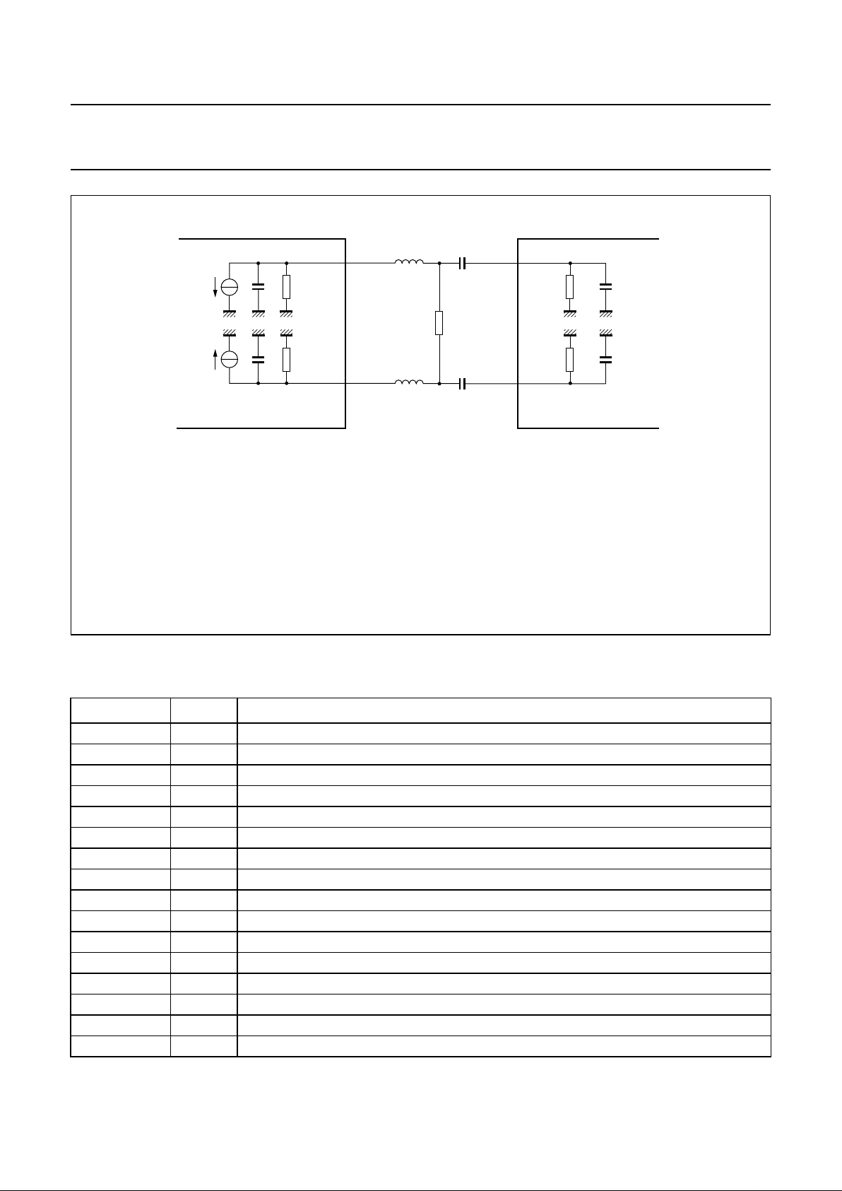
Fig.2 External filter.
External filtering may be used between DPGA and ADC to limit the noise bandwidth.
The external filterhasalow-passcut-offfrequency of .
and a high-pass cut-off frequency of
.
Other types of filter may be used if DC biasing is correct.
f
l 3dB–()
1
2π
------ -
R2⁄ R
oDPGA()
+
L
------------------------------------------
×≈
f
h 3dB–()
1
2π
------ -
1
R
iADC()
C×
----------------------------- -
×≈
(1) DPGA1/DPGA2
(2) BUF1/BUF2
(3) DPGA1N/DPGA2N
(4) BUF1N/BUF2N
handbook, full pagewidth
FCE267
I
OUT
−
I
OUT
C
o(DPGA)
TDA8798 TDA8798
10 µH
L
10 µH
100 nF
100 nF
C
C
L
C
o(DPGA)
R
o(DPGA)
DPGA
(1)
BUF
(2)
BUFN
(4)
R
1 kΩ
DPGAN
(3)
R
o(DPGA)
R
i(ADC)
R
i(ADC)
C
i(ADC)
C
i(ADC)
1999 Sep 16 5
Philips Semiconductors Objective specification
Dual 8-bit, 100 Msps A/D converter with
DPGA
TDA8798
BUF1 17 buffer1 non-inverting input
BUF1N 18 buffer1 inverting input
V
oref1
19 buffer1 common mode reference output
V
DDA3
20 ADC1 analog supply voltage 3
V
SSA3
21 ADC1 analog ground 3
CLK1N 22 ADC1 inverting clock input
CLK1 23 ADC1 non-inverting clock input
V
SSD1
24 digital ground 1
V
DDD1
25 digital supply voltage 1
SMODE 26 serial interface mode input
SEN2 27 serial interface enable 2 (active low)
SDATA 28 serial interface data input
SCLK 29 serial interface clock input
SEN1 30 serial interface enable 1 (active low)
V
DDO1
31 output stage supply voltage 1
V
SSO1
32 output stage ground 1
A7 33 channel 1 output bit 7 (MSB)
A6 34 channel 1 output bit 6
A5 35 channel 1 output bit 5
A4 36 channel 1 output bit 4
A3 37 channel 1 output bit 3
A2 38 channel 1 output bit 2
A1 39 channel 1 output bit 1
A0 40 channel 1 output bit 0 (LSB)
B0 41 channel 2 output bit 0 (LSB)
B1 42 channel 2 output bit 1
B2 43 channel 2 output bit 2
B3 44 channel 2 output bit 3
B4 45 channel 2 output bit 4
B5 46 channel 2 output bit 5
B6 47 channel 2 output bit 6
B7 48 channel 2 output bit 7 (MSB)
V
SSO2
49 output stage ground 2
V
DDO2
50 output stage supply voltage 2
OE 51 digital output enable (active LOW)
SR 52 digital output bit slew-rate control
DPGAEN 53 DPGA enable (active LOW)
TEST 54 test input (to be grounded)
TE 55 track-and-hold enable (active LOW)
V
DDD2
56 digital supply voltage 2
V
SSD2
57 digital ground 2
SYMBOL PIN DESCRIPTION
1999 Sep 16 6
Philips Semiconductors Objective specification
Dual 8-bit, 100 Msps A/D converter with
DPGA
TDA8798
CLK2 58 ADC2 non-inverting clock input
CLK2N 59 ADC2 inverting clock input
V
SSA4
60 ADC2 analog ground 4
V
DDA4
61 ADC2 analog supply voltage 4
V
oref2
62 buffer2 common mode reference output
BUF2N 63 buffer2 inverting input
BUF2 64 buffer2 non-inverting input
SYMBOL PIN DESCRIPTION
Fig.3 Pin configuration.
handbook, full pagewidth
TDA8798HL
MGM864
1
2
3
4
5
6
7
8
9
10
11
12
13
14
15
16
48
47
46
45
44
43
42
41
40
39
38
37
36
35
34
33
B7
B6
B5
B4
B3
B2
B1
B0
A0
A1
A2
A3
A4
A5
A6
A7
DPGA2N
DPGA2
DPGAC2
V
ref2
V
DDA2
VIN2N
VIN2
V
SSA2
V
SSA1
VIN1
VIN1N
V
DDA1
V
ref1
DPGAC1
DPGA1
DPGA1N
17
18
19
20
21
22
23
24
25
26
27
28
29
30
31
32
64
63
62
61
60
59
58
57
56
55
54
53
52
51
50
49
BUF2
BUF2N
V
oref2
V
DDA4
V
SSA4
CLK2N
CLK2
V
SSD2
V
DDD2
TEST
DPGAEN
SR
V
DDO2
V
SSO2
BUF1
BUF1N
V
oref1
V
DDA3
V
SSA3
CLK1N
CLK1
V
SSD1
V
DDD1
SMODE
SEN2
SDATA
SCLK
SEN1
V
DDO1
V
SSO1
TE
OE

1999 Sep 16 7
Philips Semiconductors Objective specification
Dual 8-bit, 100 Msps A/D converter with
DPGA
TDA8798
FUNCTIONAL DESCRIPTION
The TDA8798 comprises two independent fully differential
signalchainseachhavingaDPGAandahigh-speed ADC.
A serial interface allows the gain of each DPGA to be
controlledindependently. To improve signal conditions, an
AC-coupled external filter can be connected between a
DPGAandADC.TheTDA8798canbeused as a dual 8-bit
ADC without DPGA functionality, using less power.
Digitally Programmable Gain Amplifier (DPGA)
The gain of the differential DPGA is programmable from
0 to 34 dBV in 63 equal steps by a 6-bit word output in
parallel from a gain control register in the SI. For all gain
settings, the DPGA signal bandwidth exceeds 30 MHz.
The settling time between gain changes can be adjusted
by an external decoupling capacitor connected to
DPGAC1 (pin 14) and/or DPGAC2 (pin 3). The analog
input signals can be either AC or DC coupled. When used
only as a dual 8-bit ADC, both DPGAs can be disabled to
reduce power consumption.
Analog-to-Digital Converter (ADC)
The 8-bit ADC converts the differential analog input signal
into a binary output format at a maximum conversion rate
of 100 Msps. All digital input and output signals are
TTL/CMOS compatible.
The ADC clock signal can be from either a differential or a
single-ended source; when single-ended, the unused
clockinputpinshouldbe decoupled externally. The analog
input to the ADC is AC coupled.
Whenused only as a dualADC, the ADC can beexternally
biased by regulator output V
oref1
(pin 19) and/or
V
oref2
(pin 62) using series resistors of, for example, 50 Ω,
connected to the ADCbuffer inputs providing a lower input
impedance. This requires V
oref1
and/or V
oref2
to be
decoupled to ground by a 10 nF capacitor.
V
ref1
(pin 13) and/or V
ref2
(pin 4) provide a voltage
corresponding to the bias of the ADC which can be used
as a reference output to an external control circuit.
Alternatively, an external control voltage can be applied to
these pins to adjust the full-scale range of the ADC.
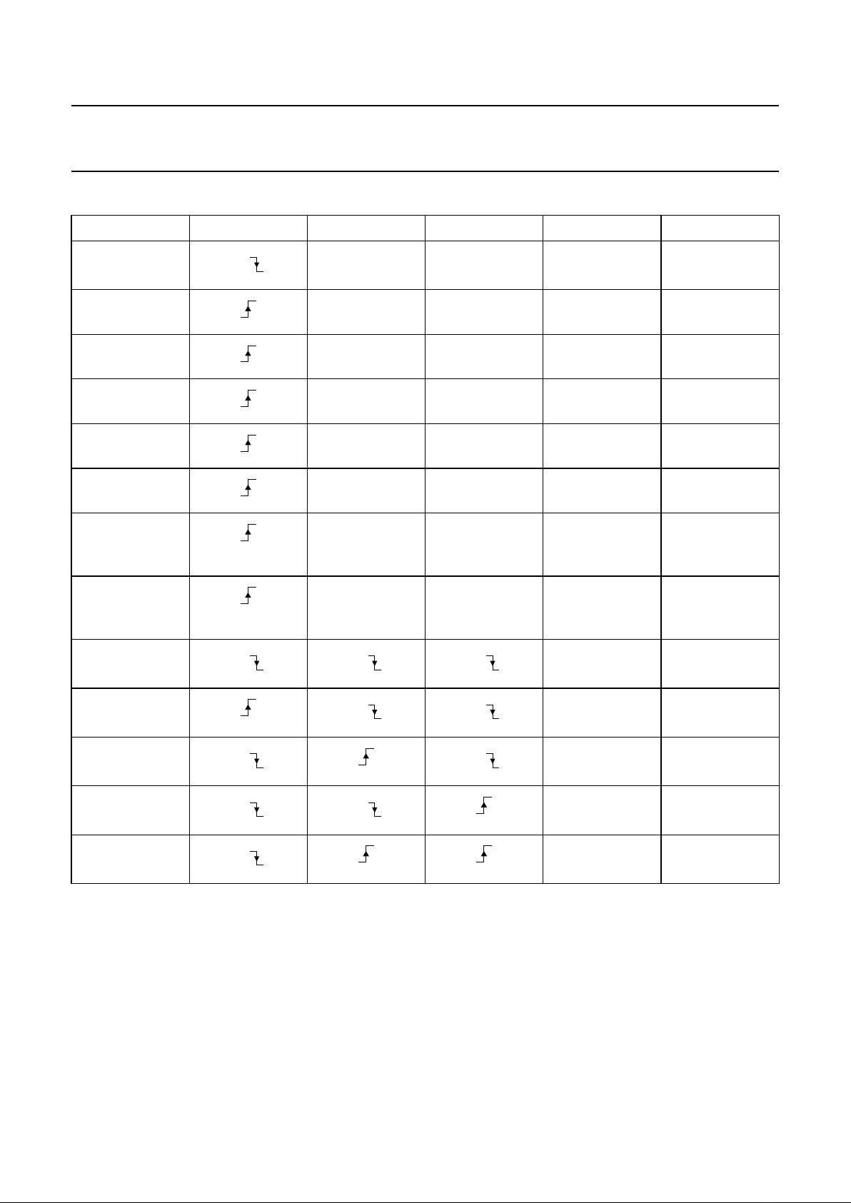
Serial Interface (SI)
The SI allows the gain of each DPGA to be controlled
independently using either a parallel load mode or a
count-up/count-down mode. The gain control mode is
selected by the state of SMODE. The operation of DPGA
gain control is shown in Timing diagram, (see Fig.4).
Parallel load mode
This mode loads gain control data serially into a decoder
in the SI. Each of the six bits are loaded on the rising edge
ofSCLK.After the load has completed, SEN goes inactive,
loading the data in parallel to a gain control register in the
SI, changing the gain of the DPGA.
Count-up/count-down mode
Count-up/count-down mode is selected when SMODE is
in the opposite state to parallel load mode. This mode
either increments or decrements the SI gain control
register in one-bit steps when SEN and SCLK are both
active; the state of SDATA determines the count direction
(up or down). This allows the gain of the DPGA to be
changed asynchronously and intermittently.
ADC digital outputs
Digital noise on the internal supply lines increases when
the V
DDO
voltage increases, affecting the crosstalk
between channels. This effect can be reduced by making
SR (pin 52) HIGH, changing the slew-rate of the ADC
digital outputs.
1999 Sep 16 8
Philips Semiconductors Objective specification
Dual 8-bit, 100 Msps A/D converter with
DPGA
TDA8798
Table 1 Serial interface truth table; see notes 1 and 2
Notes
1. ‘← Di’: shifting LSB and loading new LSB with value Di.
2. In count-up/count-down mode, thegain control register cannotbe incremented above themaximum gain value of 63,
or decremented below the minimum gain value of 0.
SMODE SCLK SEN1 SEN2 SDATA ACTION
0 1 1 U WAIT
0 1 1 Di SISR: SISR ← Di
0 0 1 1 SISR: SISR ← 1
GCR1: GCR1 + 1
0 0 1 0 SISR: SISR ← 0
GCR1: GCR1 − 1
0 1 0 1 SISR: SISR ← 1
GCR2: GCR2 + 1
0 1 0 0 SISR: SISR ← 0
GCR2: GCR2 − 1
0 0 0 1 SISR: SISR ← 1
GCR1: GCR1 + 1
GCR2: GCR2 + 1
0 0 0 0 SISR: SISR ← 0
GCR1: GCR1 − 1
GCR2: GCR2 − 1
1 U WAIT
1 Di SISR: SISR ← Di
1 U GCR1: SISR
1 U GCR2: SISR
1 U GCR1: SISR
GCR2: SISR
X,
X, X, X,
X, X,
X, X,
X, X,
X,
 Loading...