

Philips tda8705 DATASHEETS

INTEGRATED CIRCUITS
DATA SH EET
TDA8705
6-bit high-speed dual
Analog-to-Digital Converter (ADC)
Product specification
Supersedes data of November 1994
File under Integrated Circuits, IC02
1996 Jan 12
Philips Semiconductors Product specification
6-bit high-speed dual Analog-to-Digital
Converter (ADC)
FEATURES
• 2 times 6-bit resolution
• Sampling rate up to 40 MHz
• High signal-to-noise ratio over a large analog input
frequency range (5.8 effective bits at 10 MHz full-scale
input at f
• TTL output
• Two separated inputs (AC-coupling)
• TTL compatible digital inputs
• Low-level AC clock input signal allowed
• Internal reference voltage regulator
(external reference regulation possible)
• Power dissipation only 250 mW (typical)
• Low analog input capacitance, no buffer amplifier
required
• No sample-and-hold circuit required.
= 40 MHz
clk
TDA8705
APPLICATIONS
High-speed analog-to-digital conversion for:
• DBS (Digital Broadcast Satellite)
• QPSK (Quadrature Phase Shift Keying) demodulation
• Video.
GENERAL DESCRIPTION
The TDA8705 is a 6-bit high-speed dual analog-to-digital
converter (ADC) for satellite video and other applications.
It converts the two analog input signals into two 6-bit
binary-coded digital words at a maximum sampling rate of
40 MHz. All digital inputs and outputs are TTL compatible,
although a low-level sine wave clock input signal is
allowed.
QUICK REFERENCE DATA
SYMBOL PARAMETER CONDITIONS MIN. TYP. MAX. UNIT
V
V
V
I
CCA
I
CCD
I
CCO
CCA
CCD
CCO
analog supply voltage 4.75 5.0 5.25 V
digital supply voltage 4.75 5.0 5.25 V
output stages supply voltage 4.75 5.0 5.25 V
analog supply current 20 27 32 mA
digital supply current 10 14 18 mA
output stages supply current 10 14 18 mA
ILE DC integral linear error −±0.25 ±0.5 LSB
DLE DC differential linearity error −±0.25 ±0.5 LSB
AILE AC integral linearity error note 1 −±0.5 ±1.0 LSB
f
clk(max)
P
tot
maximum clock frequency 40 −−MHz
total power dissipation − 250 − mW
Note
1. Full-scale sine wave (f
= 10 MHz; f
i
= 40 MHz).
clk
ORDERING INFORMATION
TYPE
NUMBER
NAME DESCRIPTION VERSION
PACKAGE
TDA8705T SO28 plastic small outline package; 28 leads; body width 7.5 mm SOT136-1
1996 Jan 12 2
Philips Semiconductors Product specification
6-bit high-speed dual Analog-to-Digital
Converter (ADC)
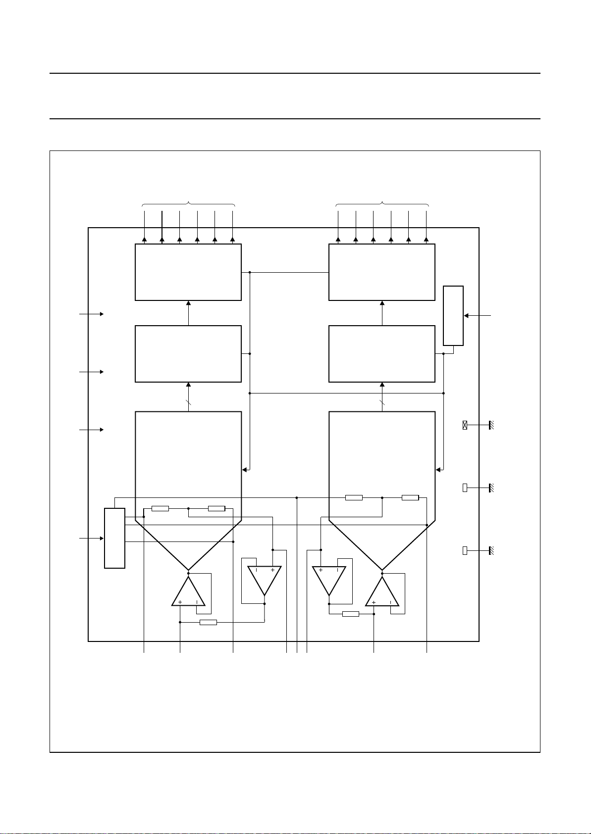
BLOCK DIAGRAM
data
outputs
D2A
D3A
25
26
TTL OUTPUTS
LATCHES
24 D1A
LSB
D0A
23
CCO
V
CCD
V
MSB
D5A
28
D4A
27
TDA8705
MSB
D5B
20
D4B
19
data
outputs
D2B
D3B
17
18
TTL OUTPUTS
LATCHES
16 D1B
TDA8705
LSB
D0B
15
MLC113
1
CLK
CLOCK DRIVER
CCA
V
DEC
8 2 21
10
REGULATOR
RTA
V
reference
voltage TOP
6
CONVERTER
ANALOG -TO-DIGITAL
6
IA
V
A
A
analog
voltage input
6
DGND
3
digital ground
A
INTA
R
4
RBA
V
A
reference
voltage BOTTOM
9512
RMA
V
A
reference
voltage MIDDLE
14
RTB
RMB
V
V
B
reference
voltage TOP
INTB
R
B
reference
voltage MIDDLE
B
CONVERTER
ANALOG -TO-DIGITAL
11
IB
V
B
analog
voltage input
13
RBB
V
B
reference
voltage BOTTOM
7
22
AGND
OGND
handbook, full pagewidth
Fig.1 Block diagram.
analog ground
output ground
1996 Jan 12 3
Philips Semiconductors Product specification
6-bit high-speed dual Analog-to-Digital
Converter (ADC)
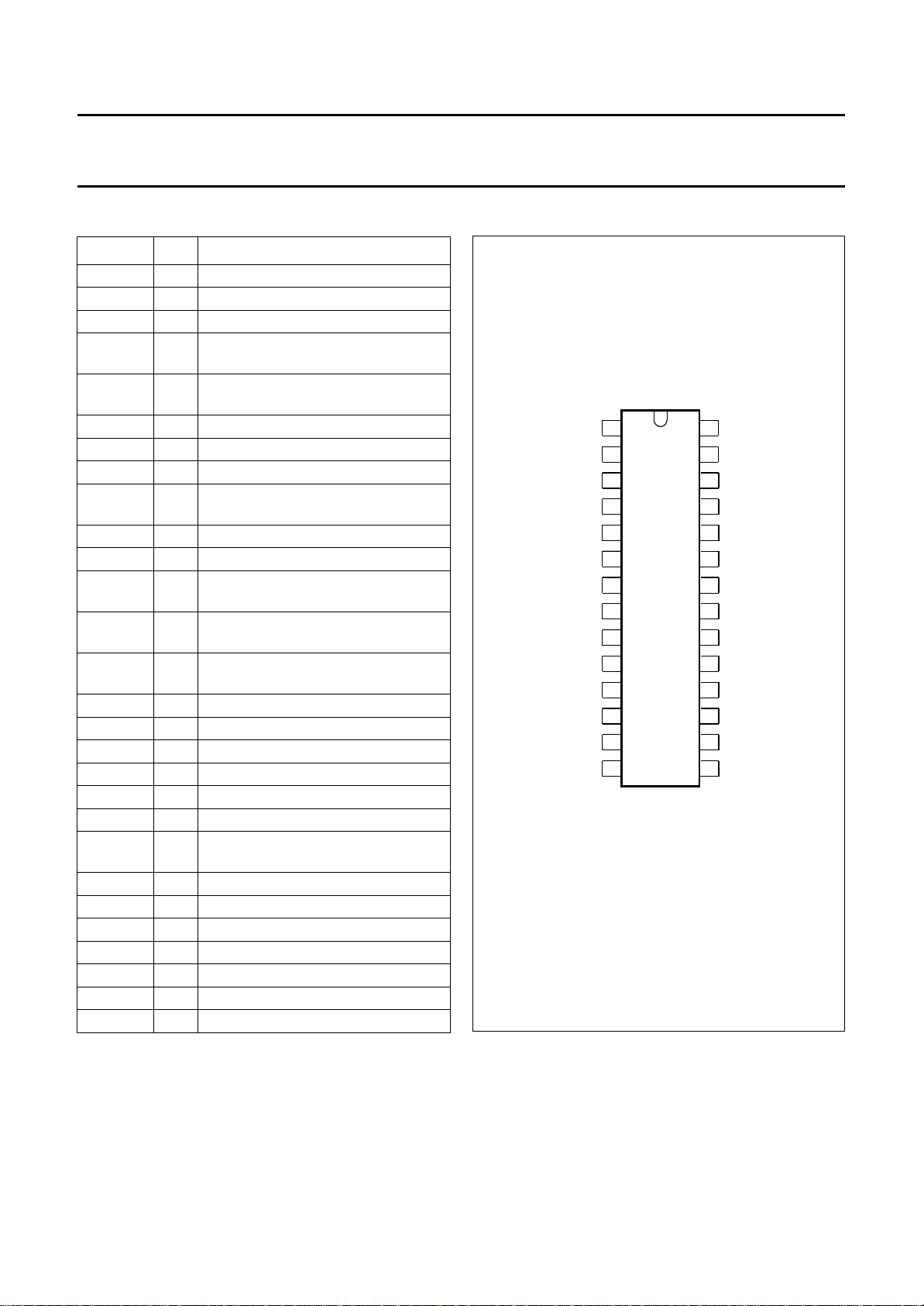
PINNING
SYMBOL PIN DESCRIPTION
CLK 1 clock input
V
CCD
DGND 3 digital ground
V
RBA
V
RTA
V
IA
AGND 7 analog ground
V
CCA
V
RMA
DEC 10 decoupling input
V
IB
V
RTB
V
RBB
V
RMB
D0B 15 data output; bit 0 (LSB), ADC B
D1B 16 data output; bit 1, ADC B
D2B 17 data output; bit 2, ADC B
D3B 18 data output; bit 3, ADC B
D4B 19 data output; bit 4, ADC B
D5B 20 data output; bit 5 (MSB), ADC B
V
CCO
OGND 22 output ground
D0A 23 data output; bit 0 (LSB), ADC A
D1A 24 data output; bit 1, ADC A
D2A 25 data output; bit 2, ADC A
D3A 26 data output; bit 3, ADC A
D4A 27 data output; bit 4, ADC A
D5A 28 data output; bit 5 (MSB), ADC A
2 digital supply voltage (+5 V)
4 reference voltage BOTTOM for
ADC A (decoupling)
5 reference voltage TOP for ADC A
(decoupling)
6 analog input voltage for ADC A
8 analog supply voltage (+5 V)
9 reference voltage MIDDLE for ADC A
(decoupling)
11 analog input voltage for ADC B
12 reference voltage TOP for ADC B
(decoupling)
13 reference voltage BOTTOM for
ADC B (decoupling)
14 reference voltage MIDDLE for ADC B
(decoupling)
21 supply voltage for output stages
(+5 V)
handbook, halfpage
1
CLK
V
2
CCD
3
DGND
V
4
RBA
V
5
RTA
V
6
IA
7
AGND
V
CCA
V
RMA
DEC
V
V
RTB
V
RBB
V
RMB
IB
TDA8705
8
9
10
11
12
13
MLC114
Fig.2 Pin configuration.
TDA8705
D5A
28
D4A
27
D3A
26
25
D2A
D1A
24
D0A
23
OGND
22
V
21
CCO
D5B
20
D4B
19
D3B
18
17
D2B
16
D1B
D0B
1514
1996 Jan 12 4
Philips Semiconductors Product specification
6-bit high-speed dual Analog-to-Digital
Converter (ADC)
LIMITING VALUES
In accordance with the Absolute Maximum Rating System (IEC 134).
SYMBOL PARAMETER CONDITIONS MIN. MAX. UNIT
V
CCA
V
CCD
V
CCO
∆V
∆V
∆V
V
I
V
clk(p-p)
I
O
T
stg
T
amb
T
j
CC
CC
CC
analog supply voltage note 1 −0.3 +7.0 V
digital supply voltage note 1 −0.3 +7.0 V
output stages supply voltage note 1 −0.3 +7.0 V
supply voltage differences
between V
CCA
and V
CCD
supply voltage differences
between V
CCO
and V
CCD
supply voltage differences
between V
CCA
and V
CCO
−1.0 +1.0 V
−1.0 +1.0 V
−1.0 +1.0 V
input voltage referenced to AGND −0.3 +7.0 V
AC input voltage for switching
referenced to DGND − V
CCD
(peak-to-peak value)
output current − 10 mA
storage temperature −55 +150 °C
operating ambient temperature 0 +70 °C
junction temperature − +150 °C
TDA8705
V
Note
1. The supply voltages V
between V
CCA
, V
CCO
CCA
and V
, V
and V
CCO
is between −1 V and +1 V.
CCD
may have any value between −0.3 V and +7.0 V provided the difference
CCD
HANDLING
Inputs and outputs are protected against electrostatic discharges in normal handling. However, to be totally safe, it is
desirable to take normal precautions appropriate to handling integrated circuits.
THERMAL CHARACTERISTICS
SYMBOL PARAMETER VALUE UNIT
R
th j-a
thermal resistance from junction to ambient in free air 70 K/W
1996 Jan 12 5
 Loading...