

Philips TDA8501T, TDA8501 Datasheet

INTEGRATED CIRCUITS
DATA SH EET
TDA8501
PAL/NTSC encoder
Preliminary specification
File under Integrated Circuits, IC02
April 1993

Philips Semiconductors Preliminary specification
PAL/NTSC encoder TDA8501
FEATURES
• Two input stages: R, G, B and −(R−Y), −(B−Y), Y with
multiplexing
• Chrominance processing, highly integrated, includes
low frequency filters for the colour difference signals,
and after the modulator a bandpass filter
• Fully controlled modulator produces a signal according
to the PAL or NTSC standard without adjustments
• A free running oscillator. Can be tuned by crystal or by
an external frequency source
• Output stages with separated Y + SYNC and
chrominance (Y + C, SVHS), and a CVBS output. Signal
amplitudes are correct for 75 Ω driving via an external
emitter follower. Internal generation of NTSC setup
• Sync separator circuit and pulse shaper, to generate the
required pulses for the processing, clamping, blanking,
FH/2, and burst pulse
• H/2 control pin. In PAL mode the internally generated
H/2 is connected to this pin and the phase of this signal
can be reset
• Internal bandgap reference.
GENERAL DESCRIPTION
The TDA8501 is a highly integrated PAL/NTSC encoder IC
which is designed for use in all applications where R, G
and B or Y, U and V signals require transformation to PAL
or NTSC values.The specification of the input signals are
fully compatible with the specification of those of the
TDA8505 SECAM-encoder.
ORDERING INFORMATION
EXTENDED TYPE
NUMBER
TDA8501 24 DIL plastic SOT234AH2
TDA8501T 24 SO plastic SOT137AH1
Note
1. SOT234-1; 1996 December 2.
2. SOT137-1; 1996 December 2.
PINS PIN POSITION MATERIAL CODE
PACKAGE
(1)
(2)
April 1993 2
Philips Semiconductors Preliminary specification
PAL/NTSC encoder TDA8501
April 1993 3
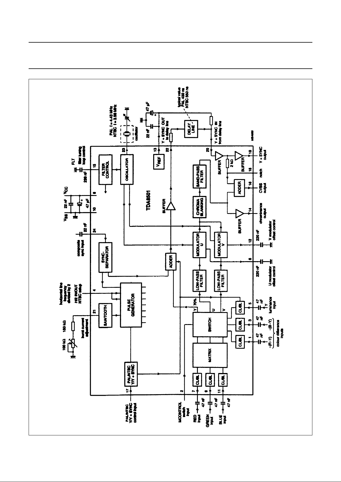
Fig.1 Block diagram.
Philips Semiconductors Preliminary specification
PAL/NTSC encoder TDA8501
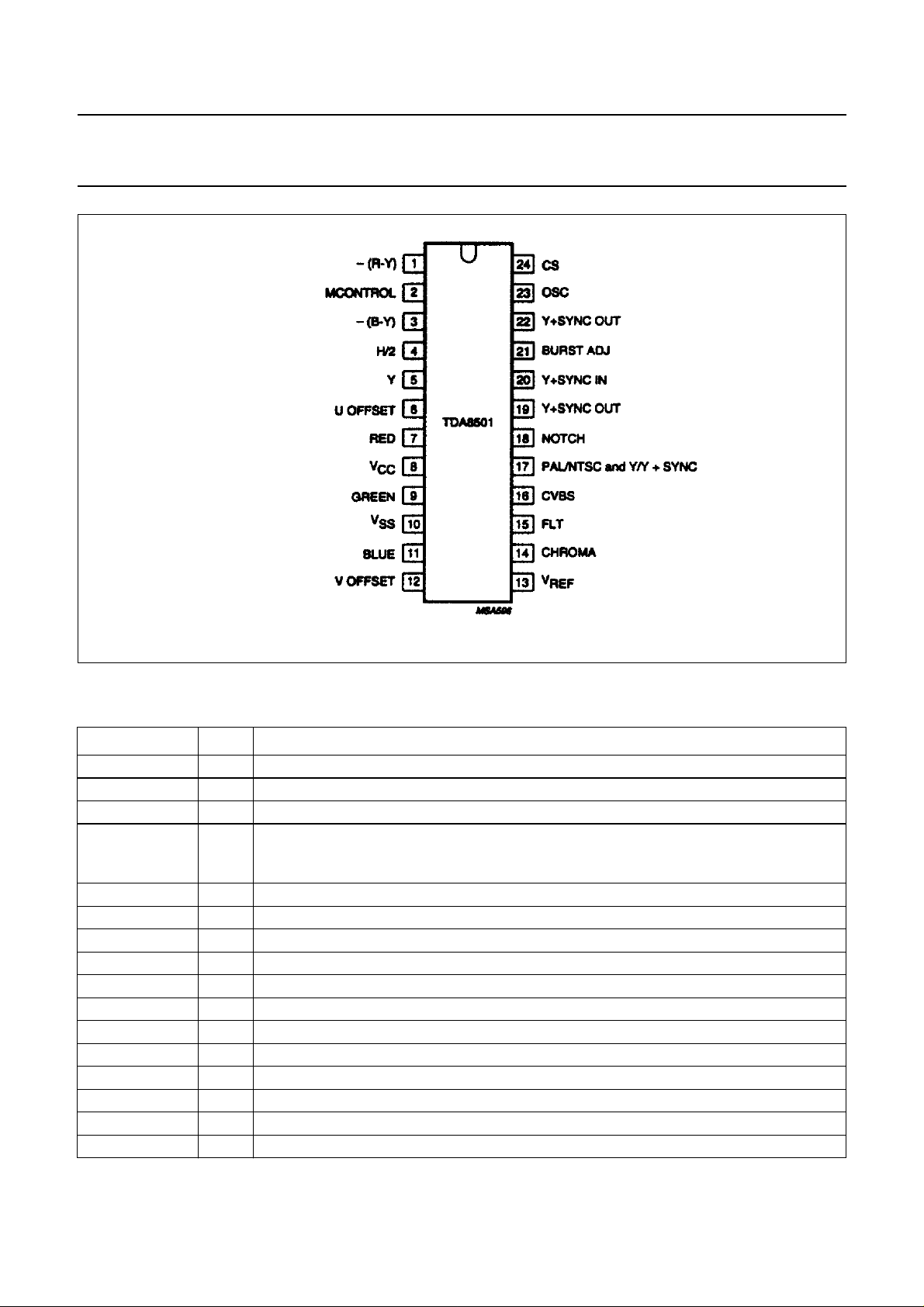
Fig.2 Pin configuration.
PINNING
U and V respectively, are the terms used to describe the colour difference signals at the output of the matrix.
SYMBOL PIN DESCRIPTION
−(R−Y) 1 colour difference input signal, for EBU bar (75%) 1.05 V (p-p)
MCONTROL 2 multiplexer switch control input; HIGH = RGB, LOW = −(R−Y), −(B−Y), Y
−(B−Y) 3 colour difference input signal, for EBU bar (75%) 1.33 V (p-p)
H/2 4 line pulse input/output divided-by-2 for synchronizing the internal H/2, if not used, this pin
dependent on mode selected, is either left open-circuit, or connected to VCC or to ground
(note 1)
Y 5 luminance input signal 1 V nominal without sync
U OFFSET 6 U modulator offset control capacitor
R 7 RED input signal for EBU bar of 75% 0.7 V (p-p)
V
CC
8 supply voltage; 5 V nominal
G 9 GREEN input signal for EBU bar of 75% 0.7 V (p-p)
V
SS
10 ground (0 V)
B 11 BLUE input signal for EBU bar of 75% 0.7 V (p-p)
V OFFSET 12 V modulator offset control capacitor
V
REF
13 2.5 V internal reference voltage output
CHROMA 14 chrominance output
FLT 15 filter tuning loop capacitor
CVBS 16 composite PAL or NTSC output, 2 V (p-p) nominal
April 1993 4
Philips Semiconductors Preliminary specification
PAL/NTSC encoder TDA8501
SYMBOL PIN DESCRIPTION
PAL/NTSC and
Y/Y + SYNC
NOTCH 18 Y +SYNC output via an internal resistor of 2 kΩ; a notch filter can be connected to this pin
Y +SYNC OUT 19 2 V (p-p) nominal Y +SYNC output
Y +SYNC IN 20 Y +SYNC input; (from pin 22) connected to the output of the external delay line
BURST ADJ 21 burst current adjustment via external resistor
Y +SYNC OUT 22 Y +SYNC output 1 V (p-p) nominal, connected to the input of the external delay line
OSC 23 oscillator tuning: connected to either a crystal in series with capacitor to ground, or to an
CS 24 composite sync input, 0.3 V (p-p) nominal
Notes
1. Pin 4: in PAL mode, if not connected to external H2 pulse, this pin is the output for the internally generated H/2 signal.
Pin 4: in NTSC mode, for internal set-up this pin is connected to ground; when internal set-up is switched off, this pin
is connected to VCC.
2. The listed voltages connected to pin 17 (if VCC = + 5 V) enable the following Y (via pin 5) input signal states:
0 V = PAL mode; at pin 5, Y without sync and input blanking on
5 V = NTSC mode; at pin 5, Y without sync and input blanking on
1.8 V = PAL mode; at pin 5, Y with sync and input blanking off
3.2 V = NTSC mode; at pin 5, Y with sync and input blanking off
17 four level control pin (note 2)
external frequency source via a resistor in series with a capacitor
April 1993 5

Philips Semiconductors Preliminary specification
PAL/NTSC encoder TDA8501
FUNCTIONAL DESCRIPTION
The TDA8501 device comprises:
• encoder circuit
• oscillator and filter control
• sync separator and pulse shaper.
Within this functional description, the term Y is used to
describe the luminance signal and the terms U and V
respectively, are used to describe the colour difference
signals.
Encoder circuit
INPUT STAGE
The input stage of the device uses two signal paths (see
Fig.1). Fast switching between the two signal paths is
achieved by means of the signal path selection switch
MCONTROL (pin 2).
AND G INPUT SIGNALS PATH
R, B
One signal path provides the connection for R, G and B
signal inputs (via pins 7, 9 and 11) which are connected to
a matrix via clamping and line blanking circuits. The signal
outputs from the matrix are U, V and Y.
For an EBU colour bar of 75% the amplitude of the signal
must be 0.7 V (peak-to-peak):
The Y input signal (via pin 5) differs from other signal
inputs, in that the timing of the internal clamp is after the
sync period.
The amplitude and polarity of these colour difference and
luminance input signals are processed to provide suitable
switch inputs of U, V and Y signal values.
The condition for 75% colour bar is:
pin 1 −(R−Y) = 1.05 V (peak-to-peak)
pin 3 −(B−Y) = 1.33 V (peak-to-peak)
pin 5 Y = 1 V (peak-to-peak) without sync
When selected (via MCONTROL), the U and V signals (via
the switch) are routed to the low pass filters. The Y signal
(via the switch) is routed via the adder and buffer to pin 22
(Y +SYNC OUT to delay line). Dependent on pin 17
conditioning, the Y signal may have external or internal
sync added (see section Four level control pin).
F
OUR LEVEL CONTROL PIN
The Y input signal (via pin 5) is conditioned by use of the
4-level control pin (pin 17) to emulate either the PAL or
NTSC modes, with sync and input blanking off or without
sync and input blanking on.
U = 0.493 (B−Y)
V = 0.877 (R−Y)
Y = 0.299 R +0.587 G +0.114 B
When selected (via MCONTROL), the U, V signals from
the matrix are routed through the selection switch to the
low pass filters. The Y signal from the matrix is routed
through the selection switch to the adder and combined
with the sync pulse from the sync separator and then
connected via a buffer internally to pin 22 (Y + SYNC OUT
to delay line).
−(R−Y), −(B−Y)
AND Y INPUT SIGNALS PATH
A second signal path provides the connection for negative
colour difference signal inputs−(R−Y),−(B−Y) i.e. V, U (via
pins 1, 3) and luminance Y (via pin 5), which are routed
directly to the switch inputs via clamping and line blanking
circuits.
Pin 17 may be hard wire connected to either ground (LOW
for PAL mode) or VCC (HIGH for NTSC mode). External
resistors can further modify the voltage level input at pin 17
to condition (pin 5) Y with sync and input blanking off or Y
without sync and input blanking on. (see section
PAL/NTSC and Y/Y +SYNC).
AND V SIGNALS
U
In PAL and NTSC modes the U and V (colour difference)
signals at the output of the switch are configured differently
as follows:
PAL mode:
• after the adding of the burst pulse to U and V, these
signals are connected to the input of the low pass filters.
During the vertical sync period the burst pulse is
suppressed.
NTSC mode:
• the burst pulse is only added to U and the gain of the U
and V signals is 0.95 of the gain in PAL mode. During
the vertical sync period the burst pulse is suppressed.
April 1993 6
Philips Semiconductors Preliminary specification
PAL/NTSC encoder TDA8501
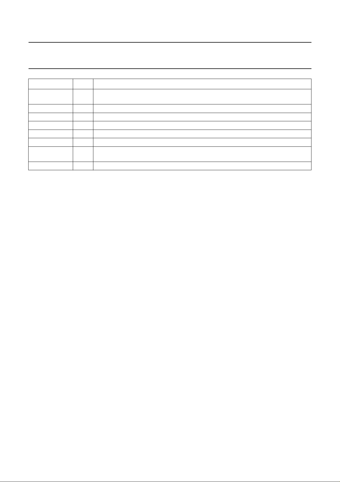
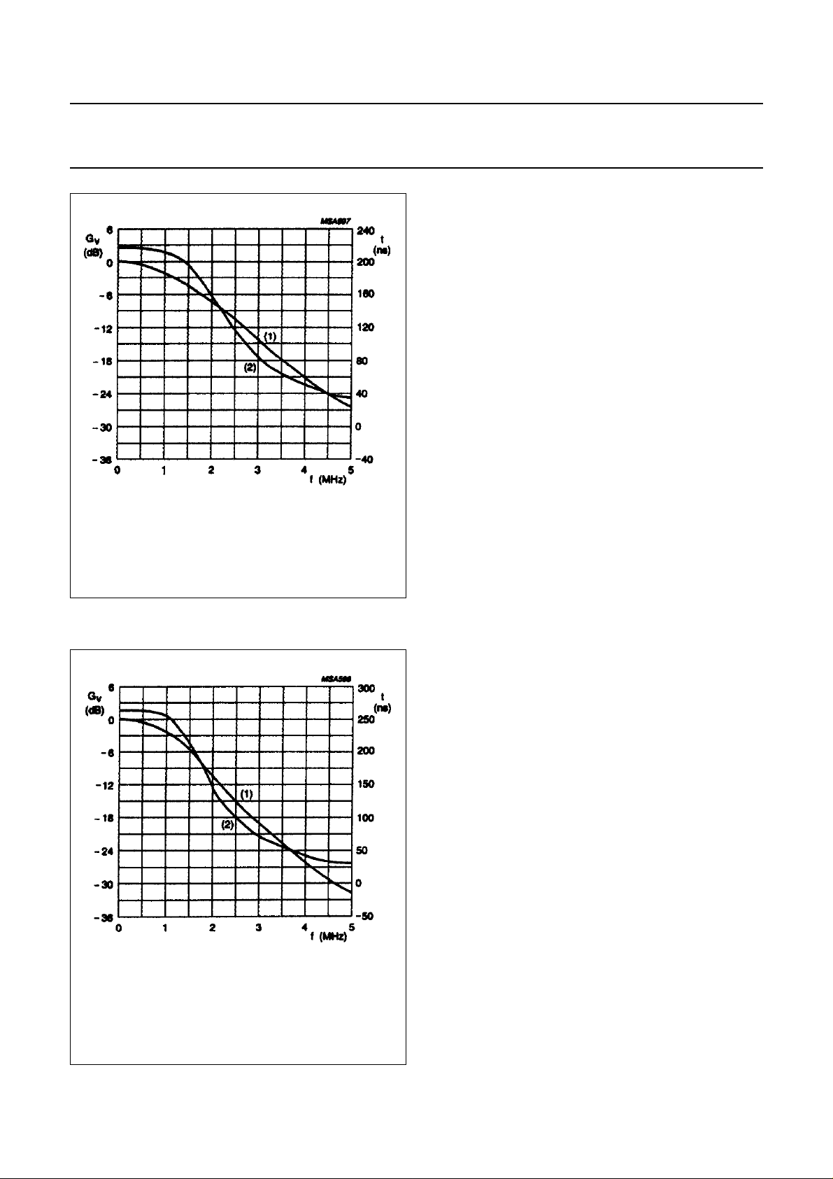
Low pass filters
The −3dB nominal frequency response level of the low
pass filters are different in PAL and NTSC modes.
PAL mode: bandwidth = 1.35 MHz nominal (see Fig.3).
NTSC mode: bandwidth = 1.1 MHz nominal (see Fig.4).
The signal outputs of the low pass filters are connected to
the signal inputs of the U and V modulators.
U
AND VMODULATORS
Two four-quadrant multipliers are used for quadrature
amplitude modulation of the U and V signals. The level of
harmonics produced by the modulated signals are
minimal, because of real multiplication with sinewave
carriers.
The unbalance of the modulators is minimized by means
(1) frequency response.
(2) group delay.
Fig.3 Low pass filter response for colour
difference signals (PAL mode).
of a control loop and two external capacitors, pin 6 for the
U modulator and pin 12 for the V modulator. The timing of
the control loop is triggered by the H/2 pulse, so that during
one sync period the U control is active and during the next
sync period the V control is active. In this way, when U and
V are both zero, the suppressed carrier is guaranteed to be
at a low level.
(1) frequency response.
(2) group delay.
Fig.4 Low pass filter response for colour
difference signals (NTSC mode).
The internal oscillator circuit generates two sinewave
carriers (0 degree and 90 degree). The '0 degree' (0)
carrier is connected to the U modulator and the '90 degree'
(1) carrier is connected to the V modulator.
PAL mode:
• switched sequentially by the H/2 pulse, the V signal is
modulated alternately with the direct and inverse carrier.
• the internal H/2 pulse can be forced into a specific phase
by means of an external pulse connected to pin 4 (H/2).
Forcing is active at HIGH level. If not used pin 4 can be
left open-circuit or connected to ground. If pin 4 is left
open, the internally generated H/2 pulse (output) is
connected to this pin.
NTSC mode:
• alternation of the V modulation is not allowed. If pin 4 is
not used for set-up control (see Y +SYNC, CVBS and
Chrominance outputs), it can be left open-circuit or
connected to ground.
April 1993 7
Philips Semiconductors Preliminary specification
PAL/NTSC encoder TDA8501
CHROMINANCE BLANKING
The signal outputs from the modulators are connected to
the signal input of the chrominance blanking circuit. To
avoid signal distortion that may be caused by the control
loop, the signal outputs of the modulators are blanked
during the sync period. This prevents signal distortion
during the adding of the sync pulse at the CVBS output
circuit.
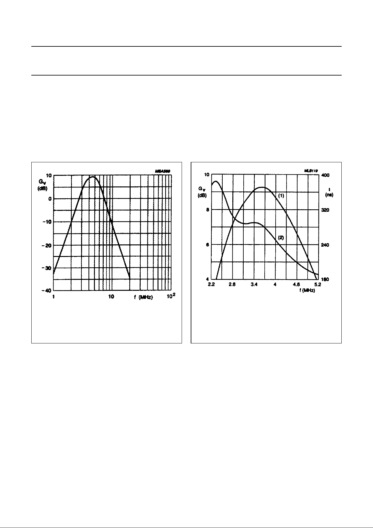
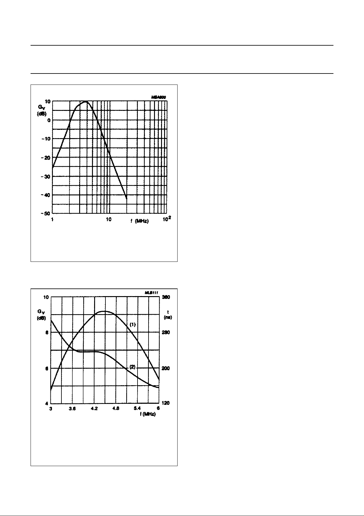
BANDPASS FILTER
A wide symmetrical bandpass filter is used so that a
maximum performance of the chrominance for Y +C
(SVHS) is guaranteed. This wide curve is possible
because of the minimal signal level of the harmonics within
the modulators see Figs (PAL mode: 5 and 6);
(NTSC mode: 7 and 8) which illustrate the nominal
response for PAL and NTSC modes.
Fig.5 Band pass filter nominal frequency
response (PAL mode).
(1) frequency response.
(2) group delay.
Fig.6 Band pass filter nominal frequency/group
delay response (PAL mode).
April 1993 8
Philips Semiconductors Preliminary specification
PAL/NTSC encoder TDA8501
Y +SYNC, CVBS AND CHROMINANCE OUTPUTS
The Y signal from the matrix, or the Y signal from pin 5,
(selected via the switch) is added with the composite sync
signal of the sync separator (dependent on pin 17
conditioning). The output of the adder, nominal 1 V
(peak-to-peak), is connected to pin 22 (see Fig.1). Pin 22
is connected to an external delay line.
The delay line is necessary for correct timing of the
Y + SYNC signal with the chrominance signal. The output
Fig.7 Band pass filter nominal frequency
response (NTSC mode).
resistor of the delay line is connected to V
output of the external delay line is connected to (input)
pin 20.
The Y +SYNC (delayed) input signal at pin 20 is amplified
via a buffer to a level of 2 V (peak-to-peak) nominal and
connected to pin 19 (Y + SYNC output).
The Y + SYNC (delayed) input signal at pin 20 is also
connected via an internal resistor of 2 kΩ to the input of the
CVBS adder stage. After the internal resistor of 2 kΩ, and
before the input of the CVBS adder, an external notch filter
can be connected via pin 18.
The chrominance output of the bandpass filter is added
with Y +SYNC signal via the CVBS adder. The CVBS
(combined video and blanking signal) output of the adder
is connected to pin 16 with a nominal amplitude of 2 V
(peak-to-peak).
(pin 13). The
REF
(1) frequency response.
(2) group delay.
Fig.8 Band pass filter nominal frequency/group
delay response (NTSC mode).
The chrominance output of the bandpass filter is amplified
via a buffer and connected to pin 14. The chrominance
amplitude corresponds with the value of Y + SYNC signal
output at pin 19. Together both outputs give the
Y +C (SVHS) signals.
B
LACK AND BLANKING LEVELS IN PAL AND NTSC MODES
PAL mode: Fig.9 illustrates the nominal Y + SYNC signal
at pin 22, the difference between black and blanking level
is 0 mV.
NTSC mode: Fig.10 illustrates the nominal Y + SYNC
signal at pin 22, the difference between black and blanking
level is 53 mV.
Because of the difference between the black and blanking
level in the NTSC mode, there are two options for NTSC.
April 1993 9
 Loading...