

Philips TDA8446, TDA8446T Datasheet

INTEGRATED CIRCUITS
DATA SH EET
TDA8446
Fast RGB/YC switch for digital
decoding
Product specification
Supersedes data of August 1992
File under Integrated Circuits, IC02
Philips Semiconductors
1995 Feb 16

Philips Semiconductors Product specification
Fast RGB/YC switch for digital decoding TDA8446
FEA TURES
• R, G, B clamped inputs
• Luminance and chrominance difference matrix
• Y-clamped inputs
• Fast switching between internal and external Y
• Chrominance input
• Amplifier with selectable gain
• 3-state switch for chrominance output.
APPLICATIONS
• Digital TV systems
• Desktop video architecture.
QUICK REFERENCE DATA
SYMBOL PARAMETER MIN. TYP. MAX. UNIT
V
CC
T
amb
ORDERING INFORMATION
supply voltage 10.8 − 13.2 V
operating ambient temperature 0 − +70 °C
DESCRIPTION
The TDA8446 is a video switch which has been designed
for use in Digital Multistandard System Decoders (DMSD)
in digital video system. The device is intended for matrixing
incoming RGB signals and for switching between
luminance signals. It generates a SYNC signal and TTL
clamping pulses from any video signal with sync pulses.
TYPE NUMBER
NAME DESCRIPTION VERSION
TDA8446 DIP20 plastic dual in-line package; 20 leads; (300 mil) SOT146-1
TDA8446T SO28 plastic small outline package; 28 leads; body width 7.5 mm SOT136-1
PACKAGE
1995 Feb 16 2
Philips Semiconductors Product specification
Fast RGB/YC switch for digital decoding TDA8446
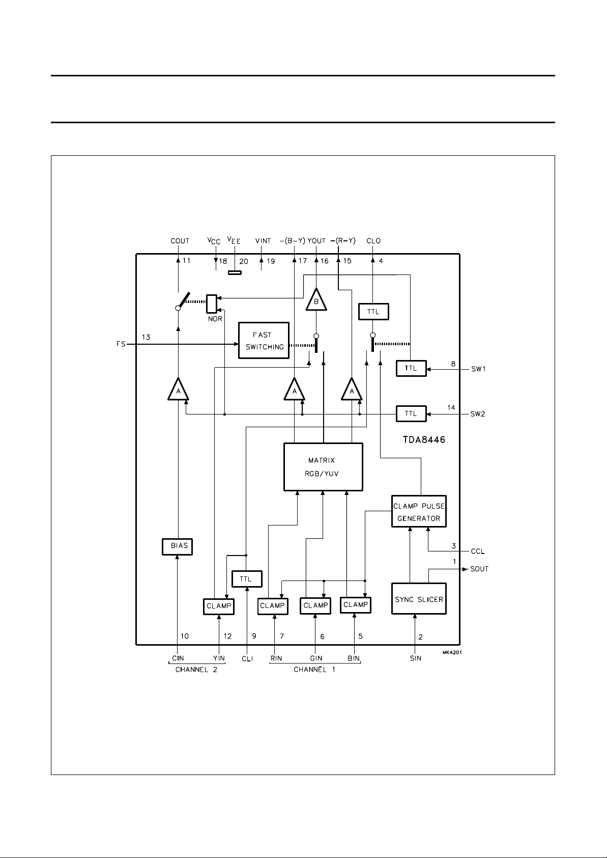
BLOCK DIAGRAM
Fig.1 Block diagram (TDA8446).
1995 Feb 16 3

Philips Semiconductors Product specification
Fast RGB/YC switch for digital decoding TDA8446
PINNING
SYMBOL
SOUT 1 1 synchronization signal output; this output provides the synchronization information
SIN 2 2 synchronization signal input; CSYNC or CVBS signal from the peri-connector
CCL 3 3 clamping capacitor connection; the clamping pulse is generated by external circuitry
n.c. − 4 not connected
CLO 4 5 clamping pulse output
n.c. − 6 not connected
BIN 5 7 B-signal input
GIN 6 8 G-signal input
RIN 7 9 R-signal input
SW1 8 10 clamping control signal input; this TTL signal is used to select the clamp signal, a LOW
n.c. − 11 not connected
CLI 9 12 clamping pulse input; this TTL signal indicates the black level clamping period for the
CIN 10 13 chrominance signal input
COUT 11 14 chrominance signal output
YIN 12 15 luminance signal input; this input also accepts the CVBS signal
FS 13 16 fast switching signal input; this signal is used to control fast switching of the luminance
n.c. − 17 not connected
n.c. − 18 not connected
SW2 14 19 gain control signal input; this TTL signal is used to set the gain of the chrominance
n.c. − 20 not connected
−(R-Y) 15 21 −(R−Y) signal output
YOUT 16 22 luminance signal output
−(B−Y) 17 23 −(B−Y) signal output
n.c. − 24 not connected
n.c. − 25 not connected
V
CC
VINT 19 27 internal decoupling
V
EE
PIN
DESCRIPTION
DIP20 SO28
extracted from the incoming signal at pin 2 (SIN).
connected to this pin, the generated pulse clamps the RGB inputs.
level at this input forces the circuit to output the generated clamping pulse.
incoming Y signal (active-HIGH).
signals, a HIGH level at this input forces the circuit to output the internal Y signal.
amplifiers (A), a LOW level at this input forces the gain A to 6 dB (HIGH forces to 0 dB).
18 26 positive supply voltage (+12 V)
20 28 ground
1995 Feb 16 4

Philips Semiconductors Product specification
Fast RGB/YC switch for digital decoding TDA8446
Fig.2 Pin configuration (DIP20). Fig.3 Pin configuration (SO28).
1995 Feb 16 5
 Loading...