

Philips TDA8444T-N4, TDA8444P-N4, TDA8444AT-N4 Datasheet
DATA SH EET
Product specification
Supersedes data of March 1991
File under Integrated Circuits, IC01
1999 Apr 29
INTEGRATED CIRCUITS
TDA8444; TDA8444T;
TDA8444AT
Octuple 6-bit DACs with I
2
C-bus
1999 Apr 29 2
Philips Semiconductors Product specification
Octuple 6-bit DACs with I2C-bus
TDA8444; TDA8444T;
TDA8444AT
FEATURES
• Eight DACs with 6-bit resolution
• Adjustable common output swing
• Push-pull outputs
• Outputs short-circuit protected
• Three programmable slave address bits
• Large supply voltage range
• Low temperature coefficient.
GENERAL DESCRIPTION
The interface circuit is a bipolar IC in a DIP16, SO16, or
SO20 package made in an I2L-compatible 18 V process.
The TDA8444 contains eight programmable 6-bit DAC
outputs, an I
2
C-bus slave receiver with three (two for
SO16) programmable address bits and one input (V
MAX
) to
set the maximum output voltage. Each DAC can be
programmed separately by a 6-bit word to 64 values, but
V
MAX
determines the maximum output voltage for all
DACs. The resolution will be approximately1⁄64V
MAX
.
At power-on all DACs are set to their lowest value.
QUICK REFERENCE DATA
ORDERING INFORMATION
SYMBOL PARAMETER CONDITIONS MIN. TYP. MAX. UNIT
V
CC
supply voltage 4.5 12 13.2 V
I
CC
supply current VCC=12V − 14 − mA
P power dissipation − 170 − mW
V
VMAX
input effective voltage 1 − VCC− 2.0 V
V
o(DACn)
DAC output voltage V
MAX=VCC
0.1 − VCC− 0.5 V
V
o(DACn)(max)
maximum DAC output voltage 1 < V
MAX<VCC
− 2.0 − V
MAX
+ 0.3 − V
I
source(min)
minimum DAC source current data = 1FH 2 −−mA
I
sink(min)
minimum DAC sink current data = 1FH 2 −−mA
TYPE
NUMBER
PACKAGE
NAME DESCRIPTION VERSION
TDA8444 DIP16 plastic dual in-line package; 16 leads (300 mil); long body SOT38-1
TDA8444T SO16 plastic small outline package; 16 leads; body width 7.5 mm SOT162-1
TDA8444AT SO20 plastic small outline package; 20 leads; body width 7.5 mm SOT163-1
1999 Apr 29 3
Philips Semiconductors Product specification
Octuple 6-bit DACs with I2C-bus
TDA8444; TDA8444T;
TDA8444AT
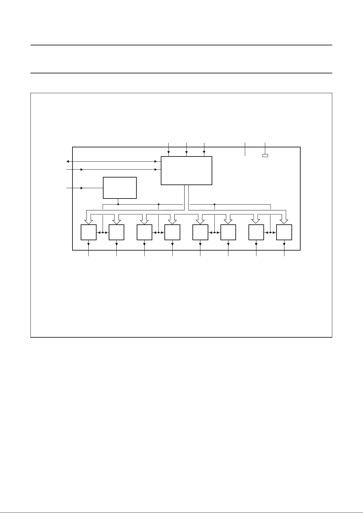
BLOCK DIAGRAM
Fig.1 Block diagram.
handbook, full pagewidth
MGH513
REFERENCE
VOLTAGE
GENERATOR
DAC0
DAC0
9
DAC1
DAC1
10
DAC2
DAC2
11
DAC3
DAC3
12
DAC4
DAC4
13
DAC5
DAC5
14
DAC6
DAC6
15
DAC7
DAC7
16
A0 A1 A2
567
18
SDA
SCL
3
4
V
MAX
2
V
CC
V
EE
TDA8444
I2C BUS
SLAVE RECEIVER
1999 Apr 29 4
Philips Semiconductors Product specification
Octuple 6-bit DACs with I2C-bus
TDA8444; TDA8444T;
TDA8444AT
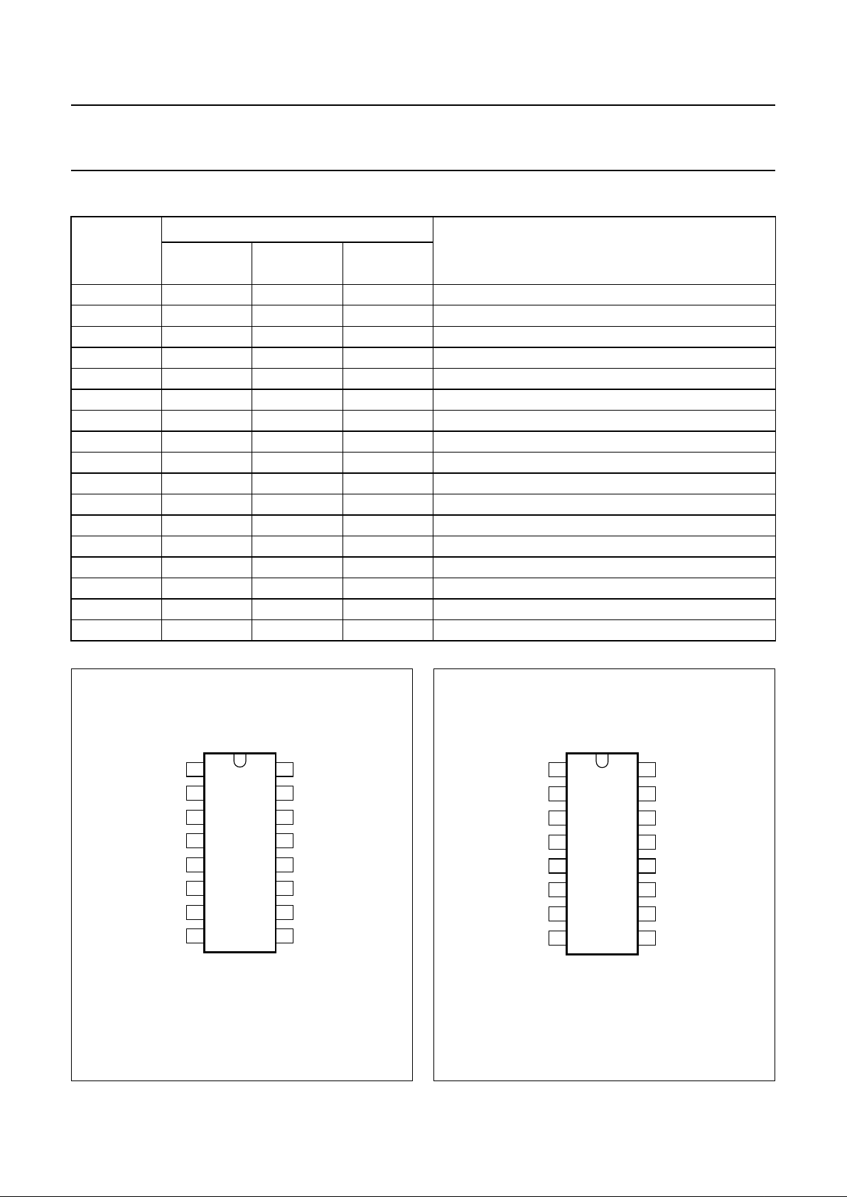
PINNING
SYMBOL
PIN
DESCRIPTION
TDA8444
(DIP16)
TDA8444T
(SO16)
TDA8444AT
(SO20)
V
CC
1 1 1 supply voltage
V
MAX
2 2 2 control input for DAC maximum output voltage
SDA 3 3 3 I
2
C-bus serial data input/output
SCL 4 4 4 I
2
C-bus serial clock
A0 5 6 7 programmable address bit 0 for I
2
C-bus slave receiver
A1 6 7 8 programmable address bit 1 for I
2
C-bus slave receiver
A2 7 − 9 programmable address bit 2 for I
2
C-bus slave receiver
V
EE
8 8 10 ground
DAC0 9 9 11 analog voltage output 0
DAC1 10 10 13 analog voltage output 1
DAC2 11 11 14 analog voltage output 2
DAC3 12 12 15 analog voltage output 3
DAC4 13 13 16 analog voltage output 4
DAC5 14 14 17 analog voltage output 5
DAC6 15 15 18 analog voltage output 6
DAC7 16 16 20 analog voltage output 7
n.c. − 5 5, 6, 12, 19 not connected
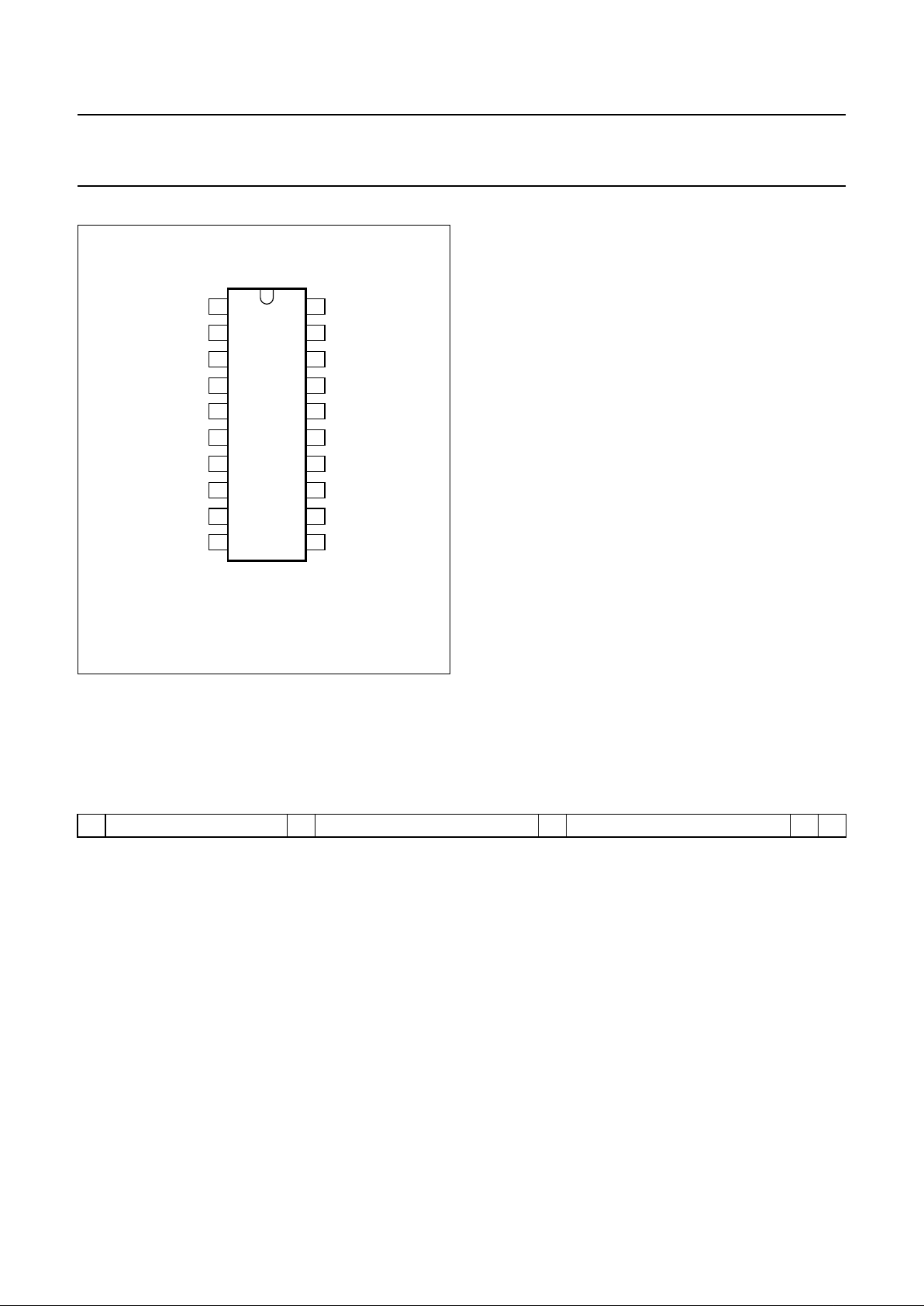
Fig.2 Pin configuration (TDA8444; DIP16).
handbook, halfpage
TDA8444
MGH512
1
2
3
4
5
6
7
8
16
15
14
13
12
11
10
9
V
EE
DAC0
A2 DAC1
A1 DAC2
DAC3
DAC4
DAC5
DAC6
DAC7
A0
SCL
SDA
V
MAX
V
CC
Fig.3 Pin configuration (TDA8444T; SO16).
handbook, halfpage
TDA8444T
MGL531
1
2
3
4
5
6
7
8
16
15
14
13
12
11
10
9
V
EE
DAC0
A1 DAC1
A0 DAC2
DAC3
DAC4
DAC5
DAC6
DAC7
n.c.
SCL
SDA
V
MAX
V
CC
1999 Apr 29 5
Philips Semiconductors Product specification
Octuple 6-bit DACs with I2C-bus
TDA8444; TDA8444T;
TDA8444AT
Fig.4 Pin configuration (TDA8444AT; SO20).
handbook, halfpage
TDA8444AT
MGL532
1
2
3
4
5
6
7
8
9
10
V
CC
V
MAX
SDA
SCL
n.c.
n.c.
A0
A1
A2
V
EE
DAC7
n.c.
DAC6
DAC5
DAC4
DAC3
DAC2
DAC1
n.c.
DAC0
20
19
18
17
16
15
14
13
12
11
FUNCTIONAL DESCRIPTION
I
2
C-bus interface
The I2C-bus interface is a receive-only slave, which accepts data according the format shown in Table 1.
Table 1 I
2
C-bus format (see note 1)
Note
1. S = START condition; A2 to A0 = programmable address bits; A = Acknowledge; I3 to I0 = Instruction bits;
SD to SA = subaddress bits; X = don’t care; D5 to D0 = data bits; P = STOP condition.
Valid addresses are:
TDA8444 and TDA8444AT: 40H, 42H, 44H, 46H, 48H, 4AH, 4CH and 4EH
TDA8444T: 48H, 4AH, 4CH and 4EH (A2 is always logic 1).
All other addresses cannot be acknowledged by the circuit. The actual slave address depends on the programmable
address bits A2, A1 and A0. This way up to eight circuits can be used on one I
2
C-bus.
Valid instructions are: 00H to 0FH; F0H to FFH.
S 0 1 0 0 A2 A1 A0 0 A I3 I2 I1 I0 SD SC SB SA A X X D5 D4 D3 D2 D1 D0 A P
 Loading...