Philips TDA8444 Service Manual

INTEGRATED CIRCUITS
DATA SH EET
TDA8444
Octuple 6-bit DAC with I
Product specification
File under Integrated Circuits, IC01
2
C-bus
March 1991

Philips Semiconductors Product specification
Octuple 6-bit DAC with I2C-bus
GENERAL DESCRIPTION
The TDA8444 comprises eight digital-to-analogue
converters (DACs) each controlled via the two-wire
I2C-bus. The DACs are individually programmed using a
6-bit word to select an output from one of 64 voltage steps.
The maximum output voltage of all DACs is set by the input
V
and the resolution is approximately V
max
At power-on all DAC outputs are set to their lowest value.
The I2C-bus slave receiver has a 7-bit address of which 3
bits are programmable via pins A0, A1 and A2.
Features
• Eight discrete DACs
2
C-bus slave receiver
• I
• 16-pin DIL package.
QUICK REFERENCE DATA
PARAMETER CONDITIONS SYMBOL MIN. TYP. MAX. UNIT
Supply voltage V
Supply current no loads; V
all data = 00 I
Total power dissipation no loads; V
all data = 00 P
Effective range of
V
input VP= 12 V V
max
DAC output voltage
range V
Step value of 1 LSB V
max
I
O
/64.
max
= VP;
max
= VP;
max
= VP;
= −2 mA V
CC
P
tot
max
O
LSB
TDA8444
10.8 12.0 13.2 V
81215mA
− 150 − mW
1 − 10.5 V
0.1 − VP−0.5 V
70 160 250 mV
PACKAGE OUTLINE
16-lead DIL; plastic (SOT38); SOT38-1; 1996 July 23.
March 1991 2

Philips Semiconductors Product specification
Octuple 6-bit DAC with I2C-bus
TDA8444
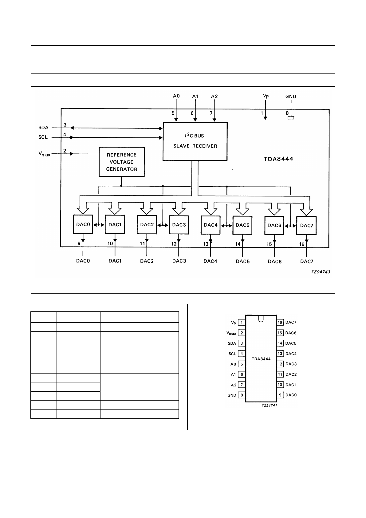
Fig.1 Block diagram.
PINNING
PIN SYMBOL DESCRIPTION
1V
2V
3 SDA I
4 SCL I
5A0
6A1
7A2
8 GND ground
9-16 DAC0-7 analogue voltage outputs
P
max
positive supply voltage
control input for DAC
maximum output voltage
2
C-bus serial data
input/output
2
C-bus serial data clock
programmable address bits
2
C-bus slave receiver
for I
Fig.2 Pinning diagram
March 1991 3
 Loading...