


DATA SH EET
Product specification
Supersedes data of November 1992
File under Integrated Circuits, IC02
1995 Mar 07
INTEGRATED CIRCUITS
Philips Semiconductors
TDA8443A
I
2
C-bus controlled YUV/RGB switch
1995 Mar 07 2
Philips Semiconductors Product specification
I2C-bus controlled YUV/RGB switch
TDA8443A
FEATURES
• Two RGB/YUV selectable clamped inputs with
associated synchronization
• RGB/YUV matrix
• 3-state switching with an OFF-state
• Selectable gain
• I2C-bus or non-I2C-bus mode
• Address selection for 7 devices
• Fast switching.
GENERAL DESCRIPTION
The TDA8443A is a general purpose two-channel switch
for YUV or RGB signals. One channel provides matrixing
from RGB to YUV, which can be bypassed.
The IC is controlled via I
2
C-bus by seven different
addresses or can be used in a non-I2C-bus mode. In the
non-I2C-bus mode, control of the circuit is achieved by DC
voltages.
QUICK REFERENCE DATA
ORDERING INFORMATION
SYMBOL PARAMETER CONDITIONS MIN. TYP. MAX. UNIT
V
P
supply voltage (pin 18) 10.8 12.0 13.2 V
I
P
supply current − 65 90 mA
RGB/YUV channels
Z
19-22
output impedance (pin 19) − 730Ω
Z
20-22
output impedance (pin 20) − 730Ω
Z
21-22
output impedance (pin 21) − 730Ω
B bandwidth −3 dB; mode 0 or 2 − 25 − MHz
+3 dB; mode 0 or 2 − 12 − MHz
±3 dB; mode 1 − 10 − MHz
V
O(p−p)
maximum output amplitude of YUV
signals (peak-to-peak value)
gain × 1 2.1 −−V
gain × 2 4.2 −−V
T
amb
operating ambient temperature 0 − +70 °C
TYPE
NUMBER
PACKAGE
NAME DESCRIPTION VERSION
TDA8443A DIP24 plastic dual in-line package; 24 leads (600 mil) SOT101-1

1995 Mar 07 3
Philips Semiconductors Product specification
I2C-bus controlled YUV/RGB switch
TDA8443A
BLOCK DIAGRAM
Fig.1 Block diagram.
handbook, full pagewidth
MLD003
A4 A3 A2 A1
I C-BUS INTERFACE/
DECODER
2
20 21 2319 22181716151413 24
B3 B2 B1
MATRIX
RGB/YUV
CLAMP CLAMP CLAMP
CLAMP PULSE
GENERATOR
CLAMP CLAMP CLAMP
2456710111289
TDA8443A
3 1
FAST
SWITCHING
SELfast
switching
SYNC2B/ (B Y)
input
internal
voltage
R/ (R Y)
input
G/Y
input
B/ (B Y)
input
SYNC1
ON
input
G/Y
input
R/ (R Y)
input
channel 1 channel 2
SDA SCL S0 S1 S2
V
GND
SYNC
output
clamp pulse
generator
R/ (R Y)
input
G/Y
input
B/ (B Y)
input
outputs
P

1995 Mar 07 4
Philips Semiconductors Product specification
I2C-bus controlled YUV/RGB switch
TDA8443A
PINNING
SYMBOL PIN DESCRIPTION
SEL 1 select input
(non-I
2
C-bus mode only)
SYNC2 2 synchronization input for
Channel 2
FS 3 fast switching input
R/±(R−Y)IN 4 R or (R−Y) signal input
G/Y IN 5 G or Y signal input
B/±(B−Y)IN 6 B or (B−Y) signal input
VINT 7 internal voltage supply
SYNC1 8 synchronization input for
Channel 1
ON 9 ON input
R/−(R−Y)IN 10 R or −(R−Y) signal input
G/Y IN 11 G or Y signal input
B/−(B−Y)IN 12 B or −(B−Y) signal input
SDA 13 serial data input/output; I
2
C-bus
SCL 14 serial clock input; I
2
C-bus
S0 15 address selection input 0
S1 16 address selection input 1
S2 17 address selection input 2
V
P
18 supply voltage
B/−(B−Y)OUT 19 B or −(B−Y) signal output
G/Y OUT 20 G or Y signal output
R/−(R−Y)OUT 21 R or −(R−Y) signal output
GND 22 ground
SYNC 23 synchronization output
CLAMP 24 clamping pulse generator
input/output
Fig.2 Pin configuration.
handbook, halfpage
TDA8443A
MLD004
1
2
3
4
5
6
7
8
9
10
11
12
24
23
22
21
20
19
18
17
16
15
14
13
SEL
SYNC2
FS
R/ (R Y) IN
G/Y IN
B/ (B Y) IN
V INT
SYNC1
ON
R/ (R Y) IN
G/Y IN
B/ (B Y) IN
CLAMP
SYNC
GND
R/ (R Y) OUT
G/Y OUT
B/ (B Y) OUT
V
S2
S1
S0
SCL
SDA
P
1995 Mar 07 5
Philips Semiconductors Product specification
I2C-bus controlled YUV/RGB switch
TDA8443A
FUNCTIONAL DESCRIPTION
The circuit contains two sets of inputs (see Fig.1). Both
channels can receive RGB or YUV signals. Each set of
inputs has its own synchronization input, which internally
generates a pulse to clamp the inputs. The internal
clamping pulse can also be controlled by a signal (e.g. a
sandcastle pulse) applied to pin 24. The pulse will occur
during the time that the signal at pin 24 is between
5.5 and 6.5 V. If both a sync signal and a pin 24 signal are
used the signal should be applied to pin 24 via a 1 kΩ
resistor.
RGB signals of Channel 2 can be matrixed to YUV signals.
The outputs can be set in a high impedance OFF state,
which allows the use of seven devices in parallel
(I
2
C-bus mode).
The circuit can be controlled by an I2C-bus compatible
microcontroller or directly by DC voltages. The fast
switching input can be operated via pin 16 of the
peritelevision connector.
I
2
C-bus mode
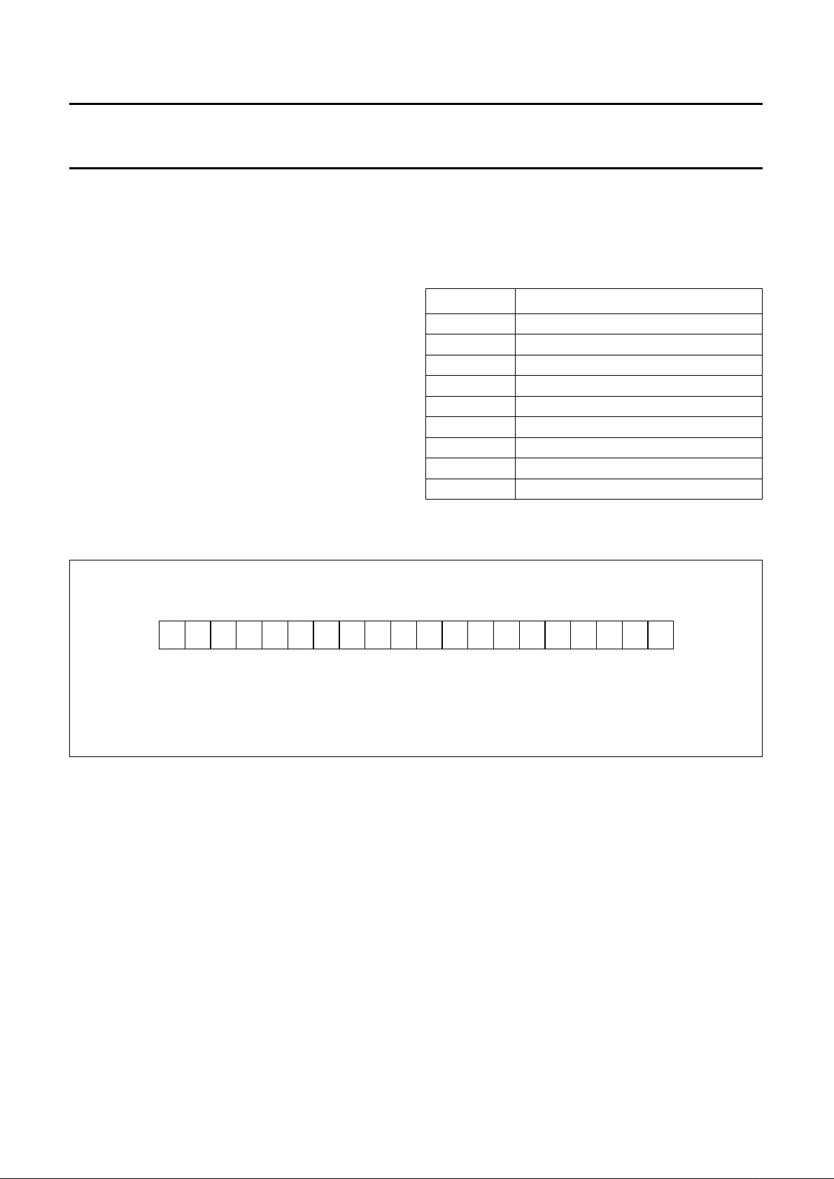
The protocol for the devices in I2C-bus mode is shown
in Fig.3.
Table 1 Protocol bit description
BIT DESCRIPTION
STA start condition
MA2 to MA0 address selection bits; see Table 2
ACK acknowledge bit
D7 channel selection bit; see Table3
D6 matrix selection bit; see Table3
D5 to D3 gain control bits; see Table 4
D2 fast switching priority bit; see Table5
D1 and D0 output state control bits; see Table 6
STO stop condition
Fig.3 I2C-bus protocol.
handbook, full pagewidth
STA 1 1 0 1 MA2 MA1 MA0 0 ACK D7 D6 D5 D4 D3 D2 D1 D0 ACK STO
MSA003
See Table1.

1995 Mar 07 6
Philips Semiconductors Product specification
I2C-bus controlled YUV/RGB switch
TDA8443A
Table 2 Address selection
Notes
1. L = LOW level input voltage.
2. H = HIGH level input voltage.
3. ∗ = non-I
2
C-bus operation.
Table 3 Mode control bits D7 and D6
Table 4 Gain setting (see also Table 9)
Matrix equations
The relationship between output and input signals of the matrix is as follows:
Y = 0.3R + 0.59G + 0.11B
R−Y = 0.7R − 0.59G − 0.11B
B−Y=−0.3R − 0.59G + 0.89B
ADDRESS SELECT PINS
(1)(2)
ADDRESS SELECT BITS
S2 (PIN 17) S1 (PIN 16) S0 (PIN 15) MA2 MA1 MA0
LLL∗
(3)
∗
(3)
∗
(3)
LLH001
LHL010
LHH011
HLL100
HLH101
HHL110
HHH111
MODE D7 D6 FUNCTION
0 0 0 Channel 2 selected, no matrix
1 0 1 Channel 2 selected, matrix active
2 1 0 Channel 1 selected
− 1 1 not allowed
D5 D4 D3 A1 A2, A3, A4 B1, B3 B2
00011−1 0.45
0011111
0 1 0 not allowed −−
01111−1 0.45
10022−1 0.45
1012111
1102211
11121−1 0.45
 Loading...