

Philips TDA8442 Datasheet

INTEGRATED CIRCUITS
DATA SH EET
TDA8442
2
I
C-bus interface for colour
decoders
Product specification
File under Integrated Circuits, IC01
March 1991
Philips Semiconductors Product specification
I2C-bus interface for colour decoders
GENERAL DESCRIPTION
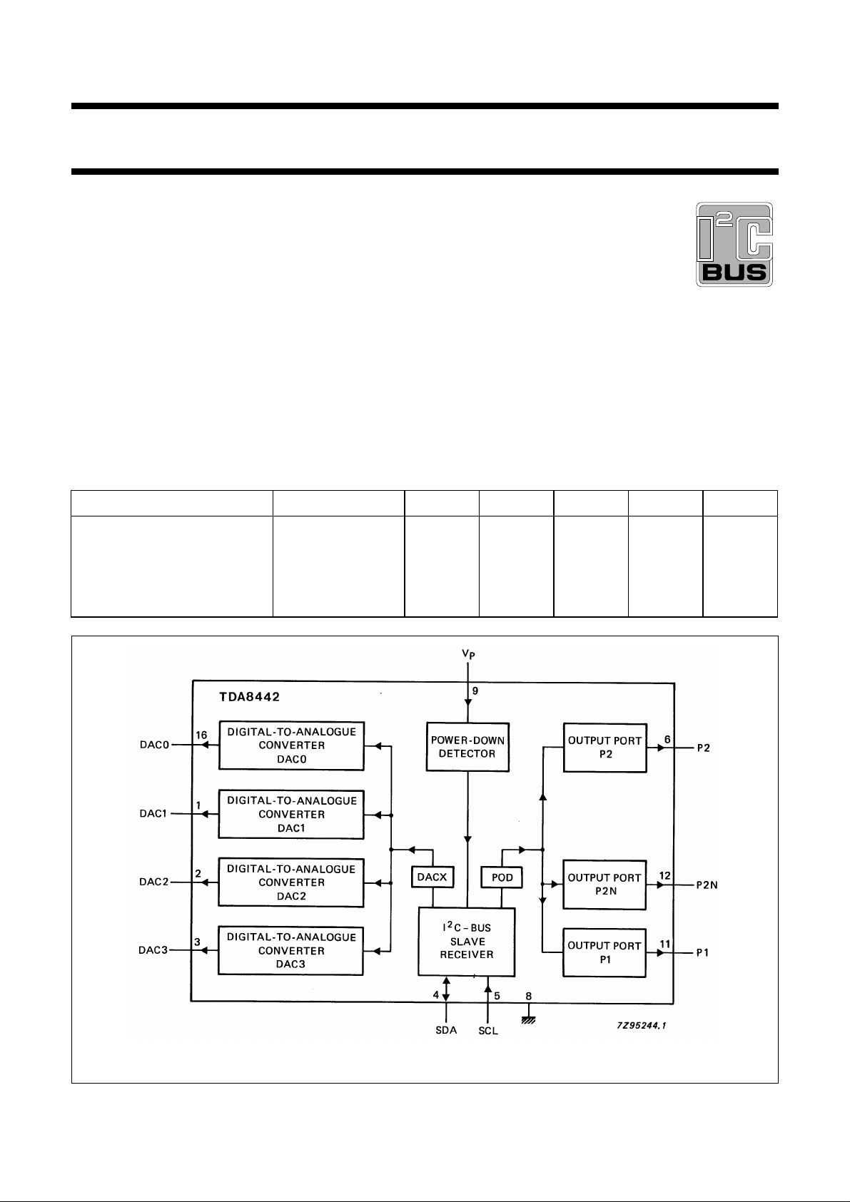
The TDA8442 provides control of four analogue functions
and has one high-current and two switching outputs.
Control of the IC is performed via the two-line, bidirectional
I2C-bus.
Features
• Four analogue control outputs
• One high-current output port (npn open emitter)
• Two switching output ports (npn collector with internal
pull-up resistor)
2
• I
C-bus slave receiver
• Power-down reset.
QUICK REFERENCE DATA
PARAMETER CONDITIONS SYMBOL MIN. TYP. MAX UNIT
Supply voltage (pin 9) V
Supply current no outputs loaded I
Total power dissipation no outputs loaded P
Operating ambient
temperature range
TDA8442
PACKAGE OUTLINE
16-lead DIL; plastic (SOT38); SOT38-1; 1996 July 23.
10.8 12.0 13.2 V
8 1318mA
−−1W
−20 −+70 °C
T
P
P
tot
amb
Fig.1 Block diagram.
March 1991 2
Philips Semiconductors Product specification
I2C-bus interface for colour decoders
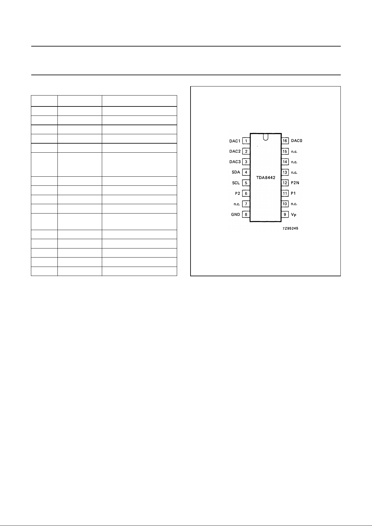
PINNING
PIN SYMBOL DESCRIPTION
1 DAC1 analogue output 1
2 DAC2 analogue output 2
3 DAC3 analogue output 3
4 SDA serial data line; I
5 SCL serial clock line; I
6 P2 Port 2 npn collector output
with internal pull-up
resistor
7 n.c. not connected
8 GND supply return (ground)
9V
10 n.c. not connected
11 P1 Port 1 open npn emitter
12 P2N inverted P2 output
13 n.c. not connected
14 n.c. not connected
15 n.c. not connected
16 DAC0 analogue output 0
P
positive supply voltage
output
2
C-bus
2
C-bus
TDA8442
Fig.2 Pinning diagram
FUNCTIONAL DESCRIPTION
Control
Analogue control is facilitated by four 6-bit digital-to-analogue converters (DAC0 to DAC3).
The values of the output voltages from the DACs are set via the I
The high-current output port (P1) is suitable for switching between internal and external RGB signals.
It is an open npn emitter output capable of sourcing 14 mA (min.).
The two output ports (P2 and P2N) can be used for NTSC/PAL switching. These are npn collector outputs with internal
pull-up resistors of 10 kΩ (typ.). Both outputs are capable of sinking up to 2 mA with a voltage drop of less than 400 mV.
If one output is switched on (LOW), the other output is switched off, and vice versa.
Reset
The power-down-reset mode occurs whenever the positive supply voltage falls below 8.5 V (typ.) and resets all registers
to a defined state.
2
C-bus.
March 1991 3
 Loading...