

Philips TDA8433 Datasheet

INTEGRATED CIRCUITS
DATA SH EET
TDA8433
Deflection processor for computer
controlled TV receivers
Product specification
File under Integrated Circuits, IC02
August 1991
Philips Semiconductors Product specification
Deflection processor for computer
TDA8433
controlled TV receivers
FEATURES
• I2C-bus interface
• Input for vertical sync
• Sawtooth generator with amplitude
independent of frequency
• Vertical deflection output stage
driver
• East-west raster correction drive
output
• EHT modulation input
• Changes picture width and height
without affecting geometry.
QUICK REFERENCE DATA
SYMBOL PARAMETER MIN. TYP. MAX. UNIT
V
CC
I
CC
V
2
V
21
supply voltage (pin 12) 10.8 12.0 13.2 V
supply current (pin 12) 12 20 27 mA
vertical sync trigger level − 3 − V
vertical feedback (note 1)
DC level −1.7 1.85 2.05 V
AC level 1.65 1.8 1.95 V
V
24
V
11-13
EHT compensation operating range 1.7 − 6V
inputs for control register data:
not locked to video − 0.7 1 V
at 50 Hz status 0.8 V
at 60 Hz status −−0.7 V
V
V
V
V
10-13
14-13
15
1
HCENT comparator switching level − V
SDA I2C-bus switching level data input − 3.5 − V
SCL I2C-bus switching level clock input − 3.5 − V
device selection where:
Ao = '1' 9.0 − V
Ao = '0' 0 − 2.0 V
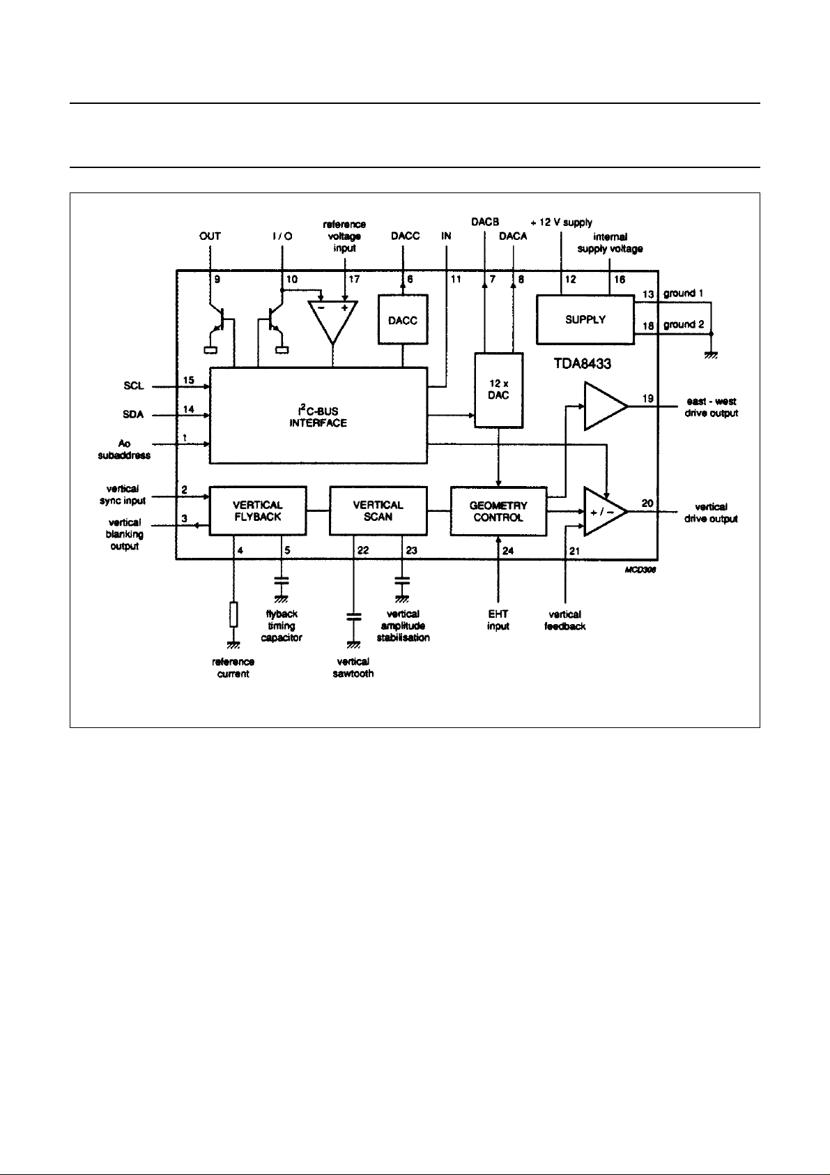
GENERAL DESCRIPTION
The TDA8433 is an I2C-bus
controlled deflection processor which,
together with a sync processor (e.g.
TDA2579A, see Fig.6), contains the
control and drive functions of the
deflection part in a computer
controlled TV receiver. The TDA8433
replaces all picture geometry settings
which were previously set manually
during manufacture.
CC
P
−−V
CC
17
− V
CC
V
V
Note to quick reference data
1. VR
= 0; V-S-corr = 0; V
in
= 20 H; V
shift
ampl
= 20 H.
ORDERING INFORMATION
PACKAGE
EXTENDED TYPE NUMBER
PINS PIN POSITION MATERIAL CODE
TDA8433 24 DIL plastic SOT101
Note
1. SOT101-1; 1996 December 2.
August 1991 2
(1)
Philips Semiconductors Product specification
Deflection processor for computer
controlled TV receivers
TDA8433
Fig.1 Block diagram.
August 1991 3
Philips Semiconductors Product specification
Deflection processor for computer
controlled TV receivers
PINNING
PIN DESCRIPTION
1 Ao subaddress
2 vertical sync input
3 vertical blanking output
4I
5 vertical blanking/flyback timing capacitor
6 DACC (tau switching)
7 DACB (horizontal phase)
8 DACA (horizontal frequency)
9 OUT (video switch)
10 I/O (f
11 IN (HLOCKN −50/60 Hz)
12 positive supply +12 V
13 ground 1
14 serial data input
15 serial clock input
16 internal supply voltage
17 voltage reference for I/O
18 ground 2 (waveform)
19 east-west drive output
20 vertical drive output
21 vertical feedback
22 vertical sawtooth capacitor
23 vertical amplitude capacitor
24 EHT input
resistor
ref
o
adjustment)
TDA8433
Fig.2 Pinning diagram.
August 1991 4

Philips Semiconductors Product specification
Deflection processor for computer
controlled TV receivers
PIN FUNCTIONS
Pin 1 - Ao subaddress
The Ao bit is the least significant bit
of the bus-address. It enables two
TDA8433s, with different
addresses, to be connected to the
same bus.
Pin 2 - Vertical sync input
Positive trigger pulses of > 3 V are
sufficient to exceed the internal
threshold of the ramp generator.
Flyback and blanking will then start
and, during the blanking period, the
circuit will be inhibited for further
input pulses (see Fig.3). It should be
noted that the TDA8433 has no
vertical oscillator therefore, the sync
processor, which is used in this
combination, has to provide trigger
pulses as well when the video input
is absent.
Pin 3 - Vertical blanking
The positive going blanking pulse is
fed from a current source. The
blanking period is fixed by the
capacitor connected to pin 5 and the
resistor connected to pin 4 (see
Fig.3).
Pins 4 and 5 - Reference/flyback
timing
The external resistor connected
between pin 4 and ground provides
a reference current for the triangle
generator circuit. This circuit
generates the triangle waveform at
pin 5. The width of the blanking
pulse is set by the external
capacitor connected to pin 5.
Table 1 Sync processor time constants
VTRA VTRC OUTPUT TIME CONSTANT
'0' '0' 12 V automatic operation
'0' '1' 5.3 V medium
'1' '0' 1.5 V fast (video recorder)
'1' '1' 0.2 V not to be used
Pin 6 - DACC (tau switching)
The output voltage, which depends
on the VTRA and VTRC bits in the
I2C-bus control register, is connected
to the coincidence detector of the
sync processor. In this way the time
constants of the horizontal PLL (in the
sync processor) can be set. If the
TDA2579 is used (see Fig.6) the
effect will be as listed in Table 1.
Pin 7 - DACB (horizontal phase)
The voltage at pin 7 is fed to the
horizontal pulse modulator in the sync
processor. This voltage, together with
the signal produced by the phase 2
detector during horizontal flyback,
sets the phase of the horizontal
output with respect to the flyback
pulse in the horizontal output stage.
The voltage range is variable
between 0.05 V and 10 V.
Pin 8 - DACA (horizontal
frequency)
The frequency of the horizontal
oscillator in the external sync
processor is adjusted by the voltage
level at pin 8. The voltage is variable
in 63 steps from 0.05 V to 10 V (i.e.
0.158 V per step).
Pin 9 - OUT (video switch)
The output at pin 9 is controlled by the
CVBS bit from the control register
where
CVBS = logic 0; the output is HIGH
(open collector)
TDA8433
CVBS = logic 1; the output is LOW
(saturation voltage)
An external video selector can be
controlled by means of this switching
function.
Pins 10 and 17 - I/O and Voltage
reference
Pin 10 is connected to the output of
the phase 1 detector in the sync
processor. Whether the pin is used as
an input or an output is dependent on
the PHI1 bit of the horizontal
frequency (HFREQ) register. When
PHI = logic 0 (output transistor open)
pin 10 is used as an input. The DC
information at this pin is compared
with the reference voltage at pin 17
and is reflected in the HCENT of the
status register.
HCENT = logic 0; input > V
HCENT = logic 1; input < V
In this way the free running frequency
can be adjusted by computer while
the oscillator is locked. Alternatively,
when PHI1 = logic 1, pin 10 is
switched to ground. The free running
frequency of the oscillator can the be
adjusted while watching the screen
provided that pin 10 is connected to
the video input of the sync processor.
Pin 11 -IN (HLOCKN and 50/60 Hz)
This pin is connected to the combined
MUTE and 50/60 Hz pin of the sync
processor. The various DC levels
define the state of the HLOCKN and
50/60 Hz bits in the status register
(see Table 2.)
ref
ref
at V
at V
17
17
August 1991 5

Philips Semiconductors Product specification
Deflection processor for computer
controlled TV receivers
Table 2 Status register bits
STATE OF SYNC PROCESSOR
(TDA2579)
Not locked to computer video < 0.7 V(min.) '1' '0'
60 Hz transmitter found 0.7 to 0.75 V
50 Hz transmitter found > 0.75 V
Pin 12 - Positive supply (12 V)
The nominal supply voltage at pin 12
is 12 V which should remain within
the defined limits. The nominal
current consumption is 20 mA.
Pins 13 and 18 - Ground (1 and 2)
Ground 1 (pin 13) is for the bus
transceiver section
Ground 2 (pin 18) is for the sawtooth
and picture geometry control section.
Pins 14 and 15 - SDA and SCL
(serial data and serial clock)
Input serial data is applied to pin 14.
The serial clock input from the
2
I
C-bus is applied to pin 15.
Pin 16 - Internal supply voltage
(+5 V)
In some applications it may be
necessary to connect a capacitor to
this pin to avoid interference.
Pin 19 - East-west drive output
The output drive for the East-west
correction circuit has a nominal range
from 1.6 to 11.7 V and contains 5
programmable parameters (see
Fig.5). The parameters are:
• Picture width
• East-west raster correction
• East-west trapezium correction
• East-west corner correction
• Compensation for EHT variations
TYPICAL VOLTAGE AT PIN 11
CC
to V
CC
CC
Pins 20 and 21 - Vertical drive
output and vertical feedback input
The vertical comparator and drive
output stage is designed so that the
feedback signal applied to pin 21 can
be inverted in the comparator by the
V-out control bit. This enables the use
of two different vertical output stages.
One output stage is without an
internal comparator (e.g. TDA3654).
The feedback signal at pin 21 has a
negative slope during scan. During
power-up the IC is adapted (preset)
for this type of output stage. The other
output stage contains a comparator.
The drive for this output stage is
obtained by interconnecting pins 20
and 21 and switching the V-out
polarity. The V-out bit will then be set
to logic 1. In both cases the drive
signal available at pin 20 contains 5
parameters which can be set via the
2
I
C-bus control;
• Picture height
• Vertical linearity
• Vertical S-correction
• Vertical shift
• Extent of compensation for EHT
variations (see Fig.4.)
Pins 22 and 23 - Vertical
sawtooth/vertical amplitude
capacitor
The 100 nF capacitor connected to
pin 22 is charged and discharged by
two current sources in the vertical
ramp generator. In order to obtain an
HLOCKN 50/60 Hz
'0' '0'
'0' '1'
equal amplitude, at different
frequencies, an amplitude
comparator has been incorporated.
The circuit, together with the 330 nF
capacitor connected to pin 23, keeps
the sawtooth amplitude at reference
voltage level (7.1 V). The external
load of the amplitude stabilization
loop of pin 23 should be as low as
possible. The recommended value is
≥ 500 MΩ.
Pin 24 - EHT input (Modulation)
A voltage between 1.7 and 6 V
(depending on the EHT variations)
applied to pin 24 will modulate the
amplitude of the vertical drive
sawtooth and the East-west drive
output. In this way the effect of beam
current variations can be virtually
eliminated.
2
I
C-BUS CONTROL
The addresses for the I2C-bus are
100011Ao0 (write) and 100011Ao1
(read). The inclusion of the Ao bit
makes it possible to control two
different deflection processors. After
receiving the address byte the
I2C-bus transmits its status byte in
which the status of the control bits is
contained.
PONRES - Power-on-reset
After switch-on, or a power dip below
6.7 V, the PONRES bit is set to logic
1. After a status read operation
PONRES is reset to logic 0.
STATE OF
TDA8433
August 1991 6

Philips Semiconductors Product specification
Deflection processor for computer
controlled TV receivers
HLOCKN - Horizontal lock
This bit indicates whether the
horizontal oscillator in the sync
processor is locked to the video
signal. When the oscillator is locked
HLOCKN is set to logic 0
(V11> 0.7 V). When the oscillator is
not locked HLOCKN is set to logic 1
(V11< 0.7 V).
HCENT - Horizontal centre
This bit is set to logic 0 when the
horizontal oscillator frequency is too
> V
high (V
10
). The bit is set to logic
ref
Table 3 Registers
FUNCTION
H-frequency 00 PHI-X-6 01 00
H-phase 01 6 01 00
Picture height V
21/20
V-linearity 03 6 01 00
V-S correction 04 6 01 00
V-shift 05 6 01 00
V-compensation
V
= 1.7 V
24
Picture width 07 6 01 00
E-W parabola
(Reg: 07 = 0)
E-W corner
(Reg: 08 = 3F)
Trapezium
Reg: 07 = 00; 08 = 20H
H-compensation
Reg. 07 = 00; 08 = 0; 09 = 00
V
= 1.7 V
24
1 when the frequency is too low
V10< V
ref
).
IN - 50/60 Hz
The voltage at pin 11 also contains
the 50/60 Hz information where:
logic 0 = ≤ V
0.75 VCC(60 Hz or no
11
transmitter)
logic 1 = ≥ V110.75 VCC(50 Hz)
The sequence of data in the status
byte is: PONRES, HLOCKN,
50/60 Hz, 0 0 0 0.
SUB
ADDR
HEX
DATA
BITS
PRESET
VALUE
HEX
02 6 01 00
06 5 01 00
08 6 01 00
09 6 01 00
0A 6 01 00
0B 5 01 00
TDA8433
A write operation starts with address
byte 100011Ao0. The device is then
ready to receive the subaddress byte
e.g. trapezium (HEXOA) 00001010
followed by the data byte e.g. HEX20.
The DAC will then set the trapezium
correction signal into the selected
position (see Fig.5). If more data
bytes follow within one transmission
then, by means of an auto-increment,
the next highest subaddress will be
selected. Wrap-around occurs after
HEXOF.
SETT
HEX
3F
3F
3F
3F
3F
3F
1F
3F
3F
3F
3F
1F
MIN. TYP. MAX. UNIT
−
9.5
−
9.5
−
+15
0
13
0
15
+17
−17
tbf
−8
−
6.0
−
7.0
−
1.7
0.75
1.0
0
−
0.05100.2
11
0.05100.2
11
−19
+19
−
17
−
19
+19
−19
−22
−
1
21
1
−
+22
+22
0
−10−−12
1.6
6.6
0.07
7.5
0
2.2
1.25
1.9
tbf
10
2.4
7.2
0.1
8.5
tbf
2.8
−
−
−
−
V
V
V
V
%
%
%
%
%
%
%
%
−
%
V
V
V
V
V
V
V
V
%
%
August 1991 7
Philips Semiconductors Product specification
Deflection processor for computer
TDA8433
controlled TV receivers
FUNCTION
SUB
ADDR
HEX
DATA
BITS
Not used 0C/0E −− −−−−
Control 0F X-VOUT − 40 11.5 11.9 V
VTRA−VTRC − 50 5.0 5.3 5.6 V
CVBS−X−X−X − 60 1.2 1.5 1.8 V
PHI1 bit 00 1 − 80 −−0.4
Not used 10−EF
Test functions F0−FF
PRESET
VALUE
HEX
SETT
HEX
MIN. TYP. MAX. UNIT
CC
V
70 0 0.2 0.5 V
40 5.5 7.5 9.5 kΩ
50 2.4 3.3 4.2 kΩ
60 0.7 1.0 1.35 kΩ
70 − 50 −Ω
00 −−(VBS) V
08 −−0.4
V
(1 mA)
V
(−2 mA)
00 −−V
CC
V
Note to Table 3
1. tbf = value to be fixed.
LIMITING VALUES
In accordance with the Absolute Maximum System (IEC 134)
SYMBOL PARAMETER MIN. MAX. UNIT
V
I
P
T
T
CC
CC
tot
amb
stg
supply voltage 10.8 13.2 V
supply current 12 27 mA
total power dissipation − 360 mW
operating ambient temperature range −25 +75 °C
storage temperature range −55 +150 °C
THERMAL RESISTANCE
SYMBOL PARAMETER TYP. MAX. UNIT
R
th j-a
from junction to ambient in free air − 35 K/W
August 1991 8
 Loading...