

Philips tda8421 DATASHEETS

INTEGRATED CIRCUITS
DATA SH EET
TDA8421
Hi-fi stereo audio processor;
2
I
C bus
Product specification
File under Integrated Circuits, IC02
May 1988
Philips Semiconductors Product specification
Hi-fi stereo audio processor; I2C bus
GENERAL DESCRIPTION
The TDA8421 is a monolithic bipolar integrated stereo sound circuit with a loudspeaker channel (CH1) and a headphone
channel (CH2), digital controlled via the I2C bus, for application in hi-fi audio and television sound.
Features
• Input selector
• Mode selector
• Loudspeaker channel (CH1); with volume control, balance control and mute
• Headphone channel (CH2); with volume control, balance control and mute
• Pseudo stereo and spatial function
• Bass and treble control
• Electrostatic discharge protection diodes
TDA8421
QUICK REFERENCE DATA
PARAMETER SYMBOL MIN. TYP. MAX. UNIT
Supply voltage (pin 4) V
Input signal handling V
Input sensitivity
full power at the output stage V
Signal plus noise-to-noise ratio (S+N)/N − 90 − dB
Total harmonic distortion THD − 0,05 − %
Channel separation α−75 − dB
Volume control range CH1 G −62 − 16 dB
Treble control range G −12 − 12 dB
Bass control range G −12 − 15 dB
Volume control range CH2 G −62 − 0dB
PACKAGE OUTLINE
28-lead dual in-line; plastic (SOT117); SOT 117-1; 1996 november 19.
CC
I
i
7,5 12 14 V
2 −−V
− 200 − mV
May 1988 2
Philips Semiconductors Product specification
Hi-fi stereo audio processor; I2C bus
TDA8421
May 1988 3
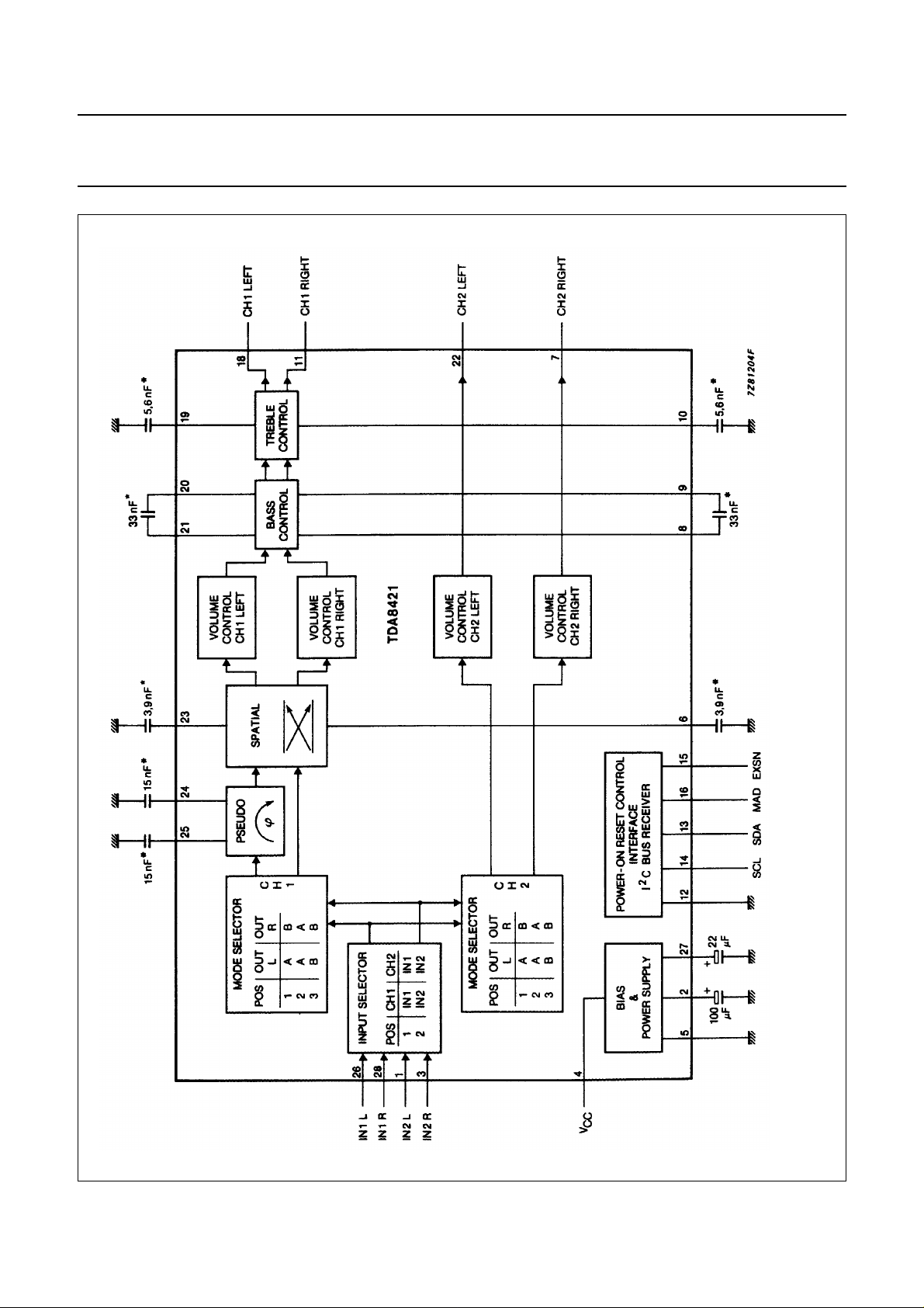
Fig.1 Block diagram.
* These values are dependent on the required frequency response and effect.

Philips Semiconductors Product specification
Hi-fi stereo audio processor; I2C bus
PINNING
TDA8421
Fig.2 Pinning diagram.
FUNCTIONAL DESCRIPTION
Input selector
The input to channel 1 (CH1) and channel 2 (CH2) is determined by the input selector. The selection is made from the
following AF input signals:
• IN1 L (pin 26); IN1 R (pin 28) or
• IN2 L (pin 1); IN2 R (pin 3)
Where IN1 is an internal input signal and IN2 an external input signal.
Mode selector
For each channel (CH1 and CH2) there is a mode selector which selects between stereo, sound A and sound B in the
event of bilingual transmission. Both mode selectors can be controlled independently.
May 1988 4

Philips Semiconductors Product specification
Hi-fi stereo audio processor; I2C bus
Headphone channel (CH2)
Volume control and balance
The stages for volume control for CH2 consist of two parts
for left and right. In each part the gain can be adjusted
between 0 and −62 dB in steps of 2 dB. An additional step
allows an attenuation of ≥ 90 dB. Both parts can be
controlled independently over the whole range, which
allows the balance to be varied by controlling the volume
of left and right.
Loudspeaker channel (CH1)
Volume control and balance
The loudspeaker channel (CH1) also consists of two parts
for volume control (left and right). In each part the gain
can be adjusted between + 16 dB and −62 dB in steps of
2 dB. An additional step allows an attenuation of ≥ 90 dB.
Both parts can be controlled independently over the
whole range, which allows the balance to be varied by
controlling the volume of left and right.
Stereo/pseudo stereo/spatial stereo mode
It is possible to select three modes. Stereo, pseudo or
spatial stereo. The pseudo stereo mode receives mono
transmissions and the stereo and spatial stereo mode
receives stereo transmissions.
Bass control
The bass control stage can be switched from an
emphasis of 15 dB to an attenuation of 12 dB for low
frequencies in steps of 3 dB.
Treble control
TDA8421
Bias and power supply
The TDA8421 includes a bias and power supply stage,
which generates a voltage of
impedance and injector currents for the logic part.
Power-on reset
The on-chip power-on reset circuit sets the mute bit to
active, which mutes both the loudspeaker channel (CH1)
and the headphone channel (CH2). The muting can be
switched by transmission of the mute bit.
2
I
C bus receiver and data handling
Bus specification
The TDA8421 is controlled via the 2-wire I2C bus by a
microcomputer. The two wires (SDA - serial data, SCL serial clock) carry information between the devices
connected to the bus. Both SDA and SCL are bidirectional
lines, connected to a positive supply voltage via a pull up
resistor.
When the bus is free both lines are HIGH. The data on the
SDA line must be stable during the HIGH period of the
clock. The HIGH or LOW state of the data line can only
change when the clock signal on the SCL line is LOW.
The set up and hold times are specified in
AC CHARACTERISTICS.
A HIGH-to-LOW transition of the SDA line while SCL is
HIGH is defined as a start condition. A LOW-to-HIGH
transition of the SDA line while SCL is HIGH is defined as
a stop condition. The bus receiver will be reset by the
reception of a start condition. The bus is considered to be
busy after the start condition. The bus is considered to be
free again after a stop condition.
1
⁄2VCCwith a low output
The treble control stage can be switched from + 12 dB to
−12 dB in steps of 3 dB.
Fig.3 TDA8421 module address.
The module address is determined by pin 16. When connected to ground MAD = 0; when connected to V
Thus two TDA8421s can be selected within a system.
May 1988 5
Module address
Data transmission to the TDA8421 starts with the module
address MAD.
MAD = 1.
CC
Philips Semiconductors Product specification
Hi-fi stereo audio processor; I2C bus
Subaddress
After the module address byte a second byte is used to select the functions for both channels:
• CH1 - Volume left, volume right, bass, treble and switch functions
• CH2 - Volume left, volume right and switch functions
The subaddress SAD is stored within the TDA8421. Table 1 defines the coding of the second byte after the module
address MAD.
Table 1 Second byte after module address MAD
128 64 32 16 8 4 2 1
MSB
CH1
CH2
FUNCTION
volume left 0 0 0 0 0 0 0 0
volume right 0 0 0 0 0 0 0 1
bass 0 0 0 0 0 0 1 0
treble 0 0 0 0 0 0 1 1
switch functions 0 0 0 0 1 0 0 0
volume left 0 0 0 0 0 1 0 0
volume right 0 0 0 0 0 1 0 1
switch functions 0 0 0 0 1 1 0 0
76543210
subaddress SAD
TDA8421
LSB
Definition of 3rd byte
A third byte is used to transmit data to the TDA8421. Table 2 defines the coding of the third byte after module address
MAD and subaddress SAD.
Table 2 Third byte after module address MAD and subaddress SAD
MSB LSB
CH1
CH2
FUNCTION
volume left VL1 1 1 V05 V04 V03 V02 V01 V00
volume right VR1 1 1 V15 V14 V13 V12 V11 V10
bass BA 1 1 1 1 BA3 BA2 BA1 BA0
treble TR 1 1 1 1 TR3 TR2 TR1 TR0
switch functions S1 1 1 MU EFL STL ML1 ML0 IS
volume left VL2 1 1 V25 V24 V23 V22 V21 V20
volume right VR2 1 1 V35 V34 V33 V32 V31 V30
switch functions S2 1 1 1 1 EXS MH1 MH0 1
765 4 3 2 1 0
May 1988 6
Philips Semiconductors Product specification
Hi-fi stereo audio processor; I2C bus
Truth tables
Truth tables for the switch functions
Table 3 Input selector
function IS
IN1 0
IN2 1
Table 5 Stereo/pseudo stereo/spatial stereo
choise STL EFL
spatial 1 1
stereo 1 0
pseudo 0 1
----------- 0 0
TDA8421
Table 4 Mode selectors
CH1 CH2
mode
stereo 1 1 1 1
sound A 1 0 1 0
sound B 0 1 0 1
---------- 0 0 0 0
Table 6 Mute
active; automatic
after POR
not active 0
Notes
1. Attenuation ≥ 90 dB; POR = Power-On Reset.
(1)
ML0 ML1 MH0 MH1
mute MU
1
Table 7 Output for external switch
EXSN EXS
ground 1
open collector 0
Truth tables for the volume base and treble controls.
Table 8 Volume control
CH1 CH2 V × 5V×4V×3V×2V×1V×0
160111111
14 −2 ⋅⋅⋅⋅⋅⋅
⋅⋅⋅⋅⋅⋅⋅⋅
⋅⋅⋅⋅⋅⋅⋅⋅
⋅⋅⋅⋅⋅⋅⋅⋅
−46 −62100000
−48 ≤−90011111
⋅⋅⋅⋅⋅⋅⋅⋅
−62 ≤−90011000
≤−90 ≤−90010111
⋅⋅⋅⋅⋅⋅⋅⋅
⋅⋅⋅⋅⋅⋅⋅⋅
⋅⋅⋅⋅⋅⋅⋅⋅
≤−90 ≤−90000000
Note
1. The values of CH1 and CH2 are in 2 dB/step measured in dBs.
May 1988 7
Philips Semiconductors Product specification
Hi-fi stereo audio processor; I2C bus
Table 9 Bass control
3dB/STEP
(dB)
15 1111
--- --- --- --- ---
--- --- --- --- ---
--- --- --- --- --15 1011
12 1010
--- --- --- --- ---
--- --- --- --- ---
--- --- --- --- --00110
--- --- --- --- ---
--- --- --- --- ---
--- --- --- --- ---
−12 0010
--- --- --- --- ---
--- --- --- --- ---
--- --- --- --- ---
−12 0000
BA3 BA2 BA1 BA0
TDA8421
Table 10 Treble control
3dB/STEP
(dB)
12 1111
--- --- --- --- ---
--- --- --- --- ---
--- --- --- --- ---
12 1010
--- --- --- --- ---
--- --- --- --- ---
--- --- --- --- --00110
--- --- --- --- ---
--- --- --- --- ---
--- --- --- --- ---
−12 0010
--- --- --- --- ---
--- --- --- --- ---
--- --- --- --- ---
−12 0000
TR3 TR2 TR1 TR0
May 1988 8
 Loading...