

Philips TDA8416 Datasheet

INTEGRATED CIRCUITS
DATA SH EET
TDA8416
TV and VTR stereo/dual sound
processor with integrated filters and
2
I
C-bus control
Preliminary specification
File under Integrated Circuits, IC02
November 1989

Philips Semiconductors Preliminary specification
TV and VTR stereo/dual sound processor with
integrated filters and I
GENERAL DESCRIPTION
The TDA8416 is a processor of stereo/dual language
signals (B/G-standard) for stereo sound television
receivers and VTRs, using the switched-capacitor
technique. The AF signals at the TDA8416 inputs must be
“(L+R)/2” or “language A” on one channel and “R” or
“language B” on the second channel (where L = left and
R = right). The carrier frequency of the second channel is
also modulated by an identification signal (stereo or dual
sound). The device is controlled by a microcomputer via
the two-line, bidirectional I2C-bus.
QUICK REFERENCE DATA
2
C-bus control
Features
• Use of the switched-capacitor technique for signal
processing
• Small amount of peripheral components
• Integrated anti-aliasing filters
• Low distortion AF signal handling
• Integrated de-emphasis with a time constant of 50 µs
• Two general purpose output ports
• Full ESD protection
TDA8416
PARAMETER CONDITION SYMBOL MIN. TYP. MAX. UNIT
Supply voltage (pin 15) V
Supply current (pin 15) I
AF output signal (RMS value)
(pins 11 to 14) V
Weighted signal-to-noise
ratio of the AF output
signals (CCIR 468/3) (S+W)/W 70 −−dB
Crosstalk attenuation
stereo mode at f = 1 kHz α
dual sound mode at f = 40 Hz to 12.5 kHz α
Pilot signal input sensitivity V
Total harmonic distortion THD − 0.1 − %
PACKAGE OUTLINE
20-lead DIL; plastic (SOT146); SOT146-1; 1996 November 18.
P
P
o
S
DS
i
− 12 − V
− 10 − mA
− 2 − V
40 −−dB
70 −−dB
− 2.5 − mV
November 1989 2
Philips Semiconductors Preliminary specification
TV and VTR stereo/dual sound processor
with integrated filters and I
2
C-bus control
TDA8416
November 1989 3
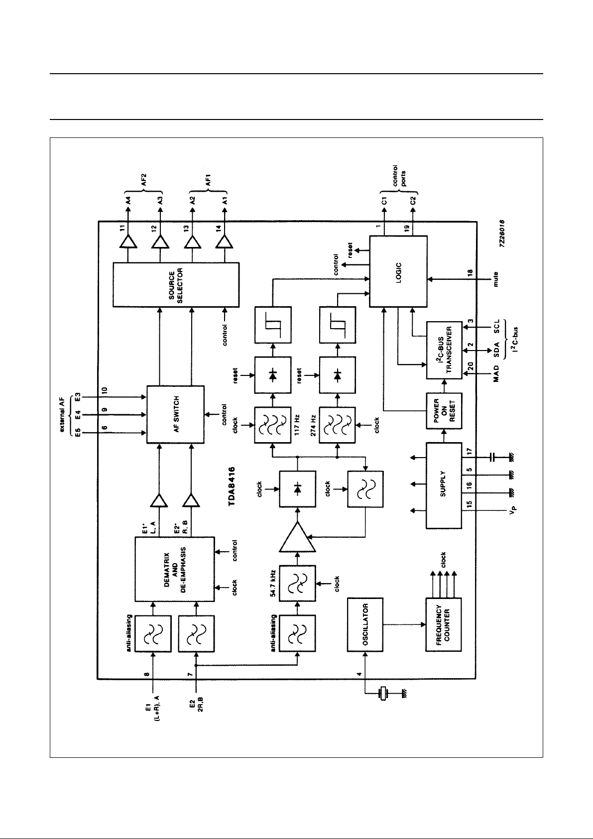
Fig.1 Block diagram.
Philips Semiconductors Preliminary specification
TV and VTR stereo/dual sound processor
with integrated filters and I
2
C-bus control
TDA8416
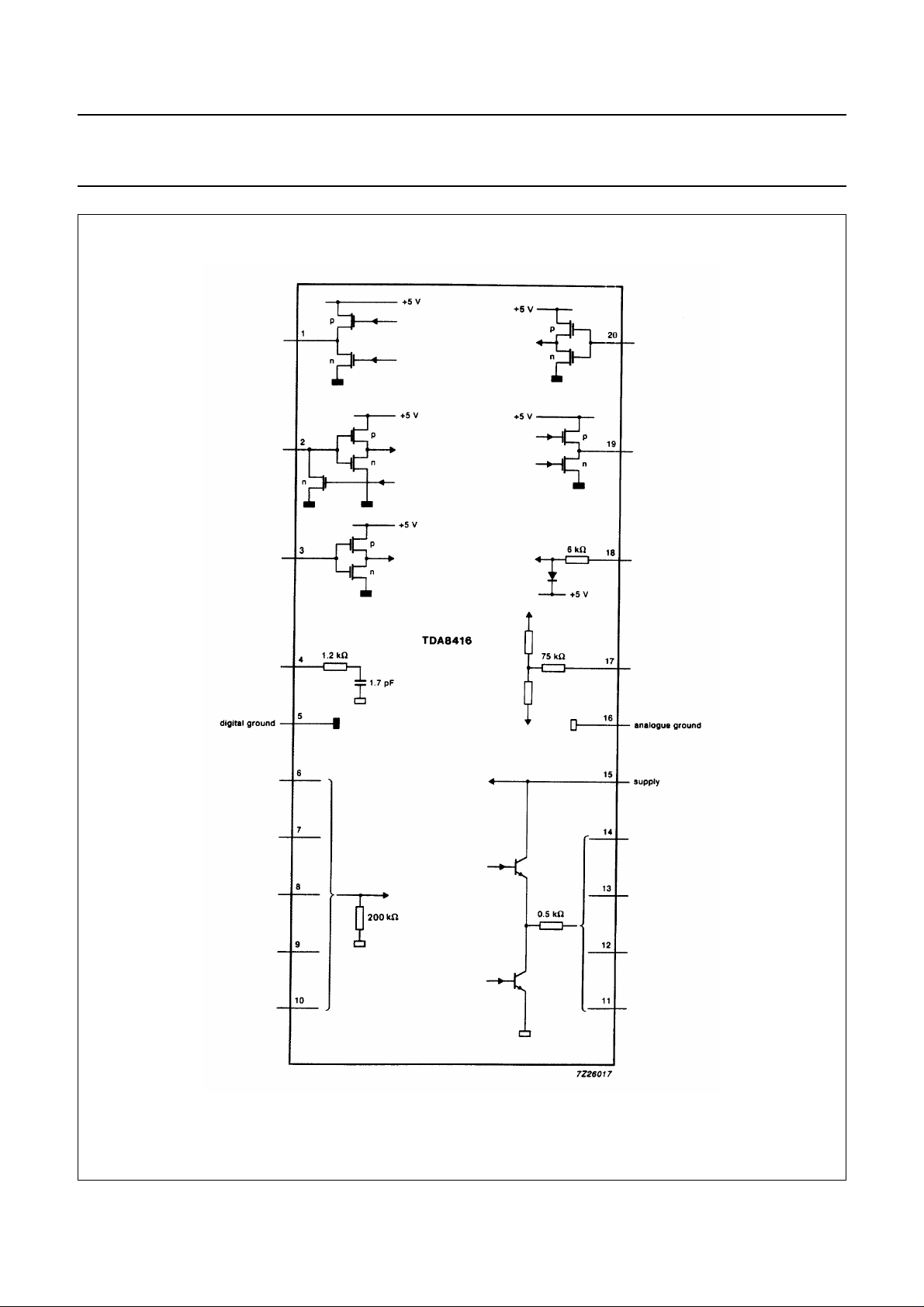
Fig.2 Input and output loading diagram.
November 1989 4

Philips Semiconductors Preliminary specification
TV and VTR stereo/dual sound processor
with integrated filters and I
PINNING
1 Control port C1
2
2 SDA, serial data line (I
3 SCL, serial clock line (I
4 Oscillator input (or quartz)
5 Digital ground (0 V)
6 External AF input (E5)
7 Sound channel input AF2 (E2)
8 Sound channel input AF1 (E1)
9 External AF input (E4)
10 External AF input (E3)
11 Output A4 AF 2 output
12 Output A3 AF 2 output
13 Output A2 AF 1 output
14 Output A1 AF 1 output
15 Supply voltage V
16 Analogue ground (0 V)
17 Ripple rejection improvement
18 Mute input
19 Control port C2
20 Module address (MAD)
C-bus)
2
C-bus)
P
2
C-bus control
TDA8416
FUNCTIONAL DESCRIPTION
Anti-aliasing filters
Frequency band limitation is performed by a second order Sallen and Key low-pass filter inserted in the AF signal path
and the identification circuit. This limitation is necessary because of the time-discrete signal processing needed to meet
the Nyquist criterium.
Identification
To enable the identification of the transmitted AF signal (mono, stereo or dual sound), the carrier frequency of the second
channel (E2) is also modulated by an identification signal. The identification signal is a 54.6875 kHz pilot carrier signal
which is 50% amplitude modulated by either a 117.4 Hz signal for stereo transmission or by a 274.1 Hz signal for dual
sound transmission.
The identification section of the circuit consists of a 54 kHz high-pass filter followed by a gain controlled amplifier with an
AM demodulator. The total gain of the high-pass filter and the amplifier is approximately 56 dB. The demodulated
identification signal is filtered by the identification band-pass filters, (117.4 Hz for stereo transmission, 274.1 Hz for dual
sound transmission). The output from either filter is converted to a DC signal by a peak detector and the necessary
hysteresis is performed by a Schmitt-trigger. The resultant DC output signals indicate the status of the transmitter (mono,
stereo or dual sound).
November 1989 5

Philips Semiconductors Preliminary specification
TV and VTR stereo/dual sound processor
with integrated filters and I
De-matrix and de-emphasis
Depending on the results of the identification circuit (mono, stereo or dual sound) the AF signals at the inputs E1 and E2
are converted to the signals at E1* and E2* as listed in Table 1.
Table 1 Transmitter status
TRANSMITTER STATUS E1 E2 E1* E2*
mono 0.7(L+R) − 2(L+R) −
stereo 0.7(L+R) 2R 4L 4R
dual sound 0.7A B 2A 2B
Note
1. L = left channel signal;
R = right channel signal;
A = first sound channel signal;
B = second sound channel signal
This section of the circuit also performs the de-emphasis (50 µs time constant) with a high degree of accuracy.
AF switch
(1)
2
C-bus control
TDA8416
The AF switch is used to switch to either the internal sound sources (E1* or E1* and E2*) or, to the external sound source
(E3 and E4) and is controlled via the I
Source selector
The source selector is used to connect the outputs from the AF switch to the outputs A1 to A4 as illustrated by Table 5.
The selector is controlled via the I
Muting
In this mode the AF outputs A1 to A4 are muted, and the identification circuit is deactivated (mono). The muting is active
after power-on reset or as a result of user control (via the mute input and bit CR3 of the control byte of the mute and port
control register; see Table 4).
Sound mute
If the switch register is set to (00) hex, (sound mute) only the AF outputs are muted, the identification circuit is still active
and can be read (status register) via the I2C-bus.
Power-on reset
The following actions are carried out by the internal power-on reset when it is active:
• The AF outputs are muted
• The identification circuit is deactivated (mono)
• The control ports (C1 and C2) are set LOW
2
• The I
C-bus transceiver is initialized
2
C-bus.
2
C-bus.
November 1989 6
 Loading...