

Philips TDA8385 Datasheet

INTEGRATED CIRCUITS
DATA SH EET
TDA8385
Control circuit for a Self-Oscillating
Power Supply (SOPS)
Preliminary specification
Supersedes data of September 1991
File under Integrated Circuits, IC02
Philips Semiconductors
March 1994

Philips Semiconductors Preliminary specification
Control circuit for a Self-Oscillating
Power Supply (SOPS)
FEATURES
• Bandgap reference generator
• Slow-start circuitry
• Low-loss peak current sensing
• Over-voltage protection
• Hysteresis controlled stand-by
function
• Error amplifier with gain setting
• Programmable transfer character
generator
• Protection against open- and
short-circuited feedback loop
ORDERING INFORMATION
EXTENDED TYPE
NUMBER
TDA8385 16 DIL plastic SOT38WBE
PINS PIN POSITION MATERIAL CODE
• Over-load current fold back
characteristic
• LED driver
• Demagnetization protection
• Programmable determination of
switch-on moment of switching
transistor for low-switching losses
• Feed-forward input
• Regulation-indicator output
• Programmable minimum on-time of
switching transistor
• Accurate peak-current setting.
TDA8385
GENERAL DESCRIPTION
The TDA8385 is intended to be used
in combination with the opto-coupler
(CNR50) as a control unit for a
self-oscillating power supply.
PACKAGE
March 1994 2

Philips Semiconductors Preliminary specification
Control circuit for a Self-Oscillating
Power Supply (SOPS)
BLOCK DIAGRAMS
handbook, full pagewidth
current reference
setting
feed forward
input
regulation indicator
output
differential amplifier
output
I
ref
3
V
fo
13
1 RIO
11Vdiff
REFERENCE
BLOCK
I
ref
REGULATION
INDICATOR
V
DIFFERENTIAL AMPLIFIER
TDA8385
V
P GND
16 14
latch
V
diff
V
P (min)
DETECTOR
7
V
reset
2812
(28, 27, 23)
mv
V
ts
I
STABILIZED
SUPPLY
V
ref
29
stab
SUPPLY REFERENCES
V
ts
X
V
ref
(2.5 V)
3
feedback voltage
input
transistor-on
setting input
slow start voltage
input
V
9
T
on(min)
4
7Vss
fb
50 µA
5
CLAMP
TCG
2.5 V
4
+
T
V
on (min)
ss
reset (28)
quick
discharge
Fig.1 Block diagram; part A (continued in Fig.2; part B).
V
TCG
CONTROL PART
27
SLOW START
MINIMUM
VOLTAGE
CLAMP
50 µA
charge
19
6
III
VII
MCD417
March 1994 3
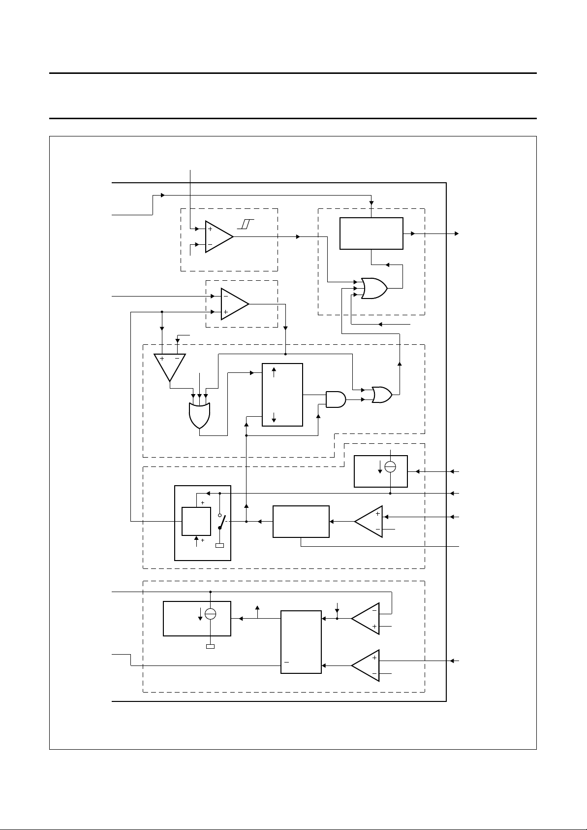
Philips Semiconductors Preliminary specification
Control circuit for a Self-Oscillating
Power Supply (SOPS)
handbook, full pagewidth
stand-by voltage input
V
10
sb
latch
2.5 V
V
r
V
sim
(28)18
2.5 V
25
STAND-BY
8
2 V
PWM
IV
S
IX
comparator
latch
OUTPUT
STAGE
17
LED DRIVER
TDA8385
LED
15
VI
Q (23)
2
TDA8385
LED driver output
26
demagnetization
100 mV
100 µA
slow
discharge
OVER-VOLTAGE PROTECTION
10
(17) (28)
21
FF
Q
R
13
V
c
DELAY
12
SAWTOOTH GENERATOR
QR
FF
23
S
Q
16
demagnetization
LED CONTROL
I
sim
0.2 I
11
24
22
14
12
I
I
12
9
peak
DEM
115 mV
II
115 mV
over voltage
2.5 V
VIII
V
12
current simulation
input
5
peak-current
setting input
15
demagnetization
input
6
delay setting
8
over-voltage
protection
Fig.2 Block diagram; part B (continued from Fig.1; part A).
March 1994 4
MCD418
Philips Semiconductors Preliminary specification
Control circuit for a Self-Oscillating
Power Supply (SOPS)
PINNING
SYMBOL PIN DESCRIPTION
RIO 1 regulation indicator output
LED 2 LED driver output
I
ref
T
on(min)
I
peak
DELAY 6 delay setting
V
ss
OVP 8 over-voltage protection
V
fb
V
sb
V
diff
I
sim
V
fo
GND 14 ground (0 V)
DEM 15 demagnetization input
V
P
3 current reference setting
4 transistor-on setting input
5 peak current setting input
7 slow start voltage input
9 feedback voltage input
10 stand-by voltage input
11 differential amplifier output
12 current simulation input
13 feed forward input
16 positive supply voltage
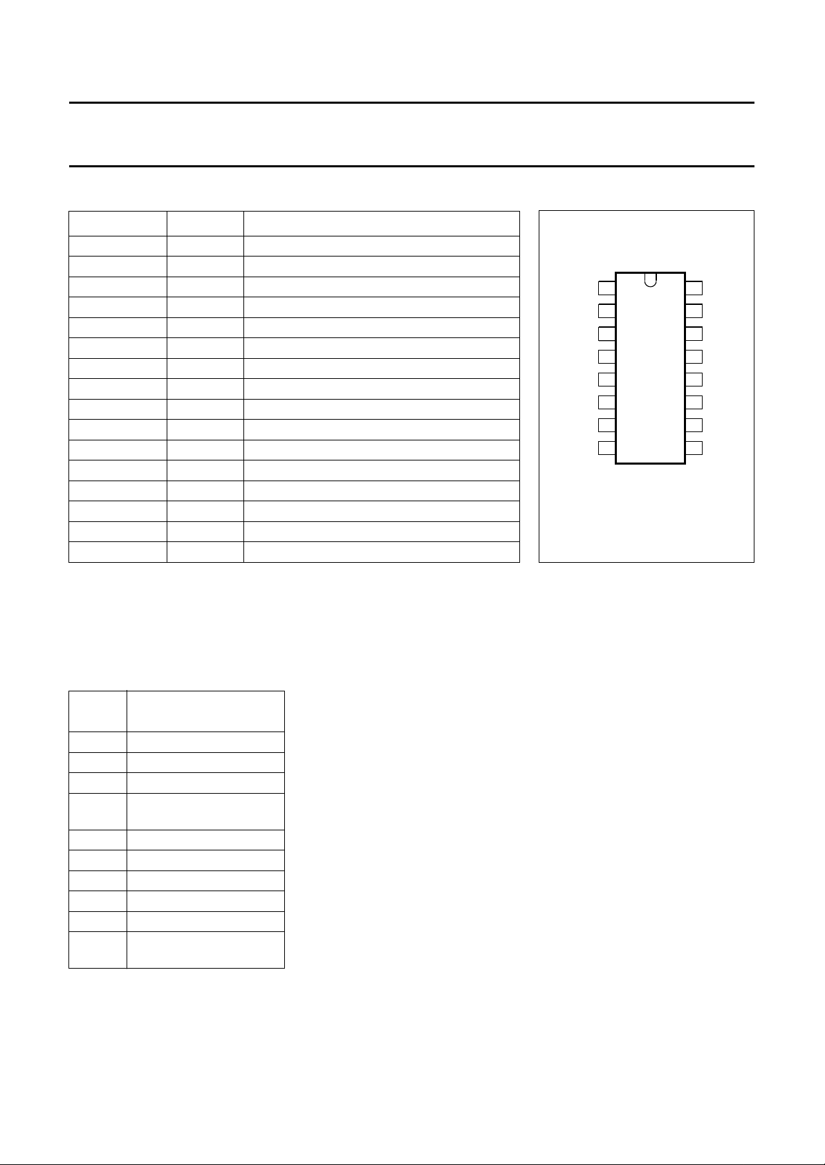
handbook, 2 columns
T
on(min)
DELAY
I
peak
OVP
RIO
LED
I
V
ref
1
2
3
4
5
6
7
ss
8
Fig.3 Pinning diagram.
TDA8385
TDA8385
MCD402
V
16
P
DEM
15
GND
14
V
13
fo
I
12
sim
V
11
diff
V
10
sb
V
9
fb
FUNCTIONAL DESCRIPTION
The TDA8385 can be divided into
10 functional blocks as shown in Fig.1
and Fig.2.
Block for Figs 1 and 2
BLOCK
NO.
DESCRIPTION
I supply references
II sawtooth generator
III control part
IV pulse width modulator
(PWM)
V LED control
VI LED driver
VII slow-start circuitry
VIII over-voltage protection
IX stand-by circuit
X regulation-indicator
output
These 10 functional blocks of Fig.1
and Fig.2 contain sub-sections
numbered 1 to 28 which are
cross-referenced in the following
description.
Supply references (Block I)
The TDA8385 is intended to be used
on the secondary side of the
self-oscillating power supply. It can be
supplied either by an auxiliary winding
of the transformer or an external
supply e.g. 50 Hz transformer.
Charging of the capacitor C
(see
P
Fig.16) takes place during transistor
on-time (Ton; see Fig.17). During
stand-by the IC is supplied by the
stand-by voltage Vsb (pin 10). The
operating voltage range is from 7.5 to
20 V. The supply current, inclusive
drive current for the LED, is less than
20 mA. A bandgap based reference
(2.5 V) generates a stabilized voltage
V
of 3.9 V to supply all internal
stab
circuits of the IC except the LED
driver. The LED driver is directly
supplied by VP. The reference block
generates all the reference voltages
in the circuit. By means of a resistor
connected to pin 3, a reference
current (I
) is defined.
ref
This current is reflected several times
and is used to obtain IC-independent
settings e.g. T
setting, delay
on(min)
setting, charging and discharging of
slow-start capacitor Css on pin 7
(see Fig.16).
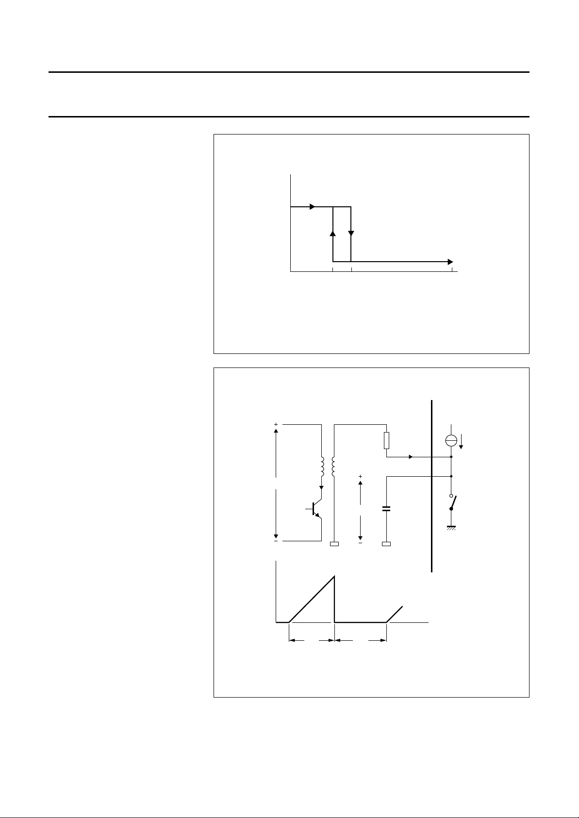
The power supply is released by the
opto-coupler IC at an input voltage
level, which is high enough to
guarantee correct operation of the
TDA8385 e.g. VP = 10 V by sensing
the mains voltage VI. As soon as the
SOPS switching transistor (T1, see
Fig.16) is conductive the capacitor C
is charged. As long as the IC supply
voltage is below 7.5 V the LED driver
is blocked (see latch output;
sub-section 28) in order to guarantee
start-up of SOPS.
During the initialization phase the
quick-discharge-switch
(sub-section 27), set input of
flip-flop (13) and reset input of
flip-flop (23) are also activated.
As soon as the voltage of 7.5 V is
reached the control functions of the IC
are operative. Hysteresis on the
initialization level is 2.3 V.
P
March 1994 5
Philips Semiconductors Preliminary specification
Control circuit for a Self-Oscillating
Power Supply (SOPS)
Sawtooth generator (Block II)
URRENT SIMULATION
C
(SEE FIGS 5 AND 16)
The current of the power supply
switching transistor is detected on the
secondary side by an indirect method
of current sensing.
Information of the collector current (Ic)
is obtained by integrating the voltage
of an auxiliary winding of the
transformer during transistor on-time
(Ton). An external capacitor C on pin 5
is charged during Ton by the current
source I
reflection of the current which flows
into pin 12. This current is obtained by
connecting an external resistor R12 to
the auxiliary transformer winding.
During transistor on-time this current
is related to the input voltage VI.
During transistor off time (T
capacitor C is discharged by switch
sw1. This switch is active during the
total T
voltage Vc is formed across C. This
sawtooth is a measure for the
collector current of the switching
transistor T1.
For the voltage Vc yields:
V
c
. The current I
sim
time. In this way a sawtooth
off
I
×
simTon
=
------------------------ C
sim
is the
) the
off
(1)
TDA8385
latch
initialization
operation
5.2 7.5 20
Fig.4 Latch initialization as a function of supply voltage VP.
L
n
n
p
h
V
I
T1
I
c
V
c
R12
C
I
12
VP(V)
12
5
I
sw1
MCD403
sim
I
sim
---------- -
----- n
R12
p
×
p
Where: p = reflection factor;
I
sim
--------I
12
0.2==
p
(2)
V
c
V
n
h
I
×=
(2) → (1) gives:
V
n
p
h
V
c
×
----- -
--- C
n
× T
---------- R12
p
I
×=
on
(3)
March 1994 6
t
T
on
T
off
MCD404
Fig.5 Determination of the peak current Ic.

Philips Semiconductors Preliminary specification
Control circuit for a Self-Oscillating
Power Supply (SOPS)
For ‘Ton’ yields:
VcC× np× R12×
T
=
---------------------------------------------- -
on
pn
× V
×
h
I
For the primary current Ic yields:
V
I
T
I
×=
-----
c
on
L
Substitution (4) into (5):
C
I
--- -
c
L
n
1
p
×
× R12× V
-- -
----- -
p
n
h
×=
c
Equation (6) shows that by limiting the
voltage V
the collector peak current
c
can be limited. The peak current is
limited by means of the clamping
circuit in the transfer character
generator (TCG); see Fig.1
sub-section 4.
D
ELAY SETTING (PIN 6)
The output of sub-section 11 is
(4)
extended by the delay circuit of
sub-section 12. The starting
(reference) point of the delay circuit is
the falling edge of the output of
demagnetizing comparator (11) The
(5)
delay can be determined externally by
capacitor (C
The switch-on moment of the
switching transistor can be
(6)
determined by capacitor C
A minimum delay time is required to
prevent transistor T1 from switching
during demagnetization of the
transformer because of oscillations
caused by the leakage inductance.
delay
) on pin 6.
delay
TDA8385
Control part (Block III)
The differential amplifier,
sub-section 3, compares the
feedback voltage (Vfb) with the
reference voltage V
the differential amplifier is available
on pin 11 to allow gain setting. The
differential amplifier is internally
compensated for 0 dB feedback
stability.
The feedback input (pin 9) is also
.
used as the input for the TCG
(see Fig.6) with which a current
foldback characteristic can be
obtained as shown in Fig.7.
. The output of
ref
The clamping level can be externally
influenced by means of a resistor
on pin 7.
The collector peak current can be
influenced in several ways:
• Resistor R12 on pin 12
• Capacitor C on pin 5
• Capacitor on pin 7
• Transfer ratio nh/n
p
• Inductance L
Before comparing the sawtooth
voltage Vc with the control voltage V
in the pulse width modulator, a
voltage of 100 mV is added to Vc. In
this way it will be possible for Vr to
become smaller than V
, which is
sim
important for a stabilized no-load
operation (see Fig.6 area 3).
D
EMAGNETIZATION INPUT (PIN 15)
This input prevents the switching
transistor from conducting during
demagnetization of the transformer in
order to prevent the transformer from
going into saturation. The output of
comparator (11) is HIGH as soon as
the voltage of the transformer winding
exceeds 115 mV.
(3)
V
mv
(4)
(2)
r
(1)
(5)
V
fb
(1), (2), (3) = V
(4), (5) = V
.
TCG
.
diff
V
clamp
V
Ton(min)
MCD405
Fig.6 Reference voltage (Vmv) as a function of feedback voltage (Vfb).
March 1994 7
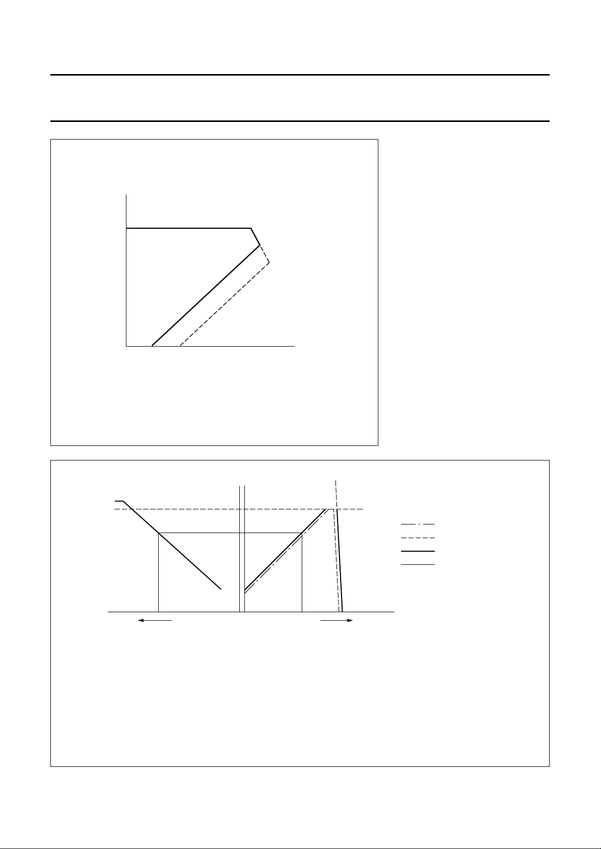
Philips Semiconductors Preliminary specification
Control circuit for a Self-Oscillating
Power Supply (SOPS)
V
O
(5)
(1)
(1), (2), (3) = V
(4), (5) = V
.
TCG
.
diff
Fig.7 Current foldback characteristic; stabilized output voltage (VO)
as function of load current (IO).
(4)
(2)
(3)
I
O
MCD406
TDA8385
The voltage V
minimum on-time of the switching
transistor. This voltage can be
determined externally with a resistor
on pin 4. With this resistor the current
foldback characteristic can be
influenced (see dotted line in Figs 6
and 7).
The minimum on-time is of
importance for the following.
• Stand-by operation
• Starting-up of power supply
• Overload and short-circuit
conditions.
The output of the differential amplifier
(V
), the output of the TCG (V
diff
and the voltage Vss + V
compared in a minimum voltage
clamping circuit (see Fig.1
sub-section 6). The output voltage is
equal to the lowest input voltage.
Some relevant characteristics of the
control part are depicted in Fig.8.
Ton(min)
determines the
TCG
are
Ton(min)
)
I
V
c
handbook, full pagewidth
The voltage Vmv determines the collector peak current Ic of transistor T1. The right-hand curve is passed through at start-up. When the feedback voltage
slowly increases from zero, the peak current starts at I
the regulation slope is reached, which is approximately V
The plateau of the top between the points x and y has to be kept as small as possible.
The voltage V
Due to the characteristic of the TCG open- and short-circuit feedback loop will result in low peak current.
An additional signal on pin 13 can be supplied which is subtracted from the signal Vmv. This input can be used for feed forward information.
If no feed forward information is used, pin 13 should be connected to ground.
I
c (max)
I
c (min)
V
+
V
Ton(min)
ss
decreases with the decreasing load. For good no-load operation the peak current has to be made zero with V
diff
mv
xy
and rises along the straight line until I
c(min)
.
ref
V
TCG
V
diff
V
mv
external peak-current
setting (pin 7)
V
ref
V
fb
MCD407
is reached. At a slightly higher feedback voltage
c(max)
.
diff
Fig.8 Characteristics of the control part.
March 1994 8
 Loading...