

Philips TDA8380A-N2 Datasheet

DATA SH EET
Product specification
Supersedes data of October 1993
File under Integrated Circuits, IC02
November 1993
INTEGRATED CIRCUITS
TDA8380A
Control circuit for switched mode
power supplies

November 1993 2
Philips Semiconductors Product specification
Control circuit for switched mode power supplies TDA8380A
GENERAL DESCRIPTION
The TDA8380A is an integrated circuit intended for use as a control circuit in low-cost switched mode power supplies for
television, monitors and small industrial equipment. The TDA8380A operates using duty factor regulation in the fixed
frequency mode.
Features
• A low-current initialization circuit (maximum 150 µA) which can be switched off
• A bandgap reference generator
• Circuitry for slow-start combined with an accurate setting of the maximum duty factor (D
max
)
• Programmable low supply voltage protection with one default value
• High supply protection circuitry
• Error amplifier with a transfer characteristic generator (TCG)
• Protection against open- and short-circuited feedback loop
• An overload voltage foldback
• Primary current protection circuitry for both cycle-by-cycle and trip mode
• Protection against transformer saturation
• A direct drive output stage (sink current 2.5 A, source current 0.75 A)
• Anti-double pulse logic
• Protected against damage as a result of a short-circuited high-voltage transistor
• RC oscillator with synchronization input
QUICK REFERENCE DATA
PACKAGE OUTLINE
16-lead DIL; plastic (SOT38); SOT38-1 ; 1996 November 18.
PARAMETER SYMBOL MIN. TYP. MAX. UNIT
Supply voltage V
CC
− 14 − V
Supply current I
CC
−−15 mA
Output pulse repetition frequency range f
o
10 − 100 kHz
Operating ambient temperature range T
amb
−25 −+70 °C
November 1993 3
Philips Semiconductors Product specification
Control circuit for switched mode power
supplies
TDA8380A
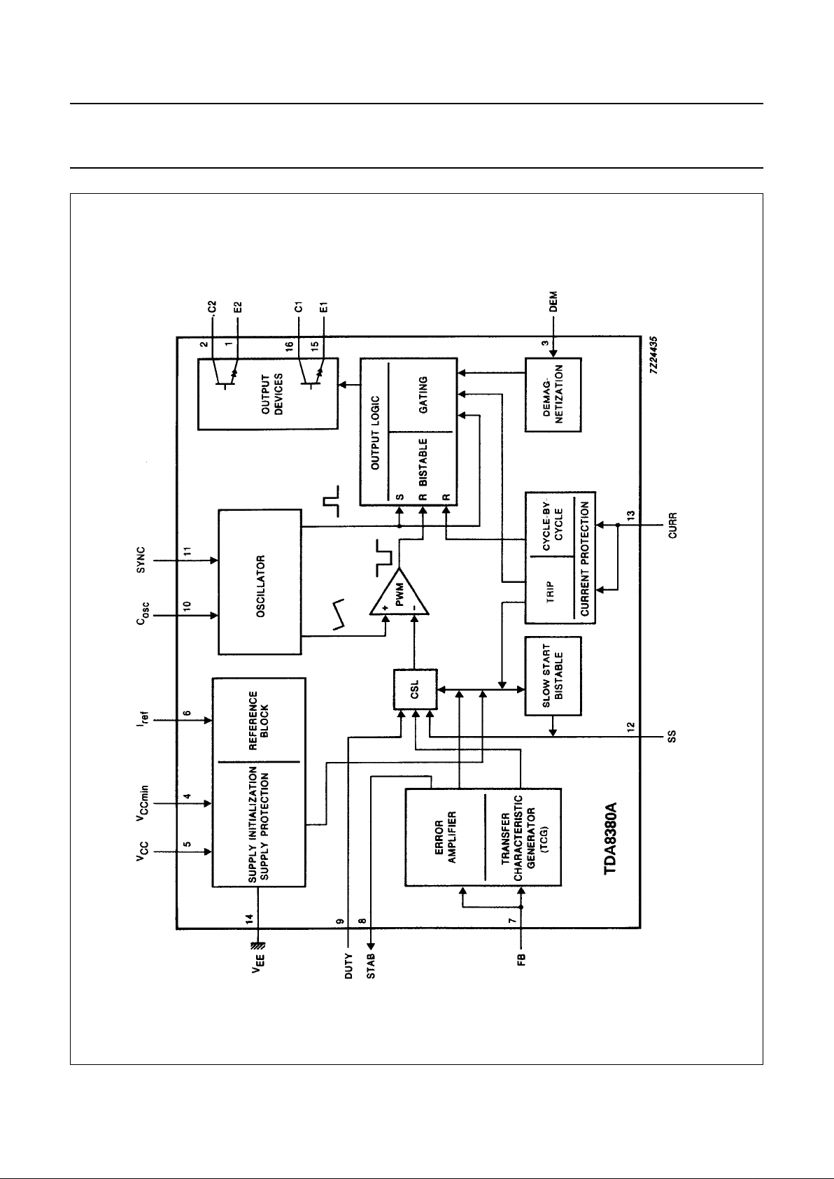
Fig.1 Block diagram.

November 1993 4
Philips Semiconductors Product specification
Control circuit for switched mode power supplies TDA8380A
PINNING
1 E2 Emitter of output source transistor
2 C2 Collector of output source transistor
3 DEM Demagnetization sense input
4V
CCmin
Minimum VCC threshold setting
5V
CC
Supply voltage
6I
ref
Reference current setting
7 FB Feedback input
8 STAB Output error amplifier
9 DUTY Pulse width modulator input
10 C
OSC
Oscillator capacitor
11 SYNC Synchronization input
12 SS Maximum duty factor (D
max
) setting plus slow-start
13 CURR Input current protection
14 V
EE
Ground
15 E1 Emitter of output sink transistor
16 C1 Collector of output sink transistor
Fig.2 Pinning diagram.

November 1993 5
Philips Semiconductors Product specification
Control circuit for switched mode power supplies TDA8380A
FUNCTIONAL DESCRIPTION
The TDA8380A is a control circuit which generates the pulses required to drive the switching transistor in a switched
mode power supply (SMPS).
Supply
This device is intended to be used on the primary side of the power supply and can be supplied via a take-over (auxiliary)
winding on the transformer.
The device is initialized via a high value resistor connected between the rectified mains voltage and the device’s supply
pin (pin 5), which causes the capacitor connected to this pin to charge slowly. When the voltage exceeds the initialization
level (typically 17 V) the device will start up and the duty cycle will be slowly increased by the slow-start circuit. After a
short period the take-over winding will supply the device. The value of the resistor is normally defined by the time taken
to charge the capacitor.
A one second delay between switching on and operation of the power supply is acceptable in most cases.
The operating voltage range is from 9 to 20 V. The supply pin is protected by a 23 V Zener diode. The supply protection
circuit is activated once the Zener diode is conducting. The slow-start procedure begins after initialization, until then the
output is off. The current drawn by the device during the initialization period is less than 150 µA.
When the supply voltage falls below the minimum trip level, the device switches off and the start-up procedure is
repeated. The minimum voltage supply threshold setting (V
CCmin
) can be set externally with a resistor connected between
the V
CCmin
pin (pin 4) and ground (pin 14) (see Fig.3).
V
CCmin
can be set between 8.4 V (an internally fixed overriding protection level) and 17 V by means of an external resistor
connected to pin 4.
When choosing the initialization and minimum supply voltages the following should be taken into account:
• The difference between the two voltages should be large enough to enable a supply voltage dip during start-up.
• The value of the minimum supply voltage should be high enough to ensure that the high-voltage transistor is correctly
driven. A high protection level makes it possible to have a large resistor value in series with the base drive.
For battery line input operation, the V
CCmin
pin is connected to VCC, the start-up circuit is then inhibited and the device
starts operating when VCC exceeds the 8.4 V protection level (this level has a hysteresis of approximately 50 mV). The
device draws current continuously under these conditions.
Fig.3 Trip level setting of minimum VCC protection level.

November 1993 6
Philips Semiconductors Product specification
Control circuit for switched mode power supplies TDA8380A
Reference block
A bandgap based reference generates a stabilized voltage of 7 V to supply most of the device’s internal circuits, this
decreases chip size and increases reliability. The only circuits connected to VCC are:
• The initialization circuit
• The output circuitry
• The series transistor of the stabilized voltage
By means of a resistor (R6) connected to the I
ref
input a reference current is defined which determines six other device
settings.
Part of the reference current is used to charge the oscillator capacitor (C10), therefore, the charging time is proportional
to R6× C10. The maximum duty factor (D
max
) is set by the resistor connected to pin 12 (R12) and is defined by the ratio
R6/R12. The minimum supply voltage (pin 5) set by the resistor (R4) at input V
CCmin
is defined by: 4/6 × V6× R4/R6.
Oscillator
The oscillator capacitor is charged and discharged between the high and low voltage levels as defined by the bandgap
reference (high voltage typically 5 V and low voltage typically 1.4 V). The charge current is 1/6 of the reference current,
the discharge current having the same value as the reference current. The period is therefore defined by 10 × R
6
× C10.
The oscillator flyback pulse is used to set the bistable in the output logic, however the output remains low until the positive
ramp starts (see Fig.4). The oscillator can be synchronized by means of the SYNC pin. When this pin is connected to
VCC, the oscillator is free running. When it is between 0.85 and 5.6 V, the oscillator stops at the low voltage level prior to
the next positive ramp.
Fig.4 Oscillator levels.
 Loading...