

INTEGRATED CIRCUITS
DATA SH EET
TDA8041H
Quadrature demodulator controller
Preliminary specification
File under Integrated Circuits, IC03
Philips Semiconductors
November 1994

Philips Semiconductors Preliminary specification
Quadrature demodulator controller TDA8041H
FEATURES
• Generates all control signals for Quadrature Phase-Shift
Keying (QPSK) and Binary Phase-Shift Keying (BPSK)
APPLICATIONS
• Demodulation of BPSK and QPSK modulated signals in
satellite and telephone applications.
demodulation
• Can be used in applications with low Eb/No and high
symbol rate (up to 30 × 106 symbols/s)
• Digital I and Q outputs (3 bits) for soft decision within
error correction
• Two matched analog-to-digital converters to quantize
the I and Q signals
• A digital detector for each control loop to generate the
required control signals
• Digital-to-analog converters and operational amplifiers
to allow high flexibility for loop time constants
• Special input stage to interface with the voltage
controlled crystal oscillator
• Positive 5 V supply voltage.
QUICK REFERENCE DATA
SYMBOL PARAMETER CONDITIONS MIN. TYP. MAX. UNIT
V
DD(A)
supply voltage for operational
4.75 5.0 5.25 V
amplifiers (pin 5)
V
DDA(C)
analog supply voltage for
4.75 5.0 5.25 V
converters (pin 20)
V
DD(I/O)
supply voltage for digital
4.75 5.0 5.25 V
inputs/outputs (pin 30)
V
DDD
supply voltage for digital
4.75 5.0 5.25 V
section (pin 35)
V
DD(C)
supply voltage for digital part
4.75 5.0 5.25 V
of ADC and DAC (pin 42)
I
DD(tot)
V
IQ
R
sym
I
O(DAC)
total supply current VDD=5 V − 30 − mA
I and Q input voltage − 1.0 − V
symbol rate −−30 × 106symbols/s
DAC output current −100 − +100 mA
ORDERING INFORMATION
TYPE NUMBER
TDA8041H QFP44
Note
1. When using reflow soldering it is recommended that the Drypack instructions in the
(order number 9398 510 63011) are followed.
November 1994 2
PACKAGE
NAME DESCRIPTION VERSION
plastic quad flat package; 44 leads (lead length 1.3 mm);
(1)
body 10 × 10 × 1.75 mm; high stand-off height
SOT307-2
“Quality Reference Handbook”
Philips Semiconductors Preliminary specification
Quadrature demodulator controller TDA8041H
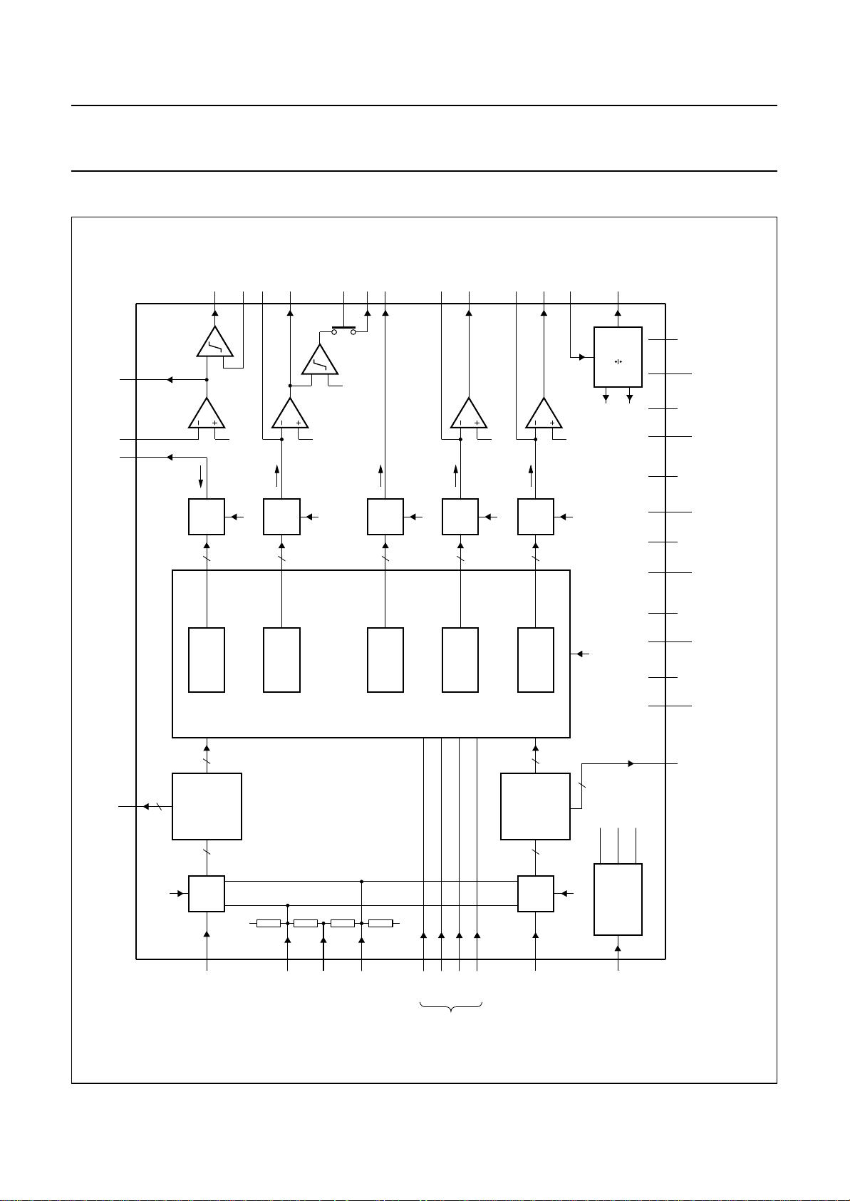
BLOCK DIAGRAM
2
LCKO
44 1
LCKDAC LCKTC
handbook, full pagewidth
IDO0 to IDO2
31 to 33
ref(mid)
CLK1
3
ADC
CLKSR
25
2
CLK2
DAC
CLK1
OPAMP
MBE167
43
V
42
35
V
34
30
V
29
24
V
20
17
V
11
6
V
26 to 28 5
QDO0 to QDO2
SS(C)
DD(C)
V
DDD
SSD
V
DD(I/O)
SS(I/O)
V
SS1
DDA(C)
V
SSA(C)
SS2
V
SS(A)
DD(A)
V
Fig.1 Block diagram.
CLKIX
CLKRO
ref(mid)
V
CLK1
CLKRTC
21
CLK
I
5
CLK
data
CLOCK
4
22
23
V
DAC
CLK1
RECOVERY
Q (3..0)
LOGIC
AGCO
CLK1
AGCTC
12
AGC
I
13
DAC
2
AGC
data
AGC
AFC2O
SWPO
ref(mid)
V
CLK1
SWEEP
39
14
th
V
LOGIC
10
AFC2
I
5
AFC2
data
DAC
AFC2
CARO
CARTC
LCKTH
LCKIO
3
4
LCK
I
DAC
4
LCK
data
LOCK
I (3..0)
4
3
LOGIC
15
ref(mid)
V
CLK1
DETECTOR
16
CAR
I
DAC
4
CAR
data
CARRIER
RECOVERY
TDA8041H
4
A
4
A
I
bias
biasIbias
I
CLK2
November 1994 3
18
ADC
ana
I
V
DD
R4
7
ref(pos)
V
R3
8
ref(mid)
V
R2
9
ref(neg)
V
R1
SS
V
383637
BQN
AFC1
mode
40
AFC2
TEST
control
19
ADC
ana
Q
CLK2
BIAS
GENERATOR
41
bias
I
Philips Semiconductors Preliminary specification
Quadrature demodulator controller TDA8041H
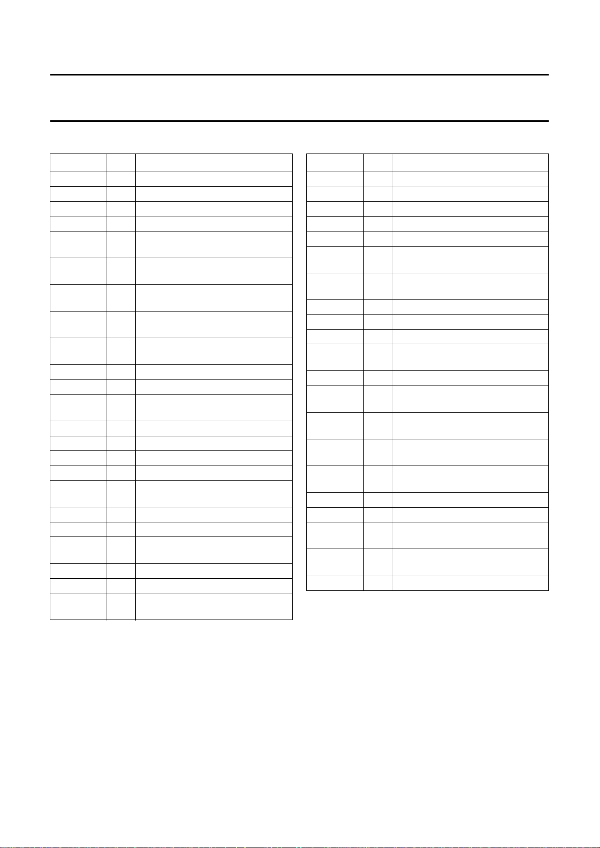
PINNING
SYMBOL PIN DESCRIPTION
LCKTC 1 carrier lock time constant
LCKO 2 carrier lock output
LCKTH 3 carrier lock threshold voltage
LCKIO 4 carrier lock indicator output
V
DD(A)
5 supply voltage for operational
amplifiers
V
SS(A)
6 negative supply voltage for
operational amplifiers
V
ref(pos)
7 positive reference voltage for
converters
V
ref(mid)
8 middle reference voltage for
converters
V
ref(neg)
9 negative reference voltage for
converters
AFC2O 10 AFC 2 output
V
SS2
11 negative supply voltage 2
AGCTC 12 automatic gain control time
constant
AGCO 13 automatic gain control output
SWPO 14 sweep current output
CARTC 15 carrier recovery time constant
CARO 16 carrier recovery output
V
SSA(C)
17 analog negative supply voltage for
converters
I
ana
Q
ana
V
DDA(C)
18 analog input I
19 analog input Q
20 analog supply voltage for
converters
CLKRTC 21 clock recovery time constant
CLKRO 22 clock recovery output
CLKIX 23 clock input from crystal circuit
(at double symbol rate)
SYMBOL PIN DESCRIPTION
V
SS1
24 negative supply voltage 1
CLKSR 25 clock output at symbol rate
QDO2 26 Q digital output (bit 2)
QDO1 27 Q digital output (bit 1)
QDO0 28 Q digital output (bit 0)
V
SS(I/O)
29 negative supply voltage for digital
inputs/outputs
V
DD(I/O)
30 supply voltage for digital
inputs/outputs
IDO2 31 I digital output (bit 2)
IDO1 32 I digital output (bit 1)
IDO0 33 I digital output (bit 0)
V
SSD
34 negative supply voltage for digital
section
V
DDD
35 supply voltage for digital section
AFC1 36 AFC control switch 1 (1 = on;
0=off)
AFC2 37 AFC control switch 2 (1 = on;
0=off)
BQN 38 BPSK/QPSK control switch
(1 = BPSK; 0 = QPSK)
SWEEP 39 sweep control switch (1 = on;
0=off)
TEST 40 test control switch (1 = on; 0 = off)
I
bias
V
DD(C)
41 input bias current for analog blocks
42 supply voltage for digital part of
ADC and DAC
V
SS(C)
43 negative supply voltage for digital
part of ADC and DAC
LCKDAC 44 carrier lock DAC output
November 1994 4
 Loading...