

INTEGRATED CIRCUITS
DATA SH EET
TDA8020HL
Dual IC card interface
Product specification
Supersedes data of 2001 Aug 15
2003 Nov 06
Philips Semiconductors Product specification
Dual IC card interface TDA8020HL
FEATURES
• Two independent 6 contacts smart card interfaces
• Supply voltage to the cards: VCC= 5 V and ICC up to
60 mA or 3 V ±5% and ICC up to 55 mA
• Integrated DC-to-DC converter (doubler, tripler or
follower) for allowing power supply from 2.7 to 6.5 V
• Independent supply voltage for interface signals (from
1.5 to 6.5 V)
• Control and status via the I2C-bus
• Four possible devices in parallel due to two I2C-bus
address pins
• Electrical specifications according to ISO 7816 or
EMV2000
• Automatic activation and deactivation sequences by
means of integrated sequencers
• Automaticclockcountandresettogglingduringwarmor
cold reset
• Interrupt request output to the controller
• 6 kV ESD protection on cards contacts
• Automatic emergency deactivation in the event of
supply drop-out, overload, overheating, card take-off or
DC-to-DC malfunctioning
• Current limitation on pins CLK, RST, I/O and V
• Integrated voltage supervisor for power-on reset and
drop-out detection.
CC
APPLICATIONS
• Set top boxes
• Banking terminals
• Internet terminals.
GENERAL DESCRIPTION
The TDA8020HL is a one-chip dual smart card interface.
Controlled by the I2C-bus, it guarantees conformity to
ISO 7816 or EMV2000 with very few external components.
ORDERING INFORMATION
TYPE NUMBER
NAME DESCRIPTION VERSION
TDA8020HL/C1 LQFP32 plastic low profile quad flat package; 32 leads; body 7 × 7 × 1.4 mm SOT358-1
TDA8020HL/C2 LQFP32 plastic low profile quad flat package; 32 leads; body 7 × 7 × 1.4 mm SOT358-1
2003 Nov 06 2
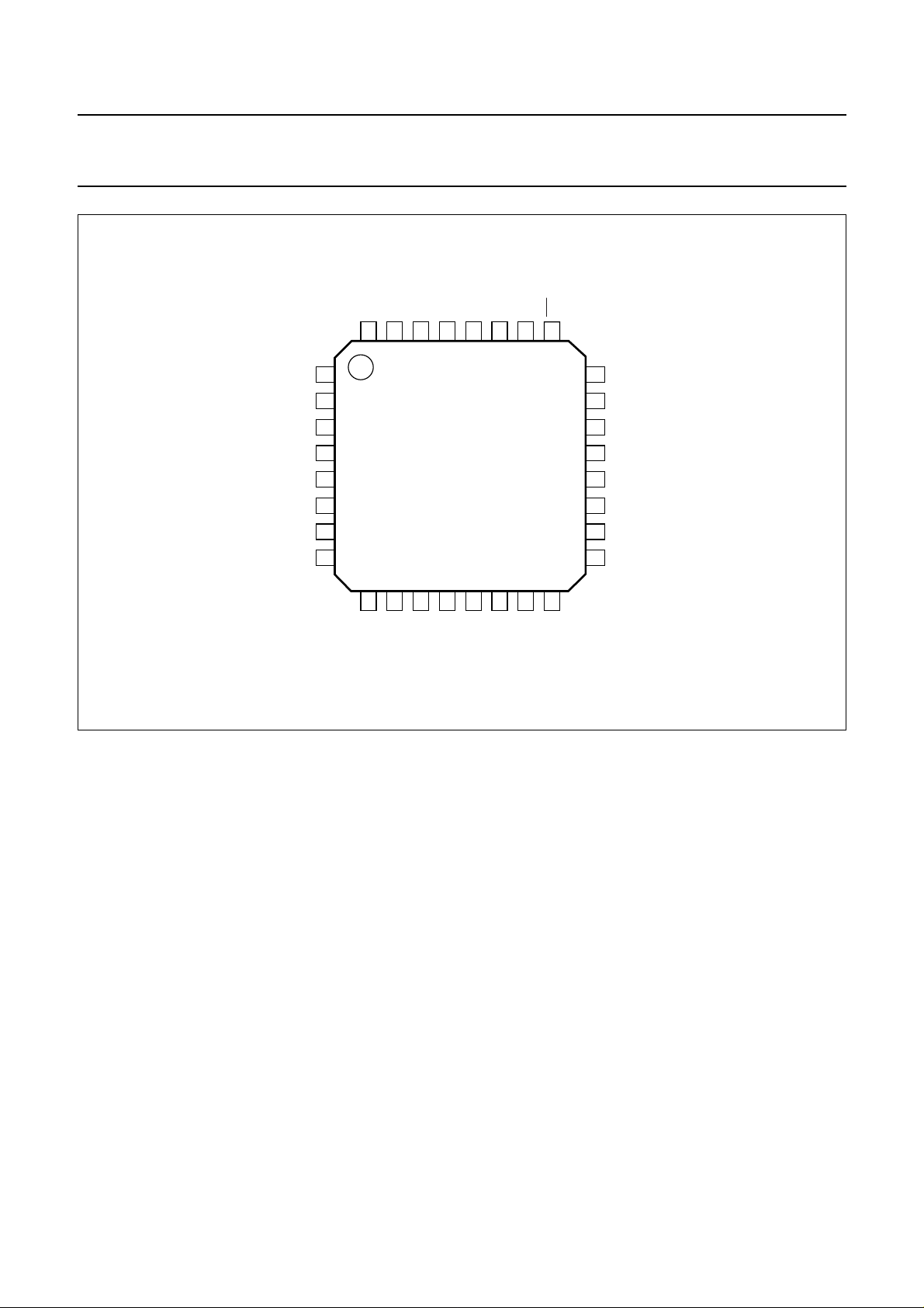
PACKAGE
Philips Semiconductors Product specification
Dual IC card interface TDA8020HL
QUICK REFERENCE DATA
SYMBOL PARAMETER CONDITIONS MIN. TYP. MAX. UNIT
Supplies
V
DD
V
DDI
I
DD
I
DDA
Card supply
, V
V
CC1
CC2
V
ripple(p-p)
I
, I
CC1
CC2
General
V
th1
V
hys1
t
de
P
tot
T
amb
supply voltage on pins VDD and
V
DDA
supply voltage for interface signals 1.5 − V
supply current VDD= 3.3 V; inactive mode −−150 µA
V
= 3.3 V; Power-down mode;
DD
2 cards activated; V
I
CC1=ICC2
= 100 µA;
CC1=VCC2
=5V;
CLK1 and CLK2 stopped
= 3.3 V; active mode;
V
DD
V
CC1=VCC2
I
CC1+ICC2
=5V;
= 80 mA;
CLK1 = CLK2 = 5 MHz
V
= 3.3 V; active mode;
DD
V
CC1=VCC2
I
CC1=ICC2
=3V;
= 10 mA;
CLK1 = CLK2 = 5 MHz
DC-to-DC converter supply current inactive mode; V
f
=10MHz
xtal
active mode; V
f
= 10 MHz; no load
xtal
DDA
DDA
=5V;
=5V;
card supply voltage including ripple 5 V card; DC ICC< 60 mA 4.75 − 5.25 V
5 V card; AC current spikes of 40 nAs 4.65 − 5.25 V
3 V card; DC I
< 55 mA 2.85 − 3.15 V
CC
3 V card; AC current spikes of 40 nAs 2.76 − 3.20 V
ripple voltage (peak-to-peak value) 20 kHz to 200 MHz −−350 mV
card supply current 0 V to 5 V −−60 mA
0Vto 3V −−55 mA
threshold voltage for the supervisor
on V
DD
hysteresis on V
th1
deactivation cycle duration 50 80 100 µs
continuous total power dissipation T
= −40 to +85 °C −−0.50 W
amb
ambient temperature TDA8020HL/C1 −30 − +85 °C
TDA8020HL/C2 −40 − +85 °C
2.7 − 6.5 V
V
DD
−−2mA
−−400 mA
−−80 mA
−−0.1 mA
−−10 mA
2.1 − 2.4 V
50 − 100 mV
2003 Nov 06 3
Philips Semiconductors Product specification
Dual IC card interface TDA8020HL
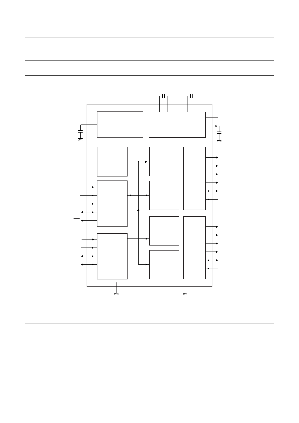
BLOCK DIAGRAM
V
I2C-BUS
AND
LEVEL
DD
SAP
20 14 19 15 17
SAM SBP SBM
DC-to-DC
CONVERTER
TDA8020HL
CLOCK
CIRCUITRY
CARD1
DRIVERS
SEQUENCER1
CLOCK
CIRCUITRY
CARD2
DRIVERS
SEQUENCER2
16
V
DDA
13
V
UP
3
CLK1
5
RST1
4
V
CC1
2
CGND1
32
I/O1
1
PRES1
9
CLK2
11
RST2
10
V
CC2
8
CGND2
6
I/O2
7
PRES2
handbook, full pagewidth
C
DEL
SAD0
SAD1
SCL
SDA
IRQ
CLKIN2
CLKIN1
I/O1uC
I/O2uC
V
DDI
SUPPLY SUPERVISOR
30
VOLTAGE REFERENCE
INTERNAL
OSCILLATOR
23
24
21
REGISTERS
22
25
29
26
27
SHIFTERS
28
31
AGND GND
Fig.1 Block diagram.
2003 Nov 06 4
1218
FCE834

Philips Semiconductors Product specification
Dual IC card interface TDA8020HL
PINNING
SYMBOL PIN TYPE DESCRIPTION
PRES1 1 I card 1 presence contact input (active HIGH)
CGND1 2 supply ground connection output to card 1 (C5 contact)
CLK1 3 O clock output to card 1 (C3 contact)
V
CC1
RST1 5 O reset output to card 1 (C2 contact)
I/O2 6 I/O I/O contact to card 2 (C7 contact); internal 15 kΩ pull-up resistance to
PRES2 7 I card 2 presence contact input (active HIGH)
CGND2 8 supply ground connection output to card 2 (C5 contact)
CLK2 9 O clock output to card 2 (C3 contact)
V
CC2
RST2 11 O reset output to card 2 (C2 contact)
GND 12 supply ground connection
V
UP
SAP 14 I/O capacitor connection for the DC-to-DC converter; a 220 nF capacitor with
SBP 15 I/O capacitor connection for the DC-to-DC converter; a 220 nF capacitor with
V
DDA
SBM 17 I/O capacitor connection for the DC-to-DC converter; a 220 nF capacitor with
AGND 18 supply analog ground for the DC-to-DC converter
SAM 19 I/O capacitor connection for the DC-to-DC converter; a 220 nF capacitor with
V
DD
SCL 21 I serial clock input of I
SDA 22 I/O serial data input/output of I
SAD0 23 I I
SAD1 24 I I
IRQ 25 O interrupt request output to host (open drain; active LOW)
CLKIN1 26 I external clock input for card 1
I/O1uC 27 I/O I/O connection to host for card 1; internal 11 kΩ pull-up resistor to V
I/O2uC 28 I/O I/O connection to host for card 2; internal 11 kΩ pull-up resistor to V
CLKIN2 29 I external clock input for card 2
C
DEL
V
DDI
I/O1 32 I/O I/O contact to card 1 (C7 contact); internal 14 kΩ pull-up resistor to V
4 supply supply voltage output to card 1 (C1 contact); decouple to pin CGND1 with
2 × 100 nF capacitors with ESR < 100 mΩ
pin V
CC2
10 supply supply voltage output to card 2 (C1 contact); decouple to pin CGND2 with
2 × 100 nF capacitors with ESR < 100 mΩ
13 I/O output of DC-to-DC converter; a 220 nF capacitor with ESR < 100 mΩ must
be connected to pin AGND
ESR < 100 mΩ must be connected between pins SAP and SAM
ESR < 100 mΩ must be connected between pins SBP and SBM
16 supply analog supply voltage for the DC-to-DC converter
ESR < 100 mΩ must be connected between pins SBP and SBM
ESR < 100 mΩ must be connected between pins SAP and SAM
20 supply power supply voltage
2
C-bus (open drain)
2
C-bus (open drain)
2
C-bus address selection input 0
2
C-bus address selection input 1
DDI
DDI
30 I/O delay capacitor connection for the voltage supervisor (1 ms per 2 nF)
31 I interface signals reference supply voltage
CC1
2003 Nov 06 5
Philips Semiconductors Product specification
Dual IC card interface TDA8020HL
handbook, full pagewidth
DEL
DDI
V
I/O1
31
32
CLKIN2
C
30
29
I/O2uC
28
I/O1uC
27
CLKIN1
26
IRQ
25
PRES1
CGND1
CLK1
V
CC1
RST1
I/O2
PRES2
CGND2
1
2
3
4
TDA8020HL
5
6
7
8
9
CLK2
10
CC2
V
11
RST2
12
GND
13
14
15
UP
SAP
V
SBP
16
DDA
V
24
23
22
21
20
19
18
17
FCE833
SAD1
SAD0
SDA
SCL
V
DD
SAM
AGND
SBM
Fig.2 Pin configuration.
2003 Nov 06 6
Philips Semiconductors Product specification
Dual IC card interface TDA8020HL
FUNCTIONAL DESCRIPTION
Throughoutthisspecification,itisassumedthatthereader
is familiar with ISO 7816 terminology.
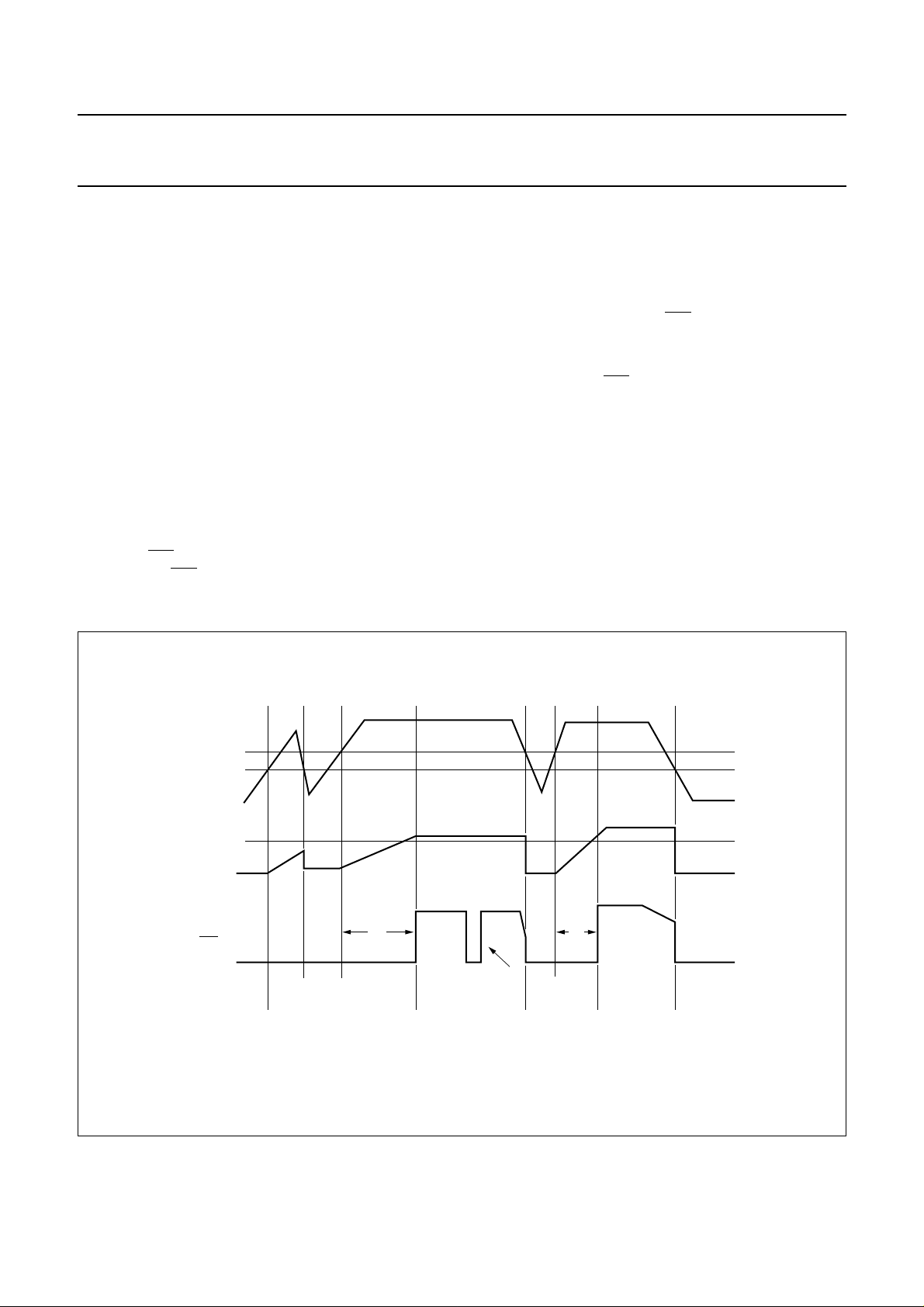
Supply
The TDA8020HL operates with a supply voltage from
2.7 to6.5 V. An integrated voltage supervisor ensures that
nospikeappearsoncardscontactsduringpower-on or off.
The supervisor also initializes the device, and forces an
automatic emergency deactivation of the contacts in the
event of a supply drop-out.
As long as the supply voltage is below the threshold
voltageV
the supply voltage reaches V
,thecapacitorC
th1
remainsuncharged.When
DEL
th1
and V
hys1
, then C
DEL
is
chargedwithasmallcurrent source of approximately 2 µA.
When the voltage on C
reaches V
DEL
, then the
th2
supervisor is no longer active. As long as the supervisor is
active (pin IRQ is LOW), bit SUPL in the status register is
set. When pin IRQ goes HIGH the voltage supervisor
becomes inactive (see Fig.3).
Separatesupplypinsareusedfor the DC-to-DC converter,
allowing specific decoupling for counteracting the noise
the switching transistors may induce on the supply.
A specific reference supply voltage, V
, is used for the
DDI
interface signals CLKIN1, CLKIN2, I/O1uC, I/O2uC,
SAD0, SAD1, SCL, SDA and IRQ, which can be lower
thanVDD(minimum 1.5 V),thusallowingdirectcontrol with
a low voltage supplied device.
Pins SCL, SDA and IRQ are open-drain outputs, and may
be externally pulled up to a voltage higher than VDD.
handbook, full pagewidth
V
V
th1
V
CDEL
DD
+ V
IRQ
hys1
V
th1
V
th2
t
w
status read
after event
BUS NOT RESPONDING BUS OK
Fig.3 Voltage supervisor.
t
w
BUS NOT
RESPONDING
BUS OK BUS NOT
RESPONDING
FCE835
2003 Nov 06 7

Philips Semiconductors Product specification
Dual IC card interface TDA8020HL
DC-to-DC converter
V
is the supply voltage for card 1 contacts and V
CC1
CC2
the supply voltage for card 2 contacts. Card 1 and card 2
may be independently powered-down, powered at 5 V or
poweredat3 V.Acapacitor type step-up converter is used
for generating these voltages. This step-up converter acts
either as a doubler, tripler or follower. An hysteresis of
100 mV is present on the different threshold voltages.
If VCCis the maximum value of V
CC1
and V
, then there
CC2
are 5 possible situations:
• VDD< 3.4 V and VCC= 3 V: in this case, the DC-to-DC
converter acts as a doubler with a regulation of
approximately 4.0 V
• VDD< 3.4 V and VCC= 5 V: in this case, the DC-to-DC
converter acts as a tripler with a regulation of
approximately 5.5 V
• VDD> 3.5 V and VCC= 3 V: in this case, the DC-to-DC
converter acts as a follower: VDD is applied on V
UP
• 5.8V>VDD> 3.5 V and VCC= 5 V: in this case, the
DC-to-DC converter acts as a doubler with a regulation
of approximately 5.5 V
• VDD> 5.9 V and VCC= 5 V: in this case, the DC-to-DC
converter acts as a follower and VDD is applied on VUP.
The output voltage, VUP, is fed internally to the V
generators. V
CC1,VCC2
and CGND1, CGND2 are used as
CC
a reference for all other cards contacts.
The sum of I
CC1
and I
shall not exceed 80 mA, which
CC2
means that when a card is drawing its maximum current
(around 60 mA at VCC= 5 V, 55 mA at VCC= 3 V), the
other card should be set in low power consumption mode
(less than 20 or 25 mA). Note that during the card Advice
to Receive (ATR) process, the current may be maximum;
so, a card should only be activated if the other card draws
lessthan20or25 mA. The DC-to-DC converter issupplied
via separate supply pins V
and AGND to allow
DDA
decoupling separate from the other supply pins.
Duringnormaloperationoractivation,each card is allowed
to draw independently a current of up to 60 mA at
VCC= 5 V or up to 55 mA at VCC= 3 V, with a supply
voltage from 2.7 V up to 6.5 V provided the sum of
I
CC1
and I
does not exceed 80 mA.
CC2
If VDD> 3 V, for 5 V cards, then both cards can draw up to
60 mA at the same time.
If VDD> 3 V, for 3 V cards, then both cards can draw up to
55 mA at the same time.
2
C-bus
I
is
A 400 kHz I2C-bus slave interface is used for configuring
the device and reading the status.
2
C-BUS PROTOCOL
I
The I2C-bus is for 2-way, 2-line communication between
different ICs or modules. The serial bus consists of two
bidirectional lines; one for data (SDA), and one for the
clock (SCL).
Both the SDA and SCL lines must be connected to a
positive supply voltage via a pull-up resistor.
The following protocol has been defined:
• Data transfer may be initiated only when the bus is not
busy
• During data transfer, the data line must remain stable
whenever the clock line is HIGH. Changes in the data
line while the clock line is HIGH will be interpreted as
control signals.
US CONDITIONS
B
The following bus conditions have been defined:
• Bus not busy: both data and clock lines remain HIGH
• Start data transfer: a change in the state of the data line,
fromHIGH-to-LOW, while the clock is HIGH, defines the
START condition
• Stop data transfer: a change in the state of the data line,
fromLOW-to-HIGH, while the clock is HIGH, defines the
STOP condition
• Data valid: the state of the data line represents valid
data when, after a START condition, the data line is
stable for the duration of the HIGH period of the clock
signal. There is one clock pulse per data bit.
DATA TRANSFER
Each data transfer is initiated with a START condition and
terminated with a STOP condition.
Data transfer is unlimited in the read mode. The
information is transmitted in bytes and each receiver
acknowledges with a ninth bit.
The TDA8020HL operates in standard mode (100 kHz
clock rate) and fast mode (400 kHz clock rate) defined in
the I2C-bus specification.
By definition, a device that sends a signal is called a
transmitter, and the device which receives the signal is
called a receiver. The device which controls the signal is
2003 Nov 06 8
Philips Semiconductors Product specification
Dual IC card interface TDA8020HL
called the master. The devices that are controlled by the
master are called slaves.
Each byte is followed by one HIGH-level acknowledge bit
asserted by the transmitter. The master generates an
extra acknowledge related clock pulse. The slave receiver
whichis addressed is obliged to generate an acknowledge
after the reception of each byte.
The master receiver must generate an acknowledge after
the reception of each byte that has been clocked out of the
slave transmitter.
The device that acknowledges has to pull-down the SDA
line during the acknowledge clock pulse in such a way that
the SDA line is stable LOW during the HIGH period of the
acknowledge related clock pulse.
Set-up and hold times must be taken into account.
A master receiver must signal an end of data to the slave
Table 1 Proposed device address bit allocations
Device
76543210
TDA8020HL 0 1 0 0 0/1 A1 A0 R/
transmitter by not generating an acknowledge on the last
byte that has been clocked out of the slave. In this event,
thetransmittermustleavethedatalineHIGHtoenablethe
master generation of the STOP condition.
See Chapter “Characteristics” for timing information.
DEVICE ADDRESSING
Each device has 2 different addresses, one for each card.
An application can use up to four devices in parallel by the
use of address selection pins SAD0 and SAD1.
Pins SAD0 and SAD1 are externally hardwired to VDD or
GND; SAD0 specifies address bit A0, SAD1 specifies
address bit A1; Address bit R/W specifies either read or
write operation: logic 1 = Read, logic 0 = Write (see
Tables 1 and 2).
Address bits
W
Table 2 Proposed I
PIN SAD1 PIN SAD0 CARD 1 CARD 2
LOW LOW 40H 48H
LOW HIGH 42H 4AH
HIGH LOW 44H 4CH
HIGH HIGH 46H 4EH
2
C-bus addresses for 4 devices in parallel
2003 Nov 06 9

Philips Semiconductors Product specification
Dual IC card interface TDA8020HL
WRITE SEQUENCE
The write sequence is as follows:
1. START condition
2. Byte 1: ADDRESS plus write command
3. ACK: acknowledge
4. Byte 2: CONTROL byte; see Table 3
5. ACK: acknowledge
6. STOP condition.
Table 3 CONTROL byte bits (all bits cleared after power-on)
BIT NAME DESCRIPTION
0START/
1 WARM when set, initiates a warm reset procedure; automatically reset by hardware when the card starts
2 3V/
3 PDOWN when set, the configuration defined by bit CLKPD is applied to pin CLK, and the circuit enters the
4 CLKPD when set, CLK is stopped HIGH during Power-down mode; when reset, CLK is stopped LOW in
5 CLKSEL1 determine the clock to the card in active mode:
6 CLKSEL2 00: CLKIN/8
7 I/OEN when set, I/O data is transferred on pin I/OuC; when reset, pin I/OuC is high-impedance
STOP when set, initiates an activation and a cold reset procedure; when reset, initiates a deactivation
sequence
answering or when the card is declared mute (once the status has been read)
5V when set; VCC= 3 V; when reset; VCC=5V
Power-down mode; when reset, the circuit goes back to normal (active) mode
Power-down mode
01: CLKIN/4
10: CLKIN/2
11: CLKIN
All frequency changes are synchronous, thus ensuring thatno pulse is shorter than 45% of the smallest period. For cards
power reduction modes, CLKIN may be stopped after switching to stop LOW or stop HIGH. CLKIN should be restarted
before leaving this mode and the selected frequency must not be changed during a CLK stop mode.
A correct duty factor can not be guaranteed in the CLKIN configuration, as it depends on the duty factor of the CLKIN
signal.
2003 Nov 06 10

Philips Semiconductors Product specification
Dual IC card interface TDA8020HL
READ STATUS SEQUENCE
The read status sequence is as follows:
1. START condition
2. Byte 1: ADDRESS plus read command
3. ACK: acknowledge
4. Byte 2: STATUS byte; see Table 4
5. ACK: acknowledge
6. STOP condition.
Table 4 STATUS byte bits (all bits cleared after power-on)
BIT NAME DESCRIPTION
0 PRES set when the card is present; reset when the card is not present
1 PRESL set when the card has been inserted or extracted; reset when the status has been read
2 I/O set when I/O is HIGH; reset when I/O is LOW
3 SUPL set when the supervisor has signalled a fault; reset when the status has been read
4 PROT set when an overload or an overheating has occurred during a session; reset when the status
has been read
5 MUTE set during ATR when the selected card has not answered during the ISO 7816 time slots; reset
when the status has been read
6 EARLY set during ATR when the selected card has answered too early; reset when the status has been
read
7 ACTIVE set if the card is active; reset if the card is inactive
When one of the bits PRESL, MUTE, EARLY and PROT is set, then IRQ goes LOW until the status byte has been read.
After power-on, bit SUPL is set until the status byte has been read, and IRQ is LOW until the supervisor becomes
inactive.
Sequencers and clock counter
Two sequencers are used to ensure activation and
deactivation sequences according to ISO 7816 and
EMV 2000, even in the event of an emergency (card
removal during transaction, supply drop-out and hardware
problem).
The sequencers are clocked by the internal oscillator.
The activation of a card is initiated by setting the card
select bit and the start bit within the control register. This is
only possible if the card is present and if the voltage
supervisor is not active.
During activation the DC-to-DC converter is initiated
(except if another card is already powered up or if
VDD= 5 V and VCC= 3 V). VCC then goes high to the
selected voltage (3 or 5 V), the I/O lines are then enabled
and the clock is started with RST LOW.
DEVICE TYPE TDA8020HL/C1:
1. If a start bit is detected on the I/O during the first
200 CLK pulses, it is ignored and the count continues.
2. If a start bit is detected between 200 and 352 CLK
pulses, bit EARLY is set in the status register.
3. Ifthe card starts responding within 41950 CLK pulses,
RST remains LOW.
4. If the card has not responded within 41950 CLK
pulses, then RST goes HIGH.
5. If a start bit is detected within 352 CLK pulses, bit
EARLY is set in the status register.
6. If the card does not respond within the next 41950
CLK pulses, bit MUTE is set within the status register.
This initiates a warm reset command.
7. If the card responds within the correct window period,
the CLK count is stopped and the system controller
may send commands to the card.
2003 Nov 06 11

Philips Semiconductors Product specification
Dual IC card interface TDA8020HL
Deactivation is initiated either by the system controller
(reset bit START), or automatically in the event of a
hardware problem or supply drop-out. With a supply
drop-out both cards are deactivated at the same time.
During deactivation, RST goes LOW, the clock is stopped
and the I/O lines go LOW. VCC then goes low with a
controlled slope and the DC-to-DC converter is stopped if
no card is active.
Outside a session, cards contacts are forced low
impedance to CGND.
DEVICE TYPE TDA8020HL/C2:
1. If a start bit is detected on the I/O during the first
200 CLK pulses, it is ignored and the count continues.
2. If a start bit is detected whilst RST is LOW (between
200 and 42100 CLK pulses), bits EARLY and MUTE
aresetinthestatusregister;RSTwill remain LOW; the
software decides whether to accept the card or not.
3. If no start bit has been detected until after 42100 CLK
pulses, RST is set to logic 1.
4. If a start bit is detected within 370 CLK pulses, bit
EARLY is set in the status register.
5. If the card does not respond within the next 42100
CLK pulses, bit MUTE is set within the status register.
This initiates a warm reset command.
6. If the card responds within the correct window period,
the CLK count is stopped and the system controller
may send commands to the card.
Activation sequence
When the cards are inactive, VCC, CLK, RST and I/O are
LOW, with low impedance with respect to CGND. The
DC-to-DC converter is stopped.
When everything is satisfactory (voltage supply, card
present and no hardware problems), the system controller
may initiate a card present activation sequence
(see Fig.4):
1. The internal oscillator changes to its high frequency
(t0).
2. TheDC-to-DCconverterisstarted(t1).Ifonecard was
already active, then the DC-to-DC converter was
already on, and nothing more occurs at this step.
3. VCC starts rising from 0 to 5 or 3 V with a controlled
rise time of 0.14 V/µs typical (t2).
4. I/O rises to VCC(t3); internal 14 kΩ pull-up resistors to
VCC.
5. CLK is sent to the card and RST is enabled (t4 = t
act
If the card does not respond within the first 42100 CLK
cycles, then RST is raised HIGH (t5).
The sequencer is clocked by f
/64 which leads to a time
int
interval T of 25 µs typical. Thus t1 = 0 to T/64;
t2 = t1 + 3T/2; t3 = t1 + 7T/2 and t4 = t1 + 4T.
).
Deactivation is initiated either by the system controller
(reset bit START), or automatically in the event of a
hardware problem or supply drop-out. With a supply
drop-out both cards are deactivated at the same time.
During deactivation, RST goes LOW, the clock is stopped
and the I/O lines go LOW. VCC then goes low with a
controlled slope and the DC-to-DC converter is stopped if
no card is active.
Outside a session, cards contacts are forced low
impedance to CGND.
2003 Nov 06 12

Philips Semiconductors Product specification
Dual IC card interface TDA8020HL
handbook, full pagewidth
START/STOP
V
UP
V
CC
I/O
CLK
RST
t0 t1 t2 t3 t4 t5
ATR
FCE837
Fig.4 Activation sequence.
Deactivation sequence
When the session is completed, the microcontroller resets bit START/STOP to logic 0 (t10). The circuit then executes an
automatic deactivation sequence (see Fig.5):
1. Card reset (RST falls LOW) (t11)
2. Clock is stopped (t12)
3. I/O falls to 0 V (t13)
4. VCC falls to 0 V with a controlled slew rate (t14)
5. The DC-to-DC converter is stopped (if both cards are inactive) and CLK, RST, VCCand I/O become low impedance
to CGND (t15)
6. The internal oscillator changes to its low frequency if both cards are inactive (t15).
t11 = t10 + T/64; t12 = t11 + T/2; t13 = t11 + T; t14 = t11 + 3T/2; t15 = t11 + 7T/2.
The deactivation time tde is the time that VCC needs to drop below 0.4 V from START/STOP to logic 0 (t10).
2003 Nov 06 13

Philips Semiconductors Product specification
Dual IC card interface TDA8020HL
handbook, full pagewidth
START/STOP
RST
CLK
I/O
V
CC
V
UP
t
de
t10 t11 t12 t13 t14 t15
Fig.5 Deactivation sequence.
VCC buffers
Each card is supplied by a separate V
buffer. Both
CC
buffers are supplied by the same multimode capacitive
DC-to-DC converter.
In all modes (follower, doubler and tripler), the DC-to-DC
converter is able to deliver 80 mA over the whole V
DD
range (2.7 to 6.5 V) or 120 mA if VDD>3V.
The current in each VCC buffer is limited internally to
around 90 mA. When one of the buffers reaches this limit,
an automatic deactivation sequence is performed.
Each VCCsupply voltage should be decoupled by an ESR
capacitor with a value of between 100 and 200 nF. If the
card socket is not very close to the device, one capacitor
should be connected close to the device, and a second
one connected close to card contact C1.
Protections
The current on pin CLK is limited to within the range
+70 mA and −70 mA.
FCE836
RST LOW, then an emergency deactivation sequence is
performed,
IRQ is pulled LOW and bit PROT is set in the
status register.
The current on pins I/O is limited to within the range
+15 mA and −15 mA.
The current on VCCis limited to 90 mA; if ICCreaches this
value, then an emergency deactivation sequence is
performed, IRQ is pulled LOW and bit PROT is set in the
status register.
In the event of overcurrent on VCC, card take-off during a
session, overheating, or overcurrent on RST, then the
TDA8020HL performs an automatic emergency
deactivation sequence on the corresponding card, resets
bit START/STOP and pulls pin IRQ LOW.
In the event of overheating or supply drop-out, or
DC-to-DC converter out of specification, the TDA8020HL
performs an automatic emergency deactivation sequence
on both cards, resets both bits START/STOP and pulls
pin IRQ LOW.
The current on pin RST is limited to within the range
+20 mA and −20 mA; if the current reaches this value with
2003 Nov 06 14

Philips Semiconductors Product specification
Dual IC card interface TDA8020HL
Clock inputs and data inputs/outputs to the system controller
CLKIN1 is the input clock for card 1, CLKIN2 for card 2. They may be driven separately from the system controller, or be
tied together externally and driven by the same signal.
I/O1uC is the data signal to or from card 1, I/O2uC to or from card 2. They can be driven separately from the system
controller, in which case both bits I/OEN may be set to logic 1. They can also be driven by the same signal, which
requires them to be tied together externally, but each bit I/OEN has to be set or reset according to the addressed card.
LIMITING VALUES
In accordance with the Absolute Maximum Rating System (IEC 60134).
SYMBOL PARAMETER CONDITION MIN. MAX. UNIT
V
DD
V
DDI
V
n
P
tot
T
stg
T
j
V
esd
supply voltage on pins VDD and V
DDA
−0.5 +6.5 V
supply voltage for interface signals −0.5 +6.5 V
input voltage
on pins SAP, SAM, SBP, SBM and V
UP
−0.5 +7.5 V
on pins SDA and SCL −0.5 +6.5 V
on all other pins −0.5 VDD+ 0.5 V
total power dissipation T
= −40 °C to +85 °C − 500 mW
amb
storage temperature −55 +150 °C
junction temperature − 125 °C
electrostatic discharge voltage HMB; note 1
all card contact pins
−6+6kV
within the typical
application; note 2
pins V
DDA
and V
DDI
−0.5 +0.5 kV
all other pins −2+2kV
MM; note 3
all pins −200 +200 V
Notes
1. HBM: EIA/JESD22-A 114-B; June 2000.
2. All card contacts are protected against any short-circuit with any other card contact.
3. MM: EIA/JESD22-A 115-A; October 1997.
HANDLING
Inputs and outputs are protected against electrostatic discharge in normal handling. However it is good practice to take
normal precautions appropriate to handling MOS devices (see
“Handling MOS devices”
).
THERMAL CHARACTERISTICS
SYMBOL PARAMETER CONDITIONS VALUE UNIT
R
th(j-a)
thermal resistance from junction to ambient in free air 80 K/W
2003 Nov 06 15

Philips Semiconductors Product specification
Dual IC card interface TDA8020HL
CHARACTERISTICS
VDD= 3.3 V; V
SYMBOL PARAMETER CONDITIONS MIN. TYP. MAX. UNIT
Temperature
T
amb
Supply
V
DD
I
DD
V
DDI
I
DDI
V
th1
V
hys1
V
th2
V
CDEL
I
CDEL
t
W
DC-to-DC converter
f
int
V
UP
V
dt
= 1.5 V; f
DDI
CLKIN1=fCLKIN2
= 10 MHz; GND = 0 V; T
amb
=25°C.
ambient temperature TDA8020HL/C1 −30 − +85 °C
TDA8020HL/C2 −40 − +85 °C
supply voltage on pins V
and V
DDA
supply current (IDDand I
DD
) inactive mode −−150 µA
DDA
Power-down mode; 2 cards
activated; V
I
CC1=ICC2
CC1=VCC2
= 100 µA; CLK1 and
=5V;
2.7 − 6.5 V
−−2.5 mA
CLK2 stopped
active mode; V
I
CC1+ICC2
=80mA;
CC1=VCC2
=5V;
−−300 mA
CLK1 = CLK2 = 5 MHz
active mode; V
I
CC1=ICC2
=10mA;
CC1=VCC2
=3V;
−−80 mA
CLK1 = CLK2 = 5 MHz
supply voltage for interface
1.5 − V
DD
V
signals
supply current for interface
−−120 µA
signals
threshold voltage for
supervisor on V
hysteresis on V
DD
th1
threshold voltage on
pin C
DEL
voltage on pin C
output current at pin C
DEL
DEL
width of the internal ALARM
falling 2.1 − 2.4 V
50 − 100 mV
− 1.38 − V
−−V
+ 0.3 V
DD
pin grounded (charge) −−2−µA
V
CDEL=VDD
C
CDEL
(discharge) − 5 − mA
=22nF − 10 − ms
pulse
internal oscillator frequency 2 2.5 3.2 MHz
voltage on pin V
UP
at least one 5 V card − 5.5 − V
both 3 V cards − 4 − V
detectionvoltagefordoubler,
− 3.4 − V
tripler and follower selection
2003 Nov 06 16

Philips Semiconductors Product specification
Dual IC card interface TDA8020HL
SYMBOL PARAMETER CONDITIONS MIN. TYP. MAX. UNIT
Card supply voltages (pins V
V
CC(inactive)
output voltage in inactive
mode
I
CC(inactive)
output current from V
CC1
and V
CC
); note 1
CC2
no load 0 − 0.1 V
I
= 1 mA 0 − 0.3 V
inactive
pin grounded −−−1mA
when inactive
V
CC(active)
output voltage in active
mode including ripple
ICC< 60 mA; 5 V card;
I
CC1+ICC2
<80mA;
2.7V<VDD< 6.5 V
< 55 mA; 3 V card;
I
CC
I
CC1+ICC2
<80mA;
2.7V<VDD< 6.5 V
current pulses of 40 nAs with
I < 200 mA and t < 400 ns;
f < 20 MHz; 5 V card
current pulses of 24 nAs with
I < 200 mA and t < 400 ns;
f < 20 MHz; 3 V card
V
CC(load)
output voltage when both
card interfaces fully loaded
active mode; VDD>3V;
I
< 60 mA; I
CC1
CC2
< 60 mA;
5 V cards
active mode; V
ICC< 55 mA; I
DD
CC2
>3V;
<55mA;
3 V cards
I
CC(max)
maximum output current from 0 to 5 V (5 V card); the other
card at full load; VDD>3V
from 0 to 3 V (3 V card); the other
DD
>3V
I
CC(sc)
V
ripple(p-p)
card at full load; V
short-circuit current VCC shorted to GND −−−100 mA
ripple voltage (peak-to-peak
from 20 kHz to 200 MHz −−350 mV
value)
SR slew rate up or down for 5 V card (maximum
capacitance is 300 nF)
up or down for 3 V card (maximum
capacitance is 300 nF)
Reset output to the cards (pins RST1 and RST2)
V
o(inactive)
I
o(inactive)
output voltage in inactive
mode
output current from pin RST
no load 0 − 0.1 V
= 1 mA 0 − 0.3 V
I
inactive
pin grounded 0 −−1mA
when inactive
V
OL
V
OH
t
r
t
f
LOW-level output voltage IOL= 200 µA0−0.3 V
HIGH-level output voltage IOH< −200 µAV
rise time CL=30pF −−0.1 µs
fall time CL=30pF −−0.1 µs
4.75 5 5.25 V
2.8 3 3.2 V
4.6 − 5.4 V
2.76 − 3.24 V
4.6 − 5.4 V
2.76 − 3.24 V
−−−60 mA
−−−55 mA
0.08 0.14 0.20 V/µs
0.05 0.09 0.13 V/µs
− 0.5 − V
CC
CC
V
2003 Nov 06 17

Philips Semiconductors Product specification
Dual IC card interface TDA8020HL
SYMBOL PARAMETER CONDITIONS MIN. TYP. MAX. UNIT
Clock output to the cards (pins CLK1 and CLK2)
V
o(inactive)
output voltage in inactive
mode
I
o(inactive)
output current from pin CLK
when inactive
V
OL
V
OH
t
r
t
f
f
clk
LOW-level output voltage IOL= 200 µA0−0.3 V
HIGH-level output voltage IOH< −200 µAV
rise time CL=30pF −−8ns
fall time CL=30pF −−8ns
clock frequency operational 0 − 10 MHz
δ duty factor C
SR slew rate (rise and fall) C
Data lines (pins I/O1 and I/O2); note 2
V
o(inactive)
output voltage in inactive
mode
I
o(inactive)
current from pin I/O when
inactive
V
OL
V
OH
I
edge
LOW-level output voltage IOL= 1 mA 0 − 0.3 V
HIGH-level output voltage no DC load 0.9V
current from pins I/O1
and I/O2 when active pull-up
t
d(edge)
delay between falling edge
on pins I/O1, I/O2 and width
of active pull-up pulse
V
IL
V
IH
I
IL
LOW-level input voltage −0.3 − +0.8 V
HIGH-level input voltage 1.5 − V
LOW-level input current on
pin I/O
I
LIH
HIGH-level input leakage
current on pin I/O
t
i(r),ti(f)
t
o(r),to(f)
C
i
input transition times from V
output transition times CL< 30 pF; no DC load;
input capacitance on
pins I/O1 and I/O2
R
f
max
pu(int)
internal pull-up resistance
between pin I/O and V
CC
maximum frequency on
pins I/O1 and I/O2
no load 0 − 0.1 V
I
= 1 mA 0 − 0.3 V
inactive
pin grounded 0 −−1mA
− 0.5 − V
CC
=30pF 45 − 55 %
L
= 30 pF 0.2 −− V/ns
L
CC
V
no load 0 − 0.1 V
I
=1mA −−0.3 V
inactive
pin grounded −−−1mA
− VCC+ 0.1 V
CC
I
< −20 µA 0.8V
OH
< −40 µA 0.75V
I
OH
− VCC+ 0.1 V
CC
− VCC+ 0.1 V
CC
VOH= 0.9 VCC; CL=30pF −1 −− mA
− 500 650 ns
CC
V
VIL= 0; VCC=5V −−600 µA
V
= 0; VCC=3V −−500 µA
IL
VIH=V
CC
IL(max)
to V
IH(min)
−−10 µA
−−1.5 µs
−−0.1 µs
10% to 90% from 0 V to
V
and V
CC1
CC2
−−10 pF
10 14 18 kΩ
−−500 kHz
2003 Nov 06 18

Philips Semiconductors Product specification
Dual IC card interface TDA8020HL
SYMBOL PARAMETER CONDITIONS MIN. TYP. MAX. UNIT
Data lines (pins I/O1uC and I/O2uC); note 3
V
OL
V
OH
V
IL
V
IH
I
IL
I
LIH
t
, t
i(r)
i(f)
t
, t
o(r)
o(f)
R
pu(int)
Timing
t
act
t
de
Protections and limitations
I
CC(sd)
I
I/O(lim)
I
CLK(lim)
I
RST(sd)
T
j(sd)
Card presence inputs (pins PRES1 and PRES2)
V
IL
V
IH
I
LIL
I
LIH
LOW-level output voltage IOL= 1 mA 0 − 0.4 V
HIGH-level output voltage no DC load 0.9V
I
< −10 µA 0.75V
OH
LOW-level input voltage −0.3 − +0.25V
HIGH-level input voltage 0.7V
DDI
DDI
DDI
− V
− V
− V
DDI
DDI
DDI
+ 0.2 V
+ 0.2 V
DDI
+ 0.3 V
V
LOW-level input current VIL=0 −−600 µA
HIGH-level input leakage
VIH=V
DDI
−−10 µA
current
input transition times from V
output transition times CL< 30 pF; 10% to 90% from
0VtoV
internal pull-up resistance between I/O1uC, I/O2uC and V
IL(max)
DDI
to V
IH(min)
−−1 µs
−−0.1 µs
71115kΩ
DDI
activation sequence duration −−135 µs
deactivation sequence
−−110 µs
duration
shutdown and limitation
current at V
CC1
and V
limitation current on
CC2
normal mode −−90 − mA
Power-down mode −−12 − mA
−15 − +15 mA
pins I/O1 and I/O2
limitation current on
−70 − +70 mA
pins CLK1 and CLK2
shutdown and limitation
−20 − +20 mA
current on pins RST1
and RST2
shutdown die temperature − 150 −°C
LOW-level input voltage −−0.3V
HIGH-level input voltage 0.7V
LOW-level input leakage
VI=0V −−±20 µA
−− V
DD
DD
V
current
HIGH-level input leakage
VI=V
DD
−−±20 µA
current
2003 Nov 06 19

Philips Semiconductors Product specification
Dual IC card interface TDA8020HL
SYMBOL PARAMETER CONDITIONS MIN. TYP. MAX. UNIT
Clock inputs (pins CLKIN1 and CLKIN2)
f
ext
external frequency applied
on CLKIN1 and CLKIN2
V
IL
V
IH
t
, t
i(r)
i(f)
LOW-level input voltage V
HIGH-level input voltage V
>2V 0 − 0.3V
DDI
1.5V<V
> 2 V 0.7V
DDI
1.5V<V
<2V 0 − 0.15V
DDI
< 2 V 0.85V
DDI
input transition times −−0.1/f
Logic inputs (pins SAD0 and SAD1)
V
IL
V
IH
I
LIL
LOW-level input voltage −0.3 − +0.3V
HIGH-level input voltage 0.7V
LOW-level input leakage
current
I
LIH
HIGH-level input leakage
current
C
i
input capacitance −−10 pF
Interrupt line (pin IRQ ; open-drain; active LOW output)
V
OL
I
LH
LOW-level output voltage Io=2mA −−0.3 V
HIGH-level leakage current −−10 µA
Serial data input/output (pin SDA; open-drain)
V
IL
V
IH
I
LH
I
IL
V
OL
LOW-level input voltage −0.3 − 0.3V
HIGH-level input voltage 0.7V
HIGH-level leakage current −−1 µA
LOW-level input current depends on the pull-up resistance −−−
LOW-level output voltage IOL=3mA −−0.3 V
Serial clock input (pin SCL; open-drain)
V
IL
V
IH
I
LH
I
IL
2
C-bus timings; see Figures 6 and 7
I
f
SCL
t
BUF
LOW-level input voltage −0.3 − 0.3V
HIGH-level input voltage 0.7V
HIGH-level leakage current −−1 µA
LOW-level input current depends on the pull-up resistance −−−
clock frequency 0 − 400 kHz
bus free time between a
STOP and START condition
t
HD;STA
START condition hold time
after which first clock pulse
is generated
t
LOW
t
HIGH
t
SU;STA
SCL LOW time 1.3 −− µs
SCL HIGH time 0.6 −− µs
set-up time START condition repeated start 0.6 −− µs
0 − 25 MHz
DDI
+ 0.3 V
+ 0.3 V
DDI
+ 0.3 V
V
V
ns
V
DDI
DDI
DDI
− V
− V
− V
DDI
DDI
DDI
CLKIN
DDI
−−±20 µA
−−±20 µA
V
V
− 6.5 V
DD
− 6.5 V
DD
DD
DD
1.3 −− µs
0.6 −− µs
2003 Nov 06 20

Philips Semiconductors Product specification
Dual IC card interface TDA8020HL
SYMBOL PARAMETER CONDITIONS MIN. TYP. MAX. UNIT
t
HD;DAT
t
SU;DAT
t
r
t
f
t
SU;STO
Notes
1. Two ceramic multilayer capacitors of minimum 100 nF with low ESR should be used in order to meet these
specifications.
2. Pin I/O1 has an internal 14 kΩ pull-up resistor to V
3. Pins I/O1uC and I/O2uC have an internal 11 kΩ pull-up resistor to V
4. The hold time required (not greater than 300 ns) to bridge the undefined region of the falling edge of SCL must be
internally provided by a transmitter.
data hold time note 4 0 −− ns
data set-up time 100 −− ns
rise time SDA and SCL −−300 ns
fall time SDA and SCL −−300 ns
set-up time STOP condition 0.6 −− µs
and pin I/O2 has an internal 14 kΩ pull-up resistor to V
CC1
.
DDI
CC2
.
handbook, full pagewidth
handbook, full pagewidth
SDA
SCL
SDA
SCL
S
START condition
t
BUF
Fig.6 START and STOP conditions.
t
LOW
t
HD;STA
t
r
t
HD;DAT
P
STOP condition
t
f
t
HIGH
MBC622
t
SU;DAT
SDA
SCL
SDA
MGA728
Fig.7 I2C-bus timing waveforms.
2003 Nov 06 21
t
SU;STA
t
SU;STO

This text is here in white to force landscape pages to be rotated correctly when browsing through the pdf in the Acrobat reader.This text is here in
_white to force landscape pages to be rotated correctly when browsing through the pdf in the Acrobat reader.This text is here inThis text is here in
white to force landscape pages to be rotated correctly when browsing through the pdf in the Acrobat reader. white to force landscape pages to be ...
2003 Nov 06 22
handbook, full pagewidth
APPLICATION INFORMATION
Philips Semiconductors Product specification
Dual IC card interface TDA8020HL
CARD_READ_LM01
CARD 1
CARD_READ_LM01
CARD 2
0 kΩ
C4
C8
C3
C7
C2
C6
C1
C5
C5I
C1I
C6I
C2I
C7I
C3I
C8I
C4I
K1
K2
0 kΩ
100 kΩ
C4
C8
C3
C7
C2
C6
C1
C5
C5I
C1I
C6I
C2I
C7I
C3I
C8I
C4I
K1
K2
100
nF
100 nF
100
nF
3.3 V
3.3 V
100 kΩ
100 kΩ
PRES1
CGND1
CLK1
V
CC1
RST1
I/O2
PRES2
CGND2
100 nF
1.5 V
10 µF
(16 V)
100 nF
I/O1
32 31 30 29 28 27 26 25
1
2
3
4
5
6
7
8
9 10111213141516
CLK2
V
V
DDI
CC2
22 nF
DEL
CLKIN2
C
TDA8020HL
GND
RST2
I/O2uC
UP
V
I/O1uC
SAP
220 nF
220 Ω
IRQ
CLKIN1
24
23
22
21
20
19
18
17
SBP
220
DDA
V
100 nF
33 µF
(16 V)
3.3 V 3.3 V
SAD1
SAD0
SDA
SCL
V
DD
SAM
AGND
SBM
nF
10 pF
220 nF
100 nF
10 µF
(16 V)
3.3 V to 6.5 V
1 kΩ
1.5 V
1.5 to
6.5 kΩ
10 µF
P1_0
P1_1
P1_2
P1_3
P1_4
P1_5
P1_6
P1_7
RST
P3_0
P3_1
P3_2
P3_3
P3_4
P3_5
P3_6
P3_7
XTAL2
XTAL1
V
1
2
3
4
5
6
7
8
9
10
11
12
13
14
15
16
17
18
19
SS
20
33 pF
14.745 MHz
33 pF
1.5 V
V
CC
40
P0_0
39
P0_1
38
P0_2
37
P0_3
36
P0_4
35
P0_5
34
P0_6
33
P0_7
32
EA
31
ALE
30
PSEN
29
P2_7
28
P2_6
MICROCONTROLLER
27
P2_5
26
P2_4
25
P2_3
24
P2_2
23
P2_1
22
P2_0
21
FCE838
Fig.8 Application diagram.

Philips Semiconductors Product specification
Dual IC card interface TDA8020HL
PACKAGE OUTLINE
LQFP32: plastic low profile quad flat package; 32 leads; body 7 x 7 x 1.4 mm
c
y
X
24 17
25
pin 1 index
32
1
16
Z
E
e
w M
b
p
9
8
A
H
E
E
A
2
A
SOT358-1
(A )
A
1
L
detail X
3
θ
L
p
e
w M
b
p
D
H
D
Z
D
B
v M
0 2.5 5 mm
scale
DIMENSIONS (mm are the original dimensions)
UNIT
mm
A
max.
1.6
A
1A2A3bp
0.20
1.45
1.35
0.25
0.05
cE
0.4
0.18
0.3
0.12
(1)
(1) (1)(1)
D
7.1
6.9
eH
7.1
6.9
0.8
9.15
8.85
Note
1. Plastic or metal protrusions of 0.25 mm maximum per side are not included.
OUTLINE
VERSION
IEC JEDEC JEITA
REFERENCES
SOT358 -1 136E03 MS-026
2003 Nov 06 23
v M
H
D
A
B
9.15
8.85
LL
E
0.75
0.45
p
0.25 0.11 0.2
EUROPEAN
PROJECTION
Z
D
0.9
0.5
Zywv θ
E
o
0.9
7
o
0.5
0
ISSUE DATE
00-01-19
03-02-25

Philips Semiconductors Product specification
Dual IC card interface TDA8020HL
SOLDERING
Introduction to soldering surface mount packages
Thistextgivesaverybriefinsighttoacomplex technology.
A more in-depth account of soldering ICs can be found in
our
“Data Handbook IC26; Integrated Circuit Packages”
(document order number 9398 652 90011).
There is no soldering method that is ideal for all surface
mount IC packages. Wave soldering can still be used for
certainsurfacemountICs,butitisnot suitable for fine pitch
SMDs. In these situations reflow soldering is
recommended.
Reflow soldering
Reflow soldering requires solder paste (a suspension of
fine solder particles, flux and binding agent) to be applied
totheprinted-circuitboardbyscreenprinting,stencillingor
pressure-syringe dispensing before package placement.
Driven by legislation and environmental forces the
worldwide use of lead-free solder pastes is increasing.
Several methods exist for reflowing; for example,
convection or convection/infrared heating in a conveyor
type oven. Throughput times (preheating, soldering and
cooling) vary between 100 and 200 seconds depending
on heating method.
Typical reflow peak temperatures range from
215 to 270 °C depending on solder paste material. The
top-surface temperature of the packages should
preferably be kept:
• below 225 °C (SnPb process) or below 245 °C (Pb-free
process)
– for all BGA, HTSSON-T and SSOP-T packages
– for packages with a thickness ≥ 2.5 mm
– for packages with a thickness < 2.5 mm and a
volume ≥ 350 mm3 so called thick/large packages.
• below 240 °C (SnPb process) or below 260 °C (Pb-free
process) for packages with a thickness < 2.5 mm and a
volume < 350 mm3 so called small/thin packages.
Moisture sensitivity precautions, as indicated on packing,
must be respected at all times.
If wave soldering is used the following conditions must be
observed for optimal results:
• Use a double-wave soldering method comprising a
turbulent wave with high upward pressure followed by a
smooth laminar wave.
• For packages with leads on two sides and a pitch (e):
– larger than or equal to 1.27 mm, the footprint
longitudinal axis is preferred to be parallel to the
transport direction of the printed-circuit board;
– smaller than 1.27 mm, the footprint longitudinal axis
must be parallel to the transport direction of the
printed-circuit board.
The footprint must incorporate solder thieves at the
downstream end.
• Forpackageswithleadsonfoursides,the footprint must
be placed at a 45° angle to the transport direction of the
printed-circuit board. The footprint must incorporate
solder thieves downstream and at the side corners.
During placement and before soldering, the package must
be fixed with a droplet of adhesive. The adhesive can be
applied by screen printing, pin transfer or syringe
dispensing. The package can be soldered after the
adhesive is cured.
Typical dwell time of the leads in the wave ranges from
3 to 4 seconds at 250 °C or 265 °C, depending on solder
material applied, SnPb or Pb-free respectively.
A mildly-activated flux will eliminate the need for removal
of corrosive residues in most applications.
Manual soldering
Fix the component by first soldering two
diagonally-opposite end leads. Use a low voltage (24 V or
less) soldering iron applied to the flat part of the lead.
Contact time must be limited to 10 seconds at up to
300 °C.
When using a dedicated tool, all other leads can be
soldered in one operation within 2 to 5 seconds between
270 and 320 °C.
Wave soldering
Conventional single wave soldering is not recommended
forsurfacemountdevices(SMDs)orprinted-circuitboards
with a high component density, as solder bridging and
non-wetting can present major problems.
To overcome these problems the double-wave soldering
method was specifically developed.
2003 Nov 06 24

Philips Semiconductors Product specification
Dual IC card interface TDA8020HL
Suitability of surface mount IC packages for wave and reflow soldering methods
SOLDERING METHOD
WAVE REFLOW
(2)
BGA, HTSSON-T
PACKAGE
(3)
, LBGA, LFBGA, SQFP, SSOP-T
(1)
(3)
, TFBGA,
not suitable suitable
USON, VFBGA
DHVQFN, HBCC, HBGA, HLQFP, HSO, HSOP, HSQFP, HSSON,
not suitable
(4)
suitable
HTQFP, HTSSOP, HVQFN, HVSON, SMS
(5)
PLCC
LQFP, QFP, TQFP not recommended
SSOP, TSSOP, VSO, VSSOP not recommended
PMFP
, SO, SOJ suitable suitable
(5)(6)
suitable
(7)
suitable
(8)
not suitable not suitable
Notes
1. FormoredetailedinformationontheBGApackagesrefertothe
“(LF)BGAApplicationNote
”(AN01026);orderacopy
from your Philips Semiconductors sales office.
2. All surface mount (SMD) packages are moisture sensitive. Depending upon the moisture content, the maximum
temperature (with respect to time) and body size of the package, there is a risk that internal or external package
cracks may occur due to vaporization of the moisture in them (the so called popcorn effect). For details, refer to the
Drypack information in the
“Data Handbook IC26; Integrated Circuit Packages; Section: Packing Methods”
.
3. These transparent plastic packages are extremely sensitive to reflow soldering conditions and must on no account
be processed through more than one soldering cycle or subjected to infrared reflow soldering with peak temperature
exceeding 217 °C ± 10 °C measured in the atmosphere of the reflow oven. The package body peak temperature
must be kept as low as possible.
4. These packages are not suitable for wave soldering. On versions with the heatsink on the bottom side, the solder
cannot penetrate between the printed-circuit board and the heatsink. On versions with the heatsink on the top side,
the solder might be deposited on the heatsink surface.
5. If wave soldering is considered, then the package must be placed at a 45° angle to the solder wave direction.
The package footprint must incorporate solder thieves downstream and at the side corners.
6. Wave soldering is suitable for LQFP, TQFP and QFP packages with a pitch (e) larger than 0.8 mm; it is definitely not
suitable for packages with a pitch (e) equal to or smaller than 0.65 mm.
7. Wave soldering is suitable for SSOP, TSSOP, VSO and VSSOP packages with a pitch (e) equal to or larger than
0.65 mm; it is definitely not suitable for packages with a pitch (e) equal to or smaller than 0.5 mm.
8. Hot bar or manual soldering is suitable for PMFP packages.
2003 Nov 06 25
Philips Semiconductors Product specification
Dual IC card interface TDA8020HL
DATA SHEET STATUS
LEVEL
DATA SHEET
STATUS
(1)
PRODUCT
STATUS
(2)(3)
DEFINITION
I Objective data Development This data sheet contains data from the objective specification for product
development. Philips Semiconductors reserves the right to change the
specification in any manner without notice.
II Preliminary data Qualification This data sheet contains data from the preliminary specification.
Supplementary data will be published at a later date. Philips
Semiconductors reserves the right to change the specification without
notice, in order to improve the design and supply the best possible
product.
III Product data Production This data sheet contains data from the product specification. Philips
Semiconductors reserves the right to make changes at any time in order
to improve the design, manufacturing and supply. Relevant changes will
be communicated via a Customer Product/Process Change Notification
(CPCN).
Notes
1. Please consult the most recently issued data sheet before initiating or completing a design.
2. The product status of the device(s) described in this data sheet may have changed since this data sheet was
published. The latest information is available on the Internet at URL http://www.semiconductors.philips.com.
3. For data sheets describing multiple type numbers, the highest-level product status determines the data sheet status.
DEFINITIONS
DISCLAIMERS
Short-form specification The data in a short-form
specification is extracted from a full data sheet with the
same type number and title. For detailed information see
the relevant data sheet or data handbook.
Limiting values definition Limiting values given are in
accordance with the Absolute Maximum Rating System
(IEC 60134). Stress above one or more of the limiting
values may cause permanent damage to the device.
These are stress ratings only and operation of the device
attheseoratanyotherconditionsabovethosegiveninthe
Characteristics sections of the specification is not implied.
Exposure to limiting values for extended periods may
affect device reliability.
Application information Applications that are
described herein for any of these products are for
illustrative purposes only. Philips Semiconductors make
norepresentationorwarrantythatsuch applications will be
suitable for the specified use without further testing or
modification.
Life support applications These products are not
designed for use in life support appliances, devices, or
systems where malfunction of these products can
reasonably be expected to result in personal injury. Philips
Semiconductorscustomersusingorsellingthese products
for use in such applications do so at their own risk and
agree to fully indemnify Philips Semiconductors for any
damages resulting from such application.
Right to make changes Philips Semiconductors
reserves the right to make changes in the products including circuits, standard cells, and/or software described or contained herein in order to improve design
and/or performance. When the product is in full production
(status ‘Production’), relevant changes will be
communicated via a Customer Product/Process Change
Notification (CPCN). Philips Semiconductors assumes no
responsibility or liability for the use of any of these
products, conveys no licence or title under any patent,
copyright, or mask work right to these products, and
makes no representations or warranties that these
products are free from patent, copyright, or mask work
right infringement, unless otherwise specified.
2003 Nov 06 26

Philips Semiconductors Product specification
Dual IC card interface TDA8020HL
PURCHASE OF PHILIPS I2C COMPONENTS
Purchase of Philips I
components in the I2C system provided the system conforms to the I2C specification defined by
Philips. This specification can be ordered using the code 9398 393 40011.
2
C components conveys a license under the Philips’ I2C patent to use the
2003 Nov 06 27

Philips Semiconductors – a w orldwide compan y
Contact information
For additional information please visit http://www.semiconductors.philips.com. Fax: +31 40 27 24825
For sales offices addresses send e-mail to: sales.addresses@www.semiconductors.philips.com.
© Koninklijke Philips Electronics N.V. 2003
All rights are reserved. Reproduction in whole or in part is prohibited without the prior written consent of the copyright owner.
The information presented in this document does not form part of any quotation or contract, is believed to be accurate and reliable andmaybechanged
without notice. No liability will be accepted by the publisher for any consequence of its use. Publication thereof does not convey nor imply any license
under patent- or other industrial or intellectual property rights.
Printed in The Netherlands 753504/03/pp28 Date of release: 2003 Nov 06 Document order number: 9397750 11554
SCA75
 Loading...