Philips TDA8020HL Datasheet
INTEGRATED CIRCUITS
DATA SH EET
TDA8020HL
Dual smart card interface
Product specification
Supersedes data of 2001 May 29
File under Integrated Circuits, IC02
2001 Aug 15

Philips Semiconductors Product specification
Dual smart card interface TDA8020HL
FEATURES
• Two independent 6 contacts smart card interfaces
• Supply voltage tothe cards; VCC=5or3V±5%; ICCup
to 65 mA
• Integrated DC/DC converter(doubler, tripler or follower)
for allowing power supply from 2.5 to 6.5 V
• Independant supply voltage for interface signals (from
1.5 to 6.5 V)
• Control and status via the I2C-bus
• Four possible devices in parallel due to two I2C-bus
address pins
• Electrical specifications according to ISO 7816 or
EMV norms
• Automatic activation and deactivation sequences by
means of integrated sequencers
• Automaticclock count and resettoggling during warm or
cold reset
• Interrupt request output to the controller
• 6 kV ESD protection on cards contacts
• Automatic emergency deactivation in the event of
supply drop-out, overload, overheating or card take-off
• Current limitation on pins CLK, RST, I/O and V
• Integrated voltage supervisor for power-on reset and
drop-out detection
• Power-down mode with several wake-up events.
CC
APPLICATIONS
• Set top boxes
• Banking terminals
• Internet terminals.
GENERAL DESCRIPTION
The TDA8020HL is a one-chip dual smart card interface.
Controlled by the I2C-bus, it guarantees conformity to
ISO 7816 or EMV norms with very few external
components.
ORDERING INFORMATION
TYPE
NUMBER
TDA8020HL LQFP32 plastic low profile quad flat package; 32 leads; body 7 × 7 × 1.4 mm SOT358-1
2001 Aug 15 2
NAME DESCRIPTION VERSION
PACKAGE
Philips Semiconductors Product specification
Dual smart card interface TDA8020HL
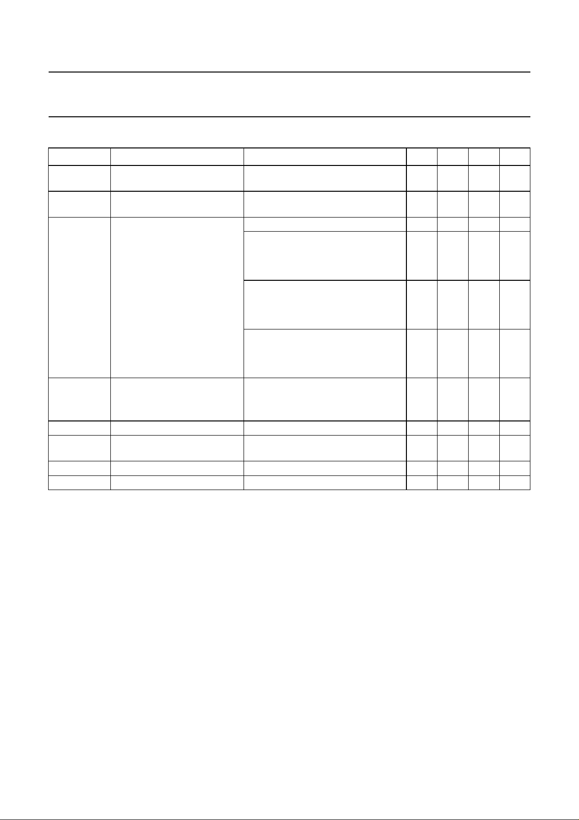
QUICK REFERENCE DATA
SYMBOL PARAMETER CONDITIONS MIN. TYP. MAX. UNIT
V
V
I
DD
V
I
CC1
V
V
T
DD
DDI
CC1
th1
hys1
amb
, V
CC2
, I
CC2
supplyvoltageonpins VDDand
V
DDA
supply voltage for interface
2.5 − 6.5 V
1.5 − V
DD
V
signals
supply current (IDDand I
)VDD= 3.3 V; inactive mode −−150 µA
DDA
V
= 3.3 V; Power-down mode;
DD
2 cards activated; V
I
CC1=ICC2
= 100 µA;
CC1=VCC2
=5V;
−−2mA
CLK1 and CLK2 stopped
= 3.3 V; active mode;
V
DD
V
CC1=VCC2
I
CC1+ICC2
=5V;
=80mA;
−−400 mA
CLK1 = CLK2 = 5 MHz
V
= 3.3 V; active mode;
DD
V
CC1=VCC2
I
CC1=ICC2
=3V;
=10mA;
−−80 mA
CLK1 = CLK2 = 5 MHz
supply voltage for card 1 and 2 note 1
5 V card 4.75 − 5.25 V
3 V card 2.80 − 3.20 V
supply current for card 1 and 2 0 − 55 mA
threshold voltage for the
supervisor on V
hysteresis on V
DD
th1
2.1 − 2.4 V
50 − 100 mV
ambient temperature −25 − +85 °C
Note
1. Both cards are not allowed to operate at maximum current at the same time at minimum supply voltage.
2001 Aug 15 3
Philips Semiconductors Product specification
Dual smart card interface TDA8020HL
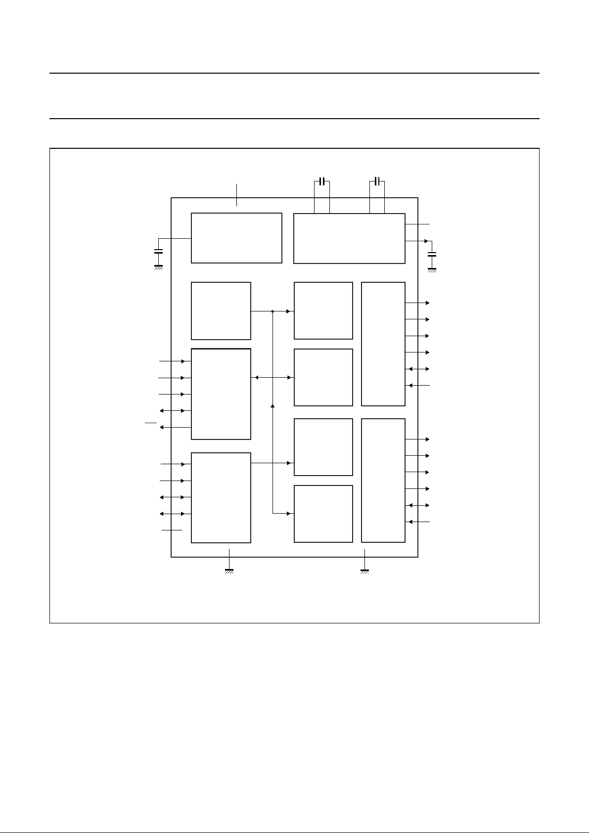
BLOCK DIAGRAM
V
I2C-BUS
AND
LEVEL
DD
SAP
20 14 19 15 17
SAM SBP SBM
DC/DC
CONVERTER
TDA8020HL
CLOCK
CIRCUITRY
CARD1
DRIVERS
SEQUENCER1
CLOCK
CIRCUITRY
CARD2
DRIVERS
SEQUENCER2
16
V
DDA
13
V
UP
3
CLK1
5
RST1
4
V
CC1
2
CGND1
32
I/O1
1
PRES1
9
CLK2
11
RST2
10
V
CC2
8
CGND2
6
I/O2
7
PRES2
handbook, full pagewidth
C
DEL
SAD0
SAD1
SCL
SDA
IRQ
CLKIN2
CLKIN1
I/O1uC
I/O2uC
V
DDI
SUPPLY SUPERVISOR
30
VOLTAGE REFERENCE
INTERNAL
OSCILLATOR
23
24
21
REGISTERS
22
25
29
26
27
SHIFTERS
28
31
AGND GND
Fig.1 Block diagram.
2001 Aug 15 4
1218
FCE834
Philips Semiconductors Product specification
Dual smart card interface TDA8020HL
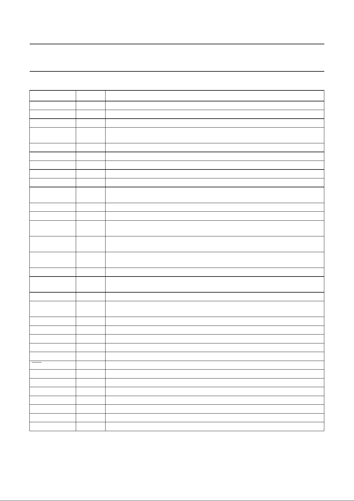
PINNING
SYMBOL PIN DESCRIPTION
PRES1 1 card 1 presence contact input (active HIGH)
CGND1 2 ground connection output to card 1 (C5 contact)
CLK1 3 clock output to card 1 (C3 contact)
V
CC1
RST1 5 reset output to card 1 (C2 contact)
I/O2 6 I/O contact to card 2 (C7 contact); internal 15 kΩ pull-up resistance to pin V
PRES2 7 card 2 presence contact input (active HIGH)
CGND2 8 ground connection output to card 2 (C5 contact)
CLK2 9 clock output to card 2 (C3 contact)
V
CC2
RST2 11 reset output to card 2 (C2 contact)
GND 12 ground connection
V
UP
SAP 14 capacitors connection for the DC/DC converter; a 220 nF capacitor with
SBP 15 capacitors connection for the DC/DC converter; a 220 nF capacitor with
V
DDA
SBM 17 capacitors connection for the DC/DC converter; a 220 nF capacitor with
AGND 18 analog ground connection for the DC/DC converter
SAM 19 capacitors connection for the DC/DC converter; a 220 nF capacitor with
V
DD
SCL 21 serial clock input of the I
SDA 22 serial data input/output of the I
SAD0 23 I
SAD1 24 I
IRQ 25 interrupt request output to host (open drain; active LOW)
CLKIN1 26 external clock input for card 1
I/O1uC 27 I/O connection to host for card 1; internal 22 kΩ pull-up resistor to V
I/O2uC 28 I/O connection to host for card 2; internal 22 kΩ pull-up resistor to V
CLKIN2 29 external clock input for card 2
C
DEL
V
DDI
I/O1 32 I/O contact to card 1 (C7 contact); internal 15 kΩ pull-up resistor to V
4 supply voltage output to card 1 (C1 contact); decouple to pin CGND1 with 2 × 100 nF
capacitors with ESR < 100 mΩ
CC2
10 supply voltage output to card 2 (C1 contact); decouple to pin CGND2 with 2 × 100 nF
capacitors with ESR < 100 mΩ
13 output of DC/DC converter; a 220 nF capacitor with ESR < 100 mΩ mustbe connected
to pin AGND
ESR < 100 mΩ must be connected between pins SAP and SAM
ESR < 100 mΩ must be connected between pins SBP and SBM
16 analog supply voltage for the DC/DC converter
ESR < 100 mΩ must be connected between pins SBP and SBM
ESR < 100 mΩ must be connected between pins SAP and SAM
20 power supply voltage
2
C-bus (open drain)
2
C-bus (open drain)
2
C-bus address selection input 0
2
C-bus address selection input 1
DDI
DDI
30 delay capacitor connection for the voltage supervisor (1 ms per 2 nF)
31 interface signals reference supply voltage
CC1
2001 Aug 15 5

Philips Semiconductors Product specification
Dual smart card interface TDA8020HL
handbook, full pagewidth
DEL
DDI
V
I/O1
31
32
CLKIN2
C
30
29
I/O2uC
28
I/O1uC
27
CLKIN1
26
IRQ
25
PRES1
CGND1
CLK1
V
CC1
RST1
I/O2
PRES2
CGND2
1
2
3
4
TDA8020HL
5
6
7
8
9
CLK2
10
CC2
V
11
RST2
12
GND
13
14
15
UP
SAP
V
SBP
16
DDA
V
24
23
22
21
20
19
18
17
FCE833
SAD1
SAD0
SDA
SCL
V
DD
SAM
AGND
SBM
Fig.2 Pin configuration.
2001 Aug 15 6
Philips Semiconductors Product specification
Dual smart card interface TDA8020HL
FUNCTIONAL DESCRIPTION
Throughoutthis specification, it isassumed that the reader
is familiar with ISO 7816 norm terminology.
Supply
The TDA8020HL operates with a supply voltage from
2.5 to6.5 V. An integratedvoltage supervisor ensures that
nospikeappears on cards contacts duringpower-onoroff.
The supervisor also initializes the device, and forces an
automatic emergency deactivation of the contacts in the
event of a supply drop-out.
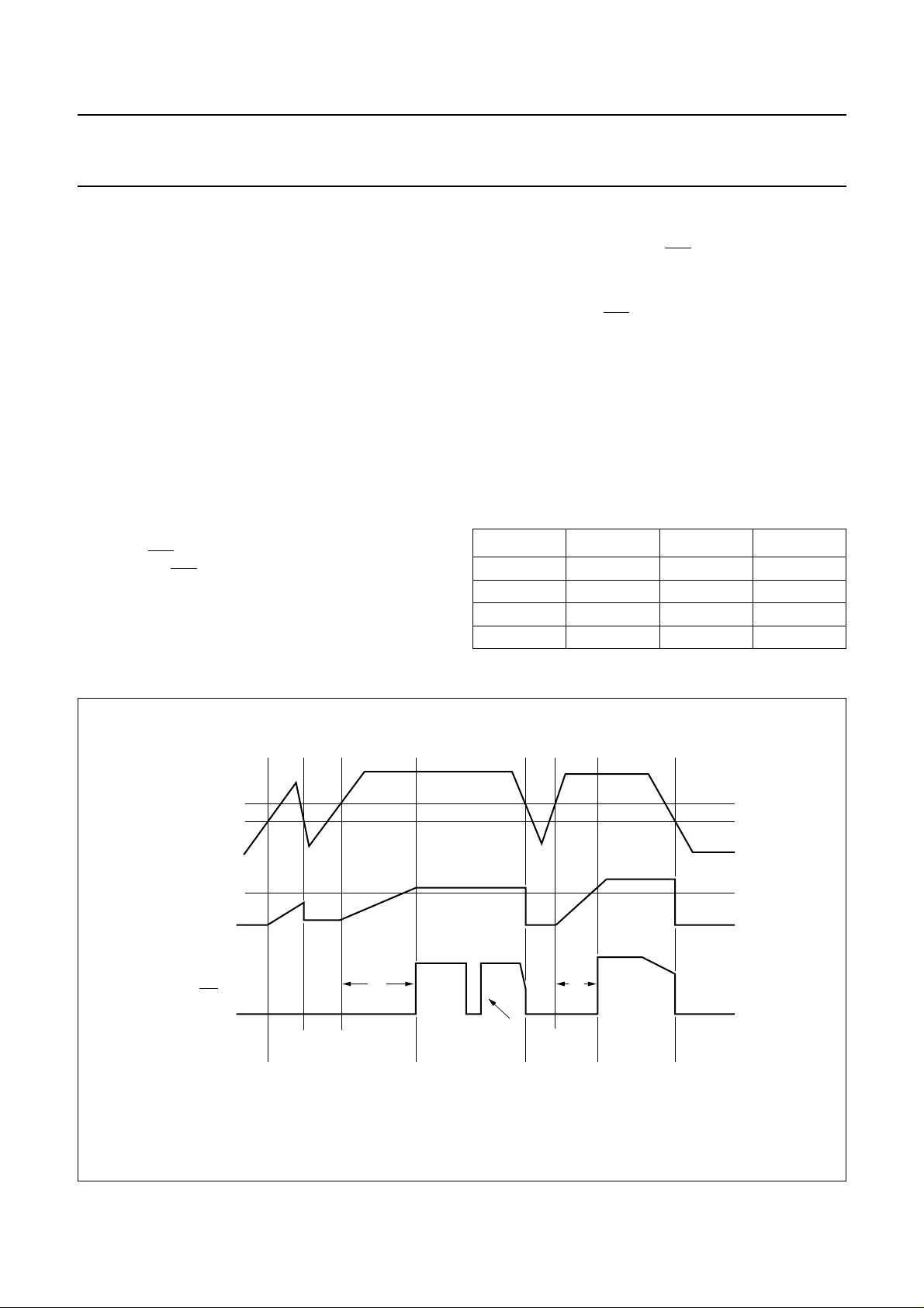
As long as the supply voltage is below the threshold
voltageV
the supply voltage reaches V
,thecapacitorC
th1
remainsuncharged.When
DEL
th1
and V
hys1
, then C
DEL
is
chargedwithasmall current source of approximately 2 µA.
When the voltage on C
reaches V
DEL
, then the
th2
supervisor is no longer active. As long asthe supervisor is
active (pin IRQ is LOW), bit SUPL in the status register is
set. When pin IRQ goes HIGH the supervisor becomes
inactive (see Fig.3).
Separate supply pins are used for the DC/DC converter,
allowing specific decoupling for counteracting the noise
the switching transistors may induce on the supply.
A specific reference supply voltage, V
, is used for the
DDI
interface signals CLKIN1, CLKIN2, I/O1uC, I/O2uC,
SAD0, SAD1, SCL, SDA and IRQ, which can be lower
thanVDD(minimum 1.5 V),thusallowingdirectcontrolwith
a low voltage supplied device.
Pins SCL, SDA and IRQ are open-drain outputs, and may
be externally pulled up to a voltage higher than VDD.
2
C-bus
I
A 400 kHz I2C-bus slave interface is used for configuring
the device and reading the status. The bus has
2 addresses, one for each card. 4 devices may be used in
paralleldue to the addressselectionpins SAD0 and SAD1
(see Table 1).
Table 1 Proposed addresses
PIN SAD1 PIN SAD0 CARD 1 CARD 2
LOW LOW 40H 48H
LOW HIGH 42H 4AH
HIGH LOW 44H 4CH
HIGH HIGH 46H 4EH
handbook, full pagewidth
V
V
th1
V
CDEL
DD
+ V
IRQ
hys1
V
th1
V
th2
t
w
BUS NOT RESPONDING BUS OK
Fig.3 Supply supervisor.
2001 Aug 15 7
status read
after event
t
w
BUS NOT
RESPONDING
BUS OK BUS NOT
RESPONDING
FCE835
Philips Semiconductors Product specification
Dual smart card interface TDA8020HL
WRITING COMMANDS
START, ADDRESS, WRITE, CONTROL byte, STOP.
Table 2 CONTROL bits (all bits cleared after power-on)
NAME BIT DESCRIPTION
START/
WARM 1 when set, initiates a warm reset procedure; automatically reset by hardware when the card
3 and
PDOWN 3 when set, the configuration defined by bit CLKPD is applied on pin CLK, and the circuit
CLKPD 4 when set, CLK is stopped HIGH during Power-downmode; when reset, CLK is stopped LOW
CLKSEL1 5 bits 5 and 6 determine the clock to the card in normal mode according to Table 3
CLKSEL2 6
I/OEN 7 when set, I/O is transferred on I/OuC; when reset, I/O to I/OuC is high-impedance
STOP 0 when set, initiates an activation and a cold reset procedure; when reset, initiates a
deactivation sequence
starts answering or when the card is declared mute
5 V 2 when set, VCC= 3 V; when reset, VCC=5V
enters the Power-down mode; when reset, the circuit goes back to normal (active) mode
in Power-down mode
When deactivating the card, by resetting the START bit,
only bit 0 must be changed.
The clock to the cards in active mode is selected with
bits CLKSEL1 and CLKSEL2; see Table 3.
Table 3 Selecting the card clock.
BIT CLKSEL2 BIT CLKSEL1
0 0 CLKIN/8
0 1 CLKIN/4
1 0 CLKIN/2
1 1 CLKIN
CLOCK
OUTPUT
All frequency changes are synchronous, thus ensuring
that no pulse is shorter than 45% of the smallest period.
For cards power reduction modes, CLKINmay be stopped
after switching to STOP LOW or STOP HIGH. CLKIN
should be restarted before leaving this mode.
A correct duty factor can not be guaranteed in the CLKIN
configuration, as it depends on the duty factor of the
CLKIN signal.
2001 Aug 15 8
 Loading...