

Philips TDA8012AM Datasheet

INTEGRATED CIRCUITS
DATA SH EET
TDA8012AM
Low power PLL FM demodulator for
satellite TV receivers
Product specification
File under Integrated Circuits, IC02
1997 May 26

Philips Semiconductors Product specification
Low power PLL FM demodulator for
TDA8012AM
satellite TV receivers
FEATURES
• High input sensitivity
• Fully balanced two-pin Voltage Controlled Oscillator
(VCO)
• Low input impedance (50 Ω)
• Low impedance video baseband output
• Internal voltage stabilizer
• Keyed Automatic Frequency Control (AFC) or peak AFC
• Carrier detector
• Automatic Gain Control (AGC) output.
APPLICATIONS
• Digital Broadcast System (DBS) satellite receivers.
QUICK REFERENCE DATA
SYMBOL PARAMETER CONDITIONS MIN. TYP. MAX. UNIT
V
CC
I
CC
V
i
f
c
V
o(p-p)
supply voltage 4.75 5.0 5.25 V
supply current VCC=5V; T
input level 53 57 61 dBµV
operating carrier frequency − 480 − MHz
video output signal amplitude
frequency deviation = 25 MHz − 1 − V
(peak-to-peak value)
GENERAL DESCRIPTION
The TDA8012AM is a sensitive Phase Locked Loop (PLL)
Frequency Modulation (FM) demodulator for the second
Intermediate Frequency (IF) in satellite receivers.
It provides Automatic Gain Control (AGC) and Automatic
Frequency Control (AFC) outputs that can be used to
optimize the level and the frequency of the signal applied
at the input. During the search procedure, the AFC output
provides a signal used for carrier detection.
=25°C 405060mA
amb
ORDERING INFORMATION
TYPE
NUMBER
NAME DESCRIPTION VERSION
PACKAGE
TDA8012AM SSOP20 plastic shrink small outline package; 20 leads; body width 4.4 mm SOT266-1
1997 May 26 2
Philips Semiconductors Product specification
Low power PLL FM demodulator for
satellite TV receivers
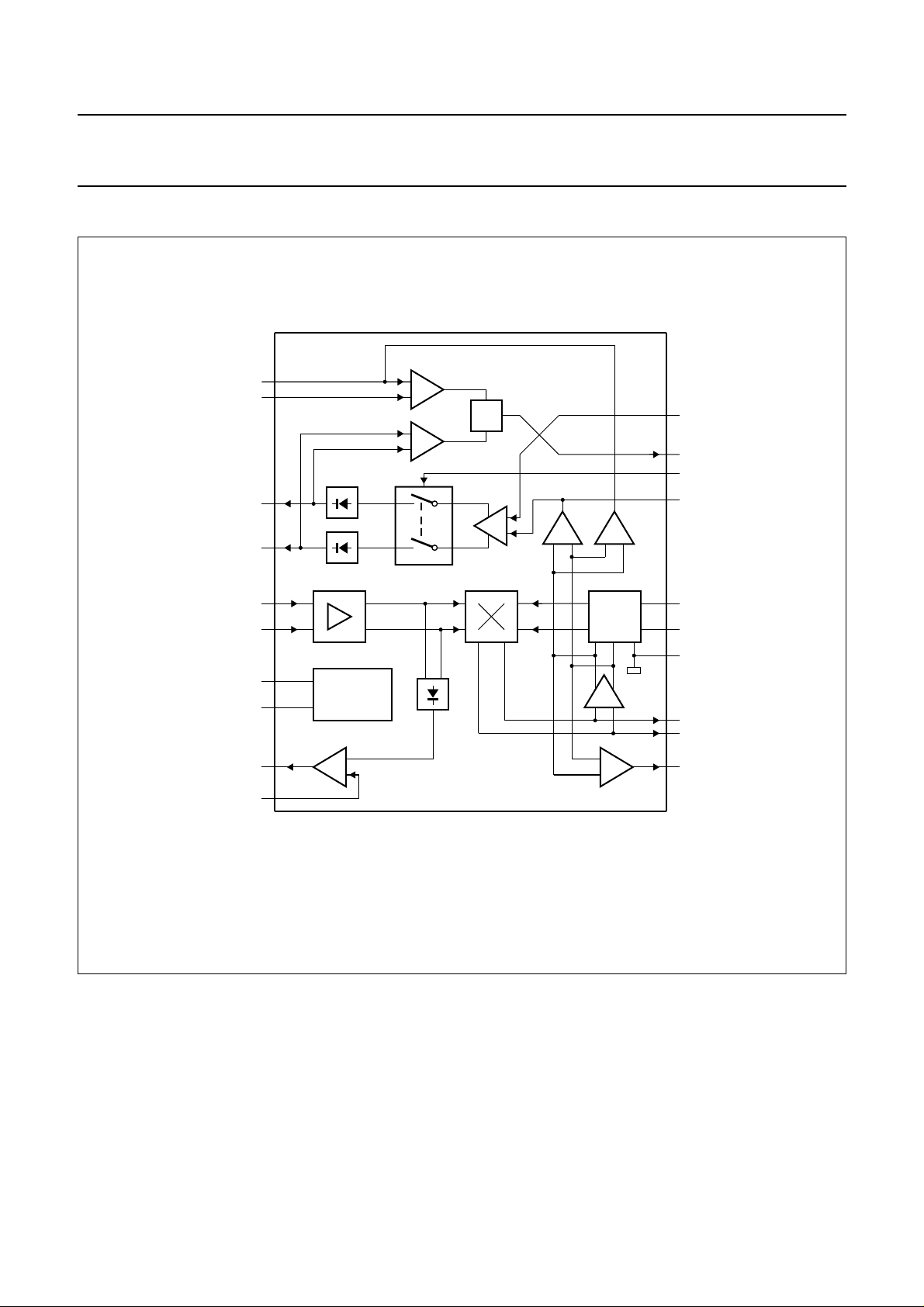
BLOCK DIAGRAM
handbook, full pagewidth
PD
PD
1
2
3
+
4
−
CDF1
CDF2
CARRIER
DETECTOR
AFC
20
19
18
17
TDA8012AM
AFCOS
AFC/CDO
KEY
AFCF
AGCO
V
th(AGC)
IFI1
IFI2
GND
V
CC
5
6
7
8
9
10
STABILIZER
AGC
TDA8012AM
Fig.1 Block diagram.
VCO
VIDEO BUFFER
16
15
14
13
12
11
VCO2
VCO1
OSCGND
LF2
LF1
VIDEO
MBH934
1997 May 26 3
Philips Semiconductors Product specification
Low power PLL FM demodulator for
satellite TV receivers
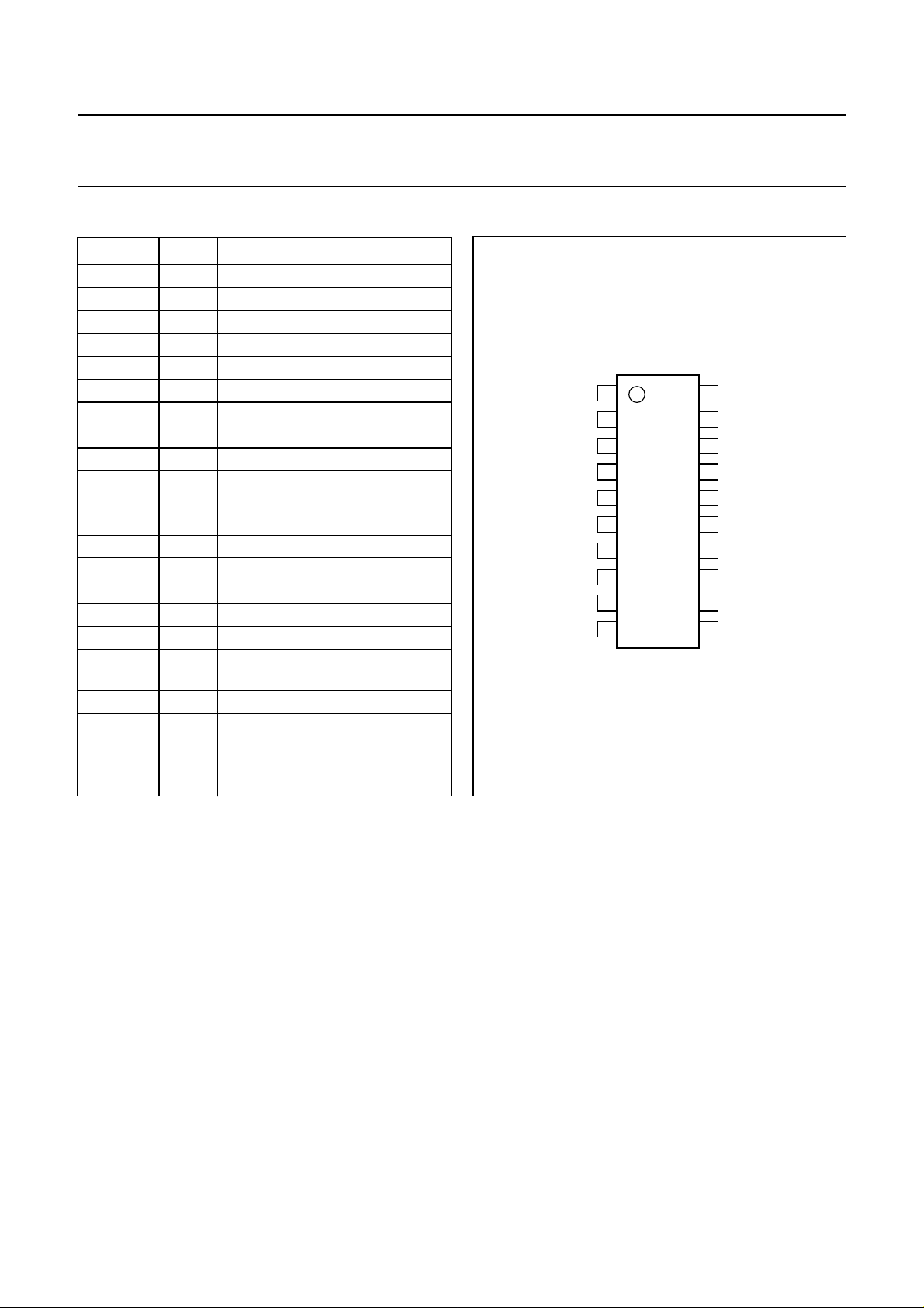
PINNING
SYMBOL PIN DESCRIPTION
CDF1 1 carrier detector filter 1 input
CDF2 2 carrier detector filter 2 input
PD+ 3 positive peak detector output
PD− 4 negative peak detector output
IFI1 5 intermediate frequency input 1
IFI2 6 intermediate frequency input 2
GND 7 general ground
V
CC
AGCO 9 automatic gain control output
V
th(AGC)
VIDEO 11 baseband signal output
LF1 12 loop filter 1 input
LF2 13 loop filter 2 input
OSCGND 14 oscillator ground
VCO1 15 oscillator tank circuit 1 input
VCO2 16 oscillator tank circuit 2 input
AFCF 17 automatic frequency control filter
KEY 18 key pulse input
AFC/CDO 19 automatic frequency control
AFCOS 20 automatic frequency control of fset
8 supply voltage
10 automatic gain control threshold
voltage input
input
/carrier detector output
input
handbook, halfpage
V
1
CDF1
2
CDF2
+
PD
3
−
4
PD
IFI1
5
TDA8012AM
6
IFI2
GND
7
V
8
CC
AGCO
9
th(AGC)
10
Fig.2 Pin configuration.
TDA8012AM
20
AFCOS
AFC/CDO
19
KEY
18
17
AFCF
VCO2
16
15
VCO1
OSCGND
14
13
LF2
LF1
12
11
VIDEO
MBH931
FUNCTIONAL DESCRIPTION
The TDA8012AM is a low power PLL FM demodulator
designed for use in satellite TV reception systems.
The demodulator is based on a PLL structure including a
fully balanced two-pin VCO. A high gain IF amplifier
ensures a high input sensitivity. The video output voltage
is supplied through a highly-linear video buffer with a low
output impedance. The centre frequency of the VCO and
the loop characteristics can be set by external components
(see Fig.4).
1997 May 26 4
The circuit provides an AGC signal which is used to drive
a gain-controlled IF amplifier (TDA8011T or TDA8010AM)
for a stable PLL demodulation characteristic.
An analog AFC voltage is available. This signal fits in with
the input of the A/D converter port of the PLL frequency
synthesizer (TSA5055). The AFC function may be keyed
to address D2MAC systems.
The TDA8012AM includes a Carrier Detector (CD) used
for channel detection during search procedures.

Philips Semiconductors Product specification
Low power PLL FM demodulator for
TDA8012AM
satellite TV receivers
LIMITING VALUES
In accordance with the Absolute Maximum Rating System (IEC 134).
SYMBOL PARAMETER MIN. MAX. UNIT
V
CC
V
I(max)
I
O(max)
t
sc(max)
Z
L
T
stg
T
j
T
amb
HANDLING
Inputs and outputs are protected against electrostatic discharge in normal handling. However, to be totally safe it is
desirable to take normal precautions appropriate to handling MOS devices.
supply voltage −0.3 +6.0 V
voltage on all pins −0.3 V
CC
V
output source current − 10 mA
maximum short-circuit time on outputs − 10 s
AC load impedance at video output 600 −Ω
IC storage temperature −55 +150 °C
junction temperature − 150 °C
operating ambient temperature −10 +80 °C
THERMAL CHARACTERISTICS
SYMBOL PARAMETER CONDITIONS VALUE UNIT
R
th j-a
thermal resistance from junction to ambient in free air 120 K/W
1997 May 26 5
 Loading...