

Philips tda8011 DATASHEETS

INTEGRATED CIRCUITS
DATA SH EET
TDA8011T
IF amplifier for satellite TV receivers
Product specification
File under Integrated Circuits, IC02
Philips Semiconductors
February 1995
Philips Semiconductors Product specification
IF amplifier for satellite TV receivers TDA8011T
FEATURES
• High voltage gain, up to 860 MHz
• Low noise
• Large dynamic gain control
• High impedance differential input stage
• Low output impedance.
DESCRIPTION
The TDA8011T is a broadband low-noise AGC amplifier
which is used for the second IF amplifier in satellite TV
receivers. The amplifier is powered from a single 5 V
supply. The amplifier gain can be easily controlled over a
large dynamic range by using a single ground reference
voltage. The two outputs are 180° out of phase and are
separately buffered. The two outputs can therefore, be
used in either the differential or asymmetrical mode.
APPLICATIONS
• Second IF amplifier for satellite TV receivers.
QUICK REFERENCE DATA
SYMBOL PARAMETER CONDITIONS MIN. TYP. MAX. UNIT
V
CC
I
CC
V
i
V
o
G
v(max)
G
v(min)
supply voltage 4.5 5.0 5.5 V
supply current VCC=5V; T
amb
=25°C; I
=0mA27 3545mA
AGC
input voltage level −−96 dBµV
output voltage level −−85 dBµV
maximum voltage gain 25 −−dB
minimum voltagegain −−−21 dB
ORDERING INFORMATION
TYPE
NUMBER
NAME DESCRIPTION VERSION
PACKAGE
TDA8011T SO8 plastic small outline package; 8 leads; body width 3.9 mm SOT96-1
February 1995 2
Philips Semiconductors Product specification
IF amplifier for satellite TV receivers TDA8011T
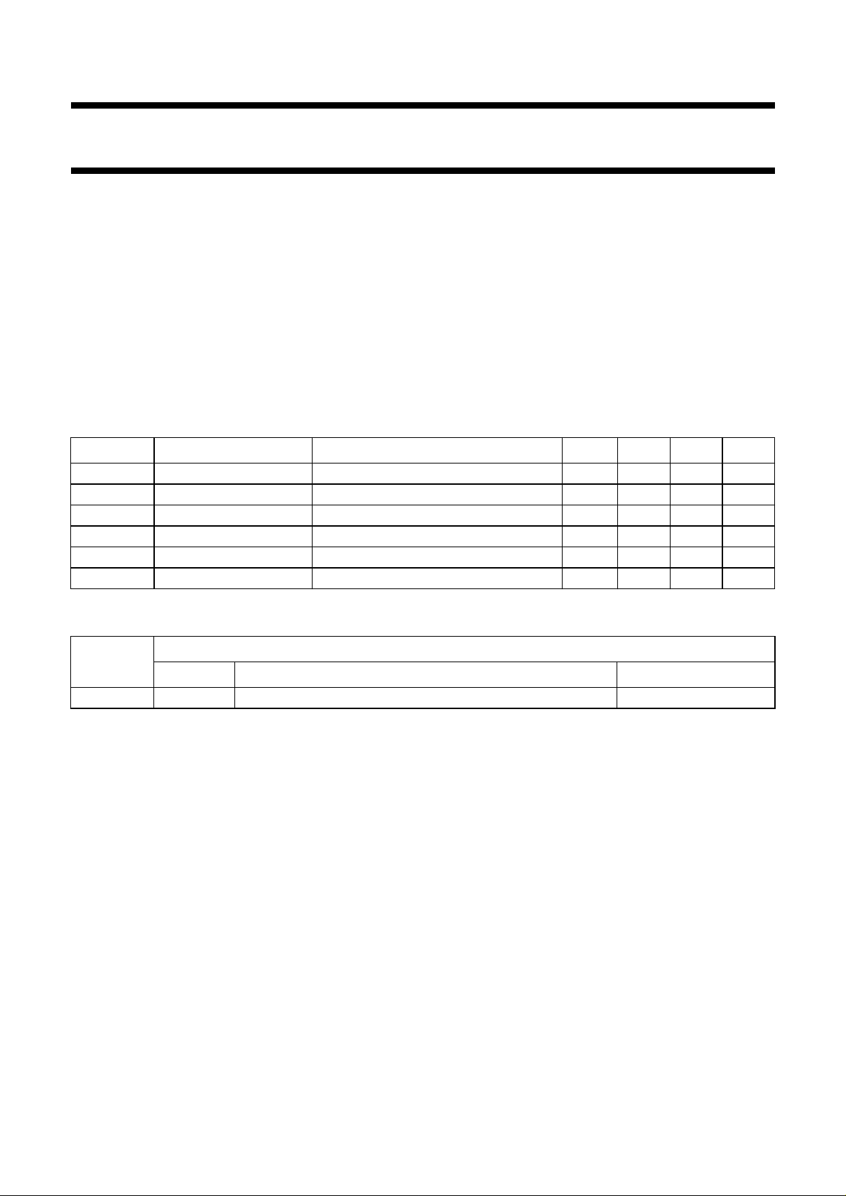
BLOCK DIAGRAM
PINNING
SYMBOL PIN DESCRIPTION
V
CC
IFI1 2 IF input 1
IFI2 3 IF input 2
V
CC
IFO1 5 IF output 1
AGC 6 AGC input
GND 7 ground
IFO2 8 IF output 2
1 supply voltage
4 supply voltage
Fig.1 Block diagram.
Fig.2 Pin configuration.
February 1995 3
Philips Semiconductors Product specification
IF amplifier for satellite TV receivers TDA8011T
LIMITING VALUES
In accordance with the Absolute Maximum Rating System (IEC 134).
SYMBOL PARAMETER MIN. MAX. UNIT
V
CC
V
(max)
I
source(max)
t
sc(max)
T
stg
T
j
T
amb
THERMAL CHARACTERISTICS
SYMBOL PARAMETER VALUE UNIT
R
th j-a
supply voltage −0.3 6.0 V
maximum voltage on all pins −0.3 V
CC
V
maximum output source current − 10 mA
maximum short-circuit time on outputs − 10 s
storage temperature −55 +150 °C
junction temperature − +150 °C
operating ambient temperature −10 +80 °C
thermal resistance from junction to ambient in free air 160 K/W
HANDLING
Inputs and outputs are protected against electrostatic discharge in normal handling. However, to be totally safe it is
desirable to take normal precautions appropriate to handling MOS devices.
CHARACTERISTICS
=5V; fi= 70, 480 and 610 MHz; T
V
CC
=25°C; measured in application circuit of Fig.6; unless otherwise specified.
amb
SYMBOL PARAMETER CONDITIONS MIN. TYP. MAX. UNIT
Supply
I
CC
supply current 27 35 45 mA
IF amplifier
G
v(max)
G
v(min)
∆G tilt ∆f
V
i
V
I(DC)
V
o
V
O(DC)
F noise figure unmatched configuration;
maximum voltage gain V
minimum voltage gain V
= 0.9VCC; note 1 25 −−dB
AGC
= 0.1VCC; note 1 −−−21 dB
AGC
= 20 MHz; note 2 − 0.4 − dB
i
input voltage level −−96 dBµV
DC input voltage level − 2.5 − V
output voltage level −−85 dBµV
DC output voltage level − 2.2 − V
−−15 dB
note 3
F
(min)
IM3 third-order intermodulation
minimum noise figure note 4 −−11 dB
note 5 − 40 − dB
distance
R
C
R
i(diff)
i(diff)
o(SE)
differential input resistance note 6 − 4 − kΩ
differential input capacitance note 6 − 0.75 − pF
single-ended output resistance − 50 −Ω
February 1995 4
 Loading...