

Philips TDA8008 Datasheet

INTEGRATED CIRCUITS
DATA SH EET
TDA8008
Dual multiprotocol smart card
coupler
Objective specification
File under Integrated Circuits, IC02
1999 Dec 14

Philips Semiconductors Objective specification
Dual multiprotocol smart card coupler TDA8008
FEATURES
• 8xC51 core with 16 kbytes or EPROM (TDA8008),
256 bytes RAM, 512 bytesAUXRAM, Timer 0, 1, 2 and
enhanced UART
• Specific ISO 7816 UART, accessible with MOVX
instructions for automatic convention processing,
variable baud rate through frequency or division ratio
programming, error management at character level for
T = 0 protocol, extra guard time register
• Dual VCC generation (5 V ±5% or 3 V ±5%), maximum
current of 60 mA with controlled rise and fall times
• Dual cards clock generation (up to 10 MHz) with two
times synchronous frequency doubling
• Cards clock STOP HIGH or LOW or 1.25 MHz (from an
integrated oscillator) for cards power reduction mode
• Automatic activation and deactivation sequences
through an independent sequencer
• Supports the asynchronous protocols T = 0 and T = 1 in
accordance with ISO 7816 and EMV
• Versatile 24-bit time-out counter for Answer To Reset
(ATR) and waiting times processing
• 22 ETU counter for block guard time
• Supports synchronous cards
• Current limitations on cards contacts
• Special circuitry for killing spikes during power-on or off
• Supply supervisor for Power-on reset
• Step-up converter (supply voltage from 2.7 to 5.5 V at
16 MHz), doubler, tripler or follower according to V
and V
DD
CC
• Speed up to 25 MHz at VDD=5V
• Additional I/O pin allowing the use of the ISO 7816
UART for an external card interface (pin IOAUX)
• Additional interrupt pin allowing detection of level
toggling on an external signal (pin INTAUX)
• Fast and efficient swapping between the 3 cards due to
separate buffering of parameters for each card
• Chip select input allowing use of several devices in
parallel and memory space paging
• Enhanced ESD protections on card contacts (6 kV min.)
• Software library for easy integration within the
application
• Development tool with a TDA8007B and a regular
emulator.
APPLICATIONS
• Multiple smart card readers for multiprotocol
applications (EMV banking, digital pay TV, access
control, etc.).
GENERAL DESCRIPTION
TheTDA8008 is a complete, one-chip,low cost dual smart
card coupler.
Itcanbeusedas the kernel of a multiple card reader. It can
handle all ISO 7816, EMV and GSM11-11 requirements.
The integrated ISO 7816 UART and the time-out counters
allow easy use even at high baud rates with no real time
constraints. Due to its chip select and external I/O and
interrupt features, it simplifies the realization of any
number of cards reader. It gives the cards and the set a
very high level of security, due to its special hardware
against ESD, short-circuiting, power failure and
overheating. Its integrated step-up converter allows
operation within a supply voltage range of 2.7 to 5.5 V at
16 MHz.
The OTP version of the TDA8008 allows fast and reliable
software development and fast product introduction.
A software library has been developed, that can handle all
actions required for T = 0, T = 1 and synchronous
protocols.
ORDERING INFORMATION
PACKAGE
TYPE NUMBER
NAME DESCRIPTION VERSION
TDA8008HL LQFP80 plastic low profile quad flat package; 80 leads; body 12 × 12 × 1.4 mm SOT315-1
1999 Dec 14 2
Philips Semiconductors Objective specification
Dual multiprotocol smart card coupler TDA8008
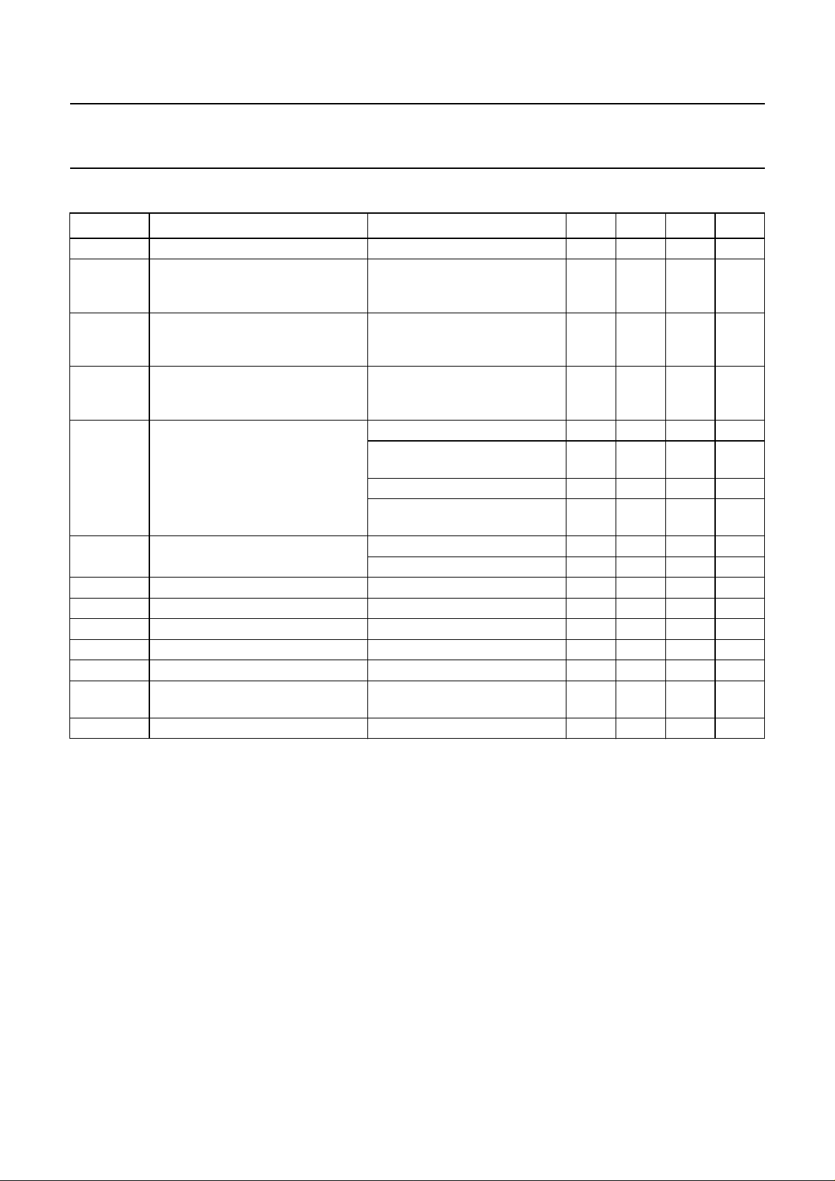
QUICK REFERENCE DATA
SYMBOL PARAMETER CONDITIONS MIN. TYP. MAX. UNIT
V
DD
I
DD(pd)
I
DD(sm)
I
DD(om)
V
CC
I
CC
I
CC1+ICC2
SR slew rate on V
t
de
t
act
f
XTAL
f
op
T
amb
supply voltage V
DDD=VDDA=VDDP
supply current in Power-down mode VDD= 3.3 V; cards inactive;
2.7 − 5.5 V
−−tbf µA
8xC51 controller in power-down
mode; note 1
supply current in sleep mode VDD= 3.3 V; cards active at
−−tbf mA
VCC= 5V;clockstopped; 8xC51
controller in Idle mode; note 1
supply current in operating mode VDD= 3.3 V; f
V
CC1=VCC2
I
CC1+ICC2
= 80 mA; note 1
XTAL1
=5V;
= 20 MHz
−−tbf mA
card output supply voltage including static loads (5 V card) 4.75 5.0 5.25 V
with 40 nAs dynamic loads on
4.6 5.0 5.4 V
200 nF capacitor (5 V card)
including static loads (3 V card) 2.80 3.0 3.20 V
with 40 nAs dynamic loads on
2.75 3.0 3.25 V
200 nF capacitor (3 V card)
card output supply current operating −−65 mA
overload detection − 80 − mA
sum of both cards currents −−80 mA
(rise and fall) CL= 300 nF (max.) 0.10 0.16 0.22 V/µs
CC
deactivation cycle duration −−100 µs
activation cycle duration −−225 µs
crystal frequency 3.5 − 25 MHz
operating frequency external frequency applied to
0 − 25 MHz
pin XTAL1
ambient temperature −25 − +85 °C
Note
in all configurations includes the current at pins V
1. I
DD
DDD
1999 Dec 14 3
, V
DDA
and V
DDP
.
Philips Semiconductors Objective specification
Dual multiprotocol smart card coupler TDA8008
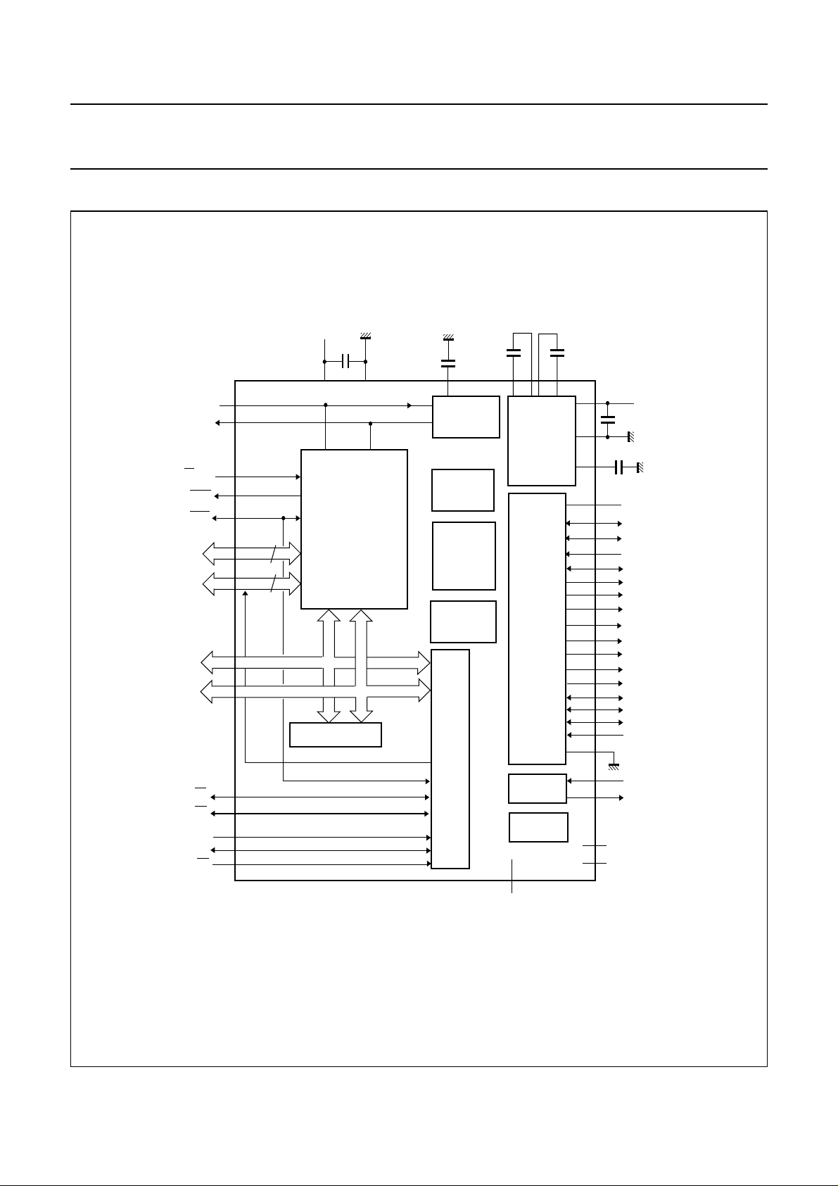
BLOCK DIAGRAM
handbook, full pagewidth
SBP
SAP
25 16
200 nF
SAM
17
23
V
DDP
GNDP
RESET
RSTOUT
DDD
V
3
39
51
GNDD
52
200 nF
CDELAY
6
SUPPLY
SUPERVISOR
SBM
24
18
STEP-UP
CONVERTER
EA/VPP
PSEN
ALE/PROG
P10 to P17
P30 to P37
P20 to P27
P00 to P07
P36/WR
P37/RD
INTAUX
IOAUX
CS
65
63
64
75 to 80,
1, 2
41 to 48
53 to 62
67 to 74
47
48
35
37
38
8xC51 CONTROLLER
16 KBYTES ROM or OTP
256 BYTES RAM
TIMER 0, 1 and 2
8
8
ENHANCED UART
512 BYTES AUXRAM
BY MOVX
TDA8008
ALE
TIME-OUT
COUNTER
ISO 7816
UART
CLOCK
CIRCUITRY
INTERFACE CONTROL
ANALOG
DRIVERS
AND
SEQUENCER
XTAL
OSCILLATOR
INTERNAL
OSCILLATOR
19 to 22, 40,
58, 59, 66
n.c.
26
4
34
33
32
31
30
29
28
27
15
14
13
12
11
10
9
8
5
50
49
36
7
FCE568
200 nF
V
I/01
C81
PRES1
C41
RST1
V
CLK1
GNDC1
GNDC2
CLK2
V
RST2
C42
C82
I/02
PRES2
GNDA
XTAL1
XTAL2
TEST
INHIB
VUP
DDA
CC1
CC2
Fig.1 Block diagram.
1999 Dec 14 4
 Loading...