

Philips TDA8001T-C1, TDA8001AT-C1, TDA8001A-C1, TDA8001-C1 Datasheet

DATA SH EET
Product specification
Supersedes data of 1995 Feb 01
File under Integrated Circuits, IC02
1996 Dec 12
INTEGRATED CIRCUITS
TDA8001
Smart card interface

1996 Dec 12 2
Philips Semiconductors Product specification
Smart card interface TDA8001
FEATURES
• Protected I/O line
• VCC regulation (5 V ±5%, 100 mA max. with controlled
rise and fall times)
• VPP generation (12.5, 15 or 21 V ±2.5%, 50 mA max.,
with controlled rise and fall times) (only at TDA8001 and
TDA8001T)
• Clock generation (up to 10 MHz), with synchronous
frequency doubling
• Overload, thermal and card extraction protections
• Current limitation in case of short-circuit
• Idle mode and special circuitry for spikes killing during
powering on and off
• Two voltage supervisors (digital and analog supplies)
• Automatic activation and deactivation sequences
through an independent internal clock
• Enhanced ESD protections on card side (4 kV min.)
• Easy chaining for multiple card readers
• ISO 7816 compatibility.
APPLICATIONS
• Pay TV (multistandards conditional access system,
videoguard, newscript)
• Multi-application smart card readers (banking, vending
machine, electronic payment identification).
GENERAL DESCRIPTION
The TDA8001 is a complete, low-cost analog interface
which can be positioned between an asynchronous smart
card (ISO 7816) and a microcontroller. It is directly
compatible with the new Datacom chip verifier.
The complete supply, protection and control functions are
realized with only a few external components, making this
product very attractive for consumer applications
(see Chapter “Application information”).
ORDERING INFORMATION
TYPE
NUMBER
PACKAGE
NAME DESCRIPTION VERSION
TDA8001;
TDA8001A
DIP28 plastic dual in-line package; 28 leads (600 mil) SOT117-1
TDA8001T;
TDA8001AT
SO28 plastic small outline package; 28 leads; body width 7.5 mm SOT136-1
1996 Dec 12 3
Philips Semiconductors Product specification
Smart card interface TDA8001
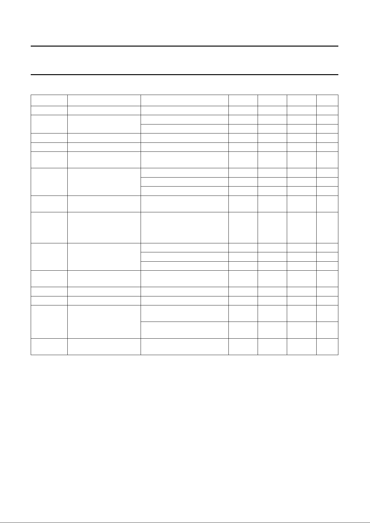
QUICK REFERENCE DATA
SYMBOL PARAMETER CONDITIONS MIN. TYP. MAX. UNIT
V
DD
supply voltage 6.7 − 18 V
I
DD
supply current idle mode; VDD=12V − 32 − mA
active modes; unloaded − 45 − mA
V
th2
threshold voltage on V
SUP
4.5 − 4.72 V
V
th4
threshold voltage on V
DD
6 − 6.5 V
V
CC
card supply voltage including static and dynamic
loads on 100 nF capacitor
4.75 5.0 5.25 V
I
CC
card supply current operating −−−100 mA
detection −−150 − mA
limitation −−−200 mA
V
H
high voltage supply for
V
PP
−−30 V
V
PP
card programming
voltage (only at TDA8001
and TDA8001T)
(P = 5, 12.5, 15 and 21 V)
including static and dynamic
loads on 100 nF capacitor
P − 2.5% − P + 2.5% V
I
PP
programming current
(read or write mode)
operating −−−50 mA
detection −−75 − mA
limitation −−−100 mA
SR slew rate on V
CC
and V
PP
(rise and fall)
maximum load capacitor 150 nF − 0.38 − V/µs
t
de
deactivation cycle duration 75 100 125 µs
f
clk
clock frequency 0 − 8 MHz
P
tot
continuous total power
dissipation
TDA8001; T
amb
= +70 °C;
see Fig.10
−−0.92 W
TDA8001T; T
amb
= +70 °C;
see Fig.11
−−2W
T
amb
operating ambient
temperature
0 − +70 °C
1996 Dec 12 4
Philips Semiconductors Product specification
Smart card interface TDA8001
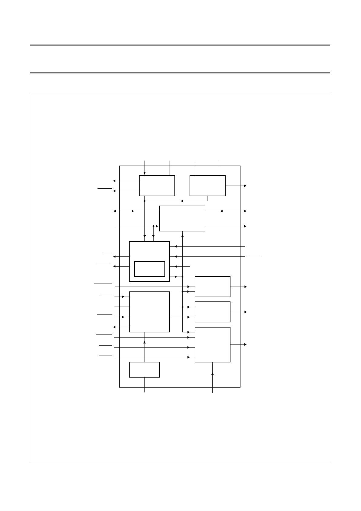
BLOCK DIAGRAM
Fig.1 Block diagram.
handbook, full pagewidth
MBH813
PROTECTIONS
AND
ENABLE
MAIN
SUPPLY
VOLTAGE
SUPERVISOR
INTERNAL
CLOCK
LOGIC
V
CC
GENERATOR
CLOCK
ENABLE
CLOCK
CIRCUITRY
23
24
2
20
19
26
28
18
17
15 16 13 12
6
7
111
14
8
9
4
22
3
V
PP
GENERATOR
10
5
OSCILLATOR
PROTECTIONS
XTAL
I/O
RST
CLK
VPP12.5
VPP15
21
VPP21
PRES
PRES
V
PP
V
DD
V
CC
V
H
GND1
I/O(µC)
RSTIN
CMD3.5
GND2
CVNC
27
25
CMDVCC
CLKOUT2
CMD7
DETECT
OFF
ALARM
ALARM
DELAY
V
SUP
TDA8001
1996 Dec 12 5
Philips Semiconductors Product specification
Smart card interface TDA8001
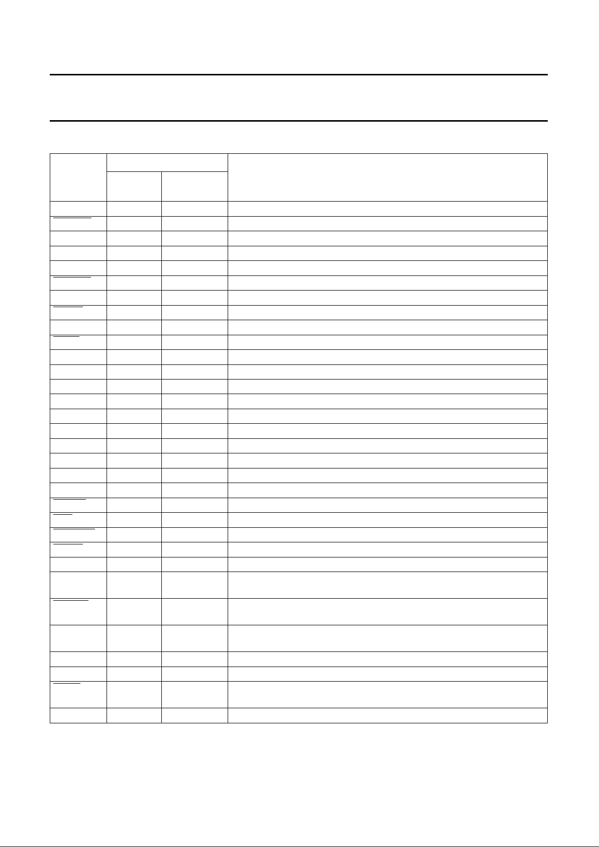
PINNING
SYMBOL
PIN
DESCRIPTION
TDA8001
TDA8001T
TDA8001A
TDA8001AT
XTAL 1 1 crystal connection
DETECT 2 2 card extraction open collector output (active LOW)
I/O 3 3 data line to/from the card
RST 4 4 card reset output
CLK 5 5 clock output to the card
VPP12.5 6 − control input for applying the 12.5 V programming voltage (active LOW)
n.c. − 6 not connected
VPP15 7 − control input for applying the 15 V programming voltage (active LOW)
n.c. − 7 not connected
PRES 8 8 card presence contact input (active LOW)
PRES 9 9 card presence contact input (active HIGH)
V
PP
10 − card programming voltage output
n.c. − 10 not connected
V
H
11 11 HIGH voltage supply for VPP generation
GND1 12 12 ground 1
V
DD
13 13 positive supply voltage
V
CC
14 14 card supply output voltage
V
SUP
15 15 voltage supervisor input
DELAY 16 16 external capacitor connection for delayed reset timing
ALARM 17 17 open-collector reset output for the microcontroller (active HIGH)
ALARM 18 18 open-collector reset output for the microcontroller (active LOW)
OFF 19 19 open-collector interrupt output to the microcontroller (active LOW)
CMDVCC 20 20 control input for applying supply voltage to the card (active LOW)
VPP21 21 − control input for applying the 21 V programming voltage (active LOW)
n.c. − 21 not connected
CVNC 22 22 internally generated 5 V reference, present when V
DD
is on; to be
decoupled externally (100 nF)
CMD3.5
or CDMTC
23 23 control input for having the crystal frequency divided-by-4 at pin CLK
CLKOUT2 24 24 clock output to the microcontroller, or any other R4590
(crystal frequency divided by two)
GND2 25 25 ground 2
RSTIN 26 26 card reset input from the microcontroller (active HIGH)
CMD7
or CDMS
27 27 control input for having the crystal frequency divided by 2 at pin CLK
I/O(µC) 28 28 data line to/from the microcontroller
1996 Dec 12 6
Philips Semiconductors Product specification
Smart card interface TDA8001
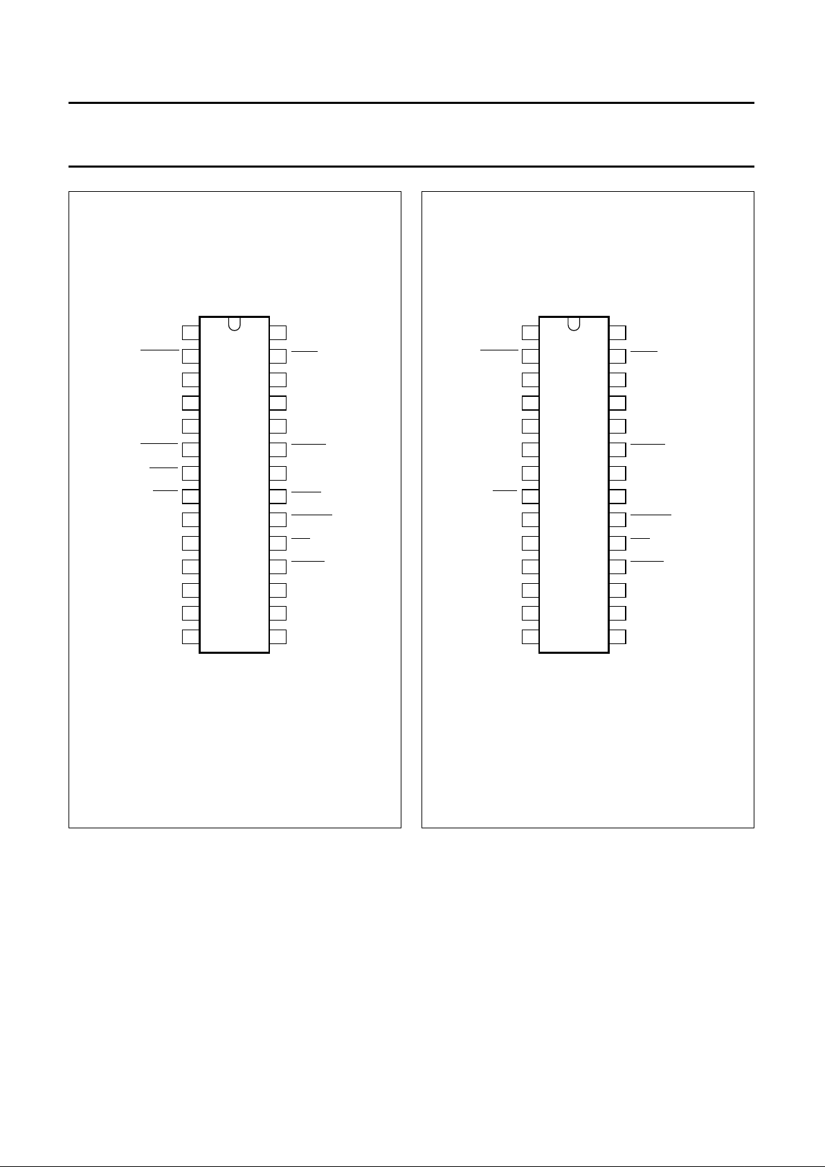
Fig.2 Pin configuration.
handbook, halfpage
TDA8001
TDA8001T
MBH811
1
2
3
4
5
6
7
8
9
10
11
12
13
14
28
27
26
25
24
23
22
21
20
19
18
17
16
15
XTAL
DETECT
I/O
RST
CLK
VPP12.5
VPP15
PRES
PRES
V
PP
V
DD
V
CC
V
H
GND1
I/O(µC)
CMD7 or CDMS
RSTIN
GND2
CLKOUT2
CMD3.5 or CDMTC
CVNC
VPP21
CMDVCC
OFF
ALARM
ALARM
DELAY
V
SUP
Fig.3 Pin configuration.
handbook, halfpage
TDA8001A
TDA8001AT
MBH812
1
2
3
4
5
6
7
8
9
10
11
12
13
14
28
27
26
25
24
23
22
21
20
19
18
17
16
15
XTAL
DETECT
I/O
RST
CLK
n.c.
n.c.
PRES
PRES
n.c.
V
DD
V
CC
V
H
GND1
I/O(µC)
CMD7 or CDMS
RSTIN
GND2
CLKOUT2
CMD3.5 or CDMTC
CVNC
n.c.
CMDVCC
OFF
ALARM
ALARM
DELAY
V
SUP

1996 Dec 12 7
Philips Semiconductors Product specification
Smart card interface TDA8001
FUNCTIONAL DESCRIPTION
Power supply
The circuit operates within a supply voltage range of
6.7 to 18 V. V
DD
and GND are the supply pins. All card
contacts remain inactive during power up or down.
P
OWER UP
The logic part is powered first and is in the reset condition
until VDD reaches V
th1
. The sequencer is blocked until V
DD
reaches V
th4+Vhys4
.
P
OWER DOWN
When VDD falls below V
th4
, an automatic deactivation of
the contacts is performed.
Voltage supervisor
This block surveys the 5 V supply of the microcontroller
(V
SUP
) in order to deliver a defined reset pulse and to avoid
any transients on card contacts during power up or down
of V
SUP
. The voltage supervisor remains active even if V
DD
is powered-down.
P
OWER ON
As long as V
SUP
is below V
th2+Vhys2
the capacitor C
DEL
,
connected to pin DELAY, will be discharged. When V
SUP
rises to the threshold level, C
DEL
will be recharged.
ALARM and ALARM remain active, and the sequencer is
blocked until the voltage on the DELAY line reaches V
th3
.
P
OWER DOWN (see Fig.4)
If V
SUP
falls below V
th2
, C
DEL
will be discharged, ALARM
andALARM become active, and an automatic deactivation
of the contacts is performed.
Clock circuitry (see Fig.5)
The clock signal (CLK) can be applied to the card in two
different methods:
1. Generation by a crystal oscillator: the crystal, or the
ceramic resonator (4 to 16 MHz) is connected to the
XTAL pin.
2. Use of a signal frequency (up to 20 MHz), already
present in the system and connected to the XTAL pin
via a 10 nF capacitor (see Fig.14). In both cases the
frequency is first divided-by-two.
If
CMD7 (respectively CMD3.5) is LOW, the clock signal
(its frequency again divided by two) is enabled and
buffered before being fed to the CLK pin.
CMD3.5 and internal ENRST are sampled in order to give
the first clock pulse the correct width, and to avoid false
pulses during frequency change.
The CLKOUT2 pins may be used to clock a
microcontroller or an other TDA8001. The signal1⁄2f
xtal
is
available when the circuit is powered up.
State diagram
Once activated, the circuit has six possible modes of
operation:
• Idle
• Activation
• Read
• Write
• Deactivation
• Fault.
Figure 6 shows the way these modes are accessible.
I
DLE MODE
After reset, the circuit enters the IDLE state. A minimum
number of circuits are active while waiting for the
microcontroller to start a session.
• All card contacts are inactive
• I/O(µC) is high impedance
• Voltage generators are stopped
• Oscillator or XTAL input is running, delivering CLKOUT2
• Voltage supervisors are active.
The DETECT line is HIGH if a card is present (PRES and
PRES active) and LOW if a card is not present. The OFF
line is HIGH if no hardware problem is detected.
A
CTIVATION SEQUENCE
From the IDLE mode, the circuit enters the ACTIVATION
mode when the microcontroller sets the CMDVCC line
(active LOW). The I/O(µC) signal must not be LOW.
The internal circuitry is activated, the internal clock starts
and the sequence according to ISO7816 is performed:
• VCC rises from 0 to 5 V
• VPP rises from 0 to 5 V and I/O is enabled
• CLK and RST are enabled.
The time interval between steps 1 and 2 is 16 µs, and
64 µs between steps 2 and 3 (see Fig.7).

1996 Dec 12 8
Philips Semiconductors Product specification
Smart card interface TDA8001
READ MODE
When the activation sequence is completed and, after the
card has replied its Answer-to-Reset, the TDA8001 will be
in the READ mode. Data is exchanged between the card
and the microcontroller via the I/O line.
W
RITE MODE
Cards with EPROM memory need a programming voltage
(VPP). When it is required to write to the internal memory
of the card, the microcontroller sets one of the VPP12.5,
VPP15 and VPP21 lines LOW, according to the
programming value given in the Answer-to-Reset.
VPP rises from 5 V to the selected value with a typical slew
rate of 0.38 V/µs. In order to respect the ISO 7816 slopes,
the circuit generates VPP by charging and discharging an
internal capacitor. The voltage on this capacitor is then
amplified by a power stage gain of 5, powered via an
external supply pin VH (30 V max).
D
EACTIVATION SEQUENCE (see Fig.8)
When the session is completed, the microcontroller sets
the CMDVCC line to its HIGH state. The circuit then
executes an automatic deactivation sequence by counting
the sequencer back:
• RST falls to LOW and CLK is stopped
• I/O(µC) becomes high impedance and VPP falls to 0 V
• VCC falls to 0 V.
The circuit returns to the IDLE mode on the next rising
edge of the clock.
P
ROTECTIONS
Main fault conditions are monitored by the circuit:
• Short-circuit or overcurrent on V
CC
• Short-circuit or overcurrent on V
PP
• Card extraction during transaction
• Overheating problem
• V
SUP
drop-out
• VDD drop-out.
When one of these fault conditions is detected, the circuit
pulls the interrupt line
OFF to its active LOW state and
returns to the FAULT mode. The current on I/O is internally
limited to 5 mA.
F
AULT MODE (see Fig.9)
When a fault condition is written to the microcontroller via
the OFF line, the circuit initiates a deactivation sequence.
After the deactivation sequence has been completed, the
OFF line is reset to its HIGH state after the microcontroller
has reset the CMDVCC line HIGH.
Fig.4 Alarm and delay as a function of V
SUP
(C
DEL
fixes the pulse width).
handbook, full pagewidth
MGG818
V
SUP
V
th2
+ V
hys2
V
th2
V
th3
t
d
V
DELAY
ALARM
 Loading...