

Philips TDA8000T Datasheet
INTEGRATED CIRCUITS
DATA SH EET
TDA8000; TDA8000T
Smart card interface
Product specification
Supersedes data of 1995 Feb 01
File under Integrated Circuits, IC02
1996 Dec 12
Philips Semiconductors Product specification
Smart card interface TDA8000; TDA8000T
FEATURES
• Two protected I/O lines
• VCC regulation (5 V ±4%, 100 mA max. with controlled
rise and fall times)
• VPP generation (12.5, 15 or 21 V ±2.5%, 50 mA max.
APPLICATIONS
• Pay TV
• Telematics
• Cashless payment
• Multipurpose card-readers, etc.
programmable by two bits, with controlled rise and fall
times)
• Clock generation (up to 8 MHz)
• Short-circuit, thermal and card extraction protections
• Two voltage supervisors (digital and analog supplies)
• Automatic activation and deactivation sequences via an
independent internal clock
• Enhanced ESD protections on card connections
(4 kV min.)
• ISO 7816 approval.
GENERAL DESCRIPTION
The TDA8000 is a complete, low-cost analog interface
which can be positioned between a smart card or a
memory card (ISO 7816) and a microcontroller. It is
approved for banking, telecom and pay TV applications.
The complete supply, protection and control functions are
realized with only a few external components, which
makes the TDA8000 very attractive for consumer
applications. Application suggestions and support is
available on request (see examples in
Chapter “Application information”).
QUICK REFERENCE DATA
SYMBOL PARAMETER CONDITIONS MIN. TYP. MAX. UNIT
V
DD
I
DD
supply voltage 6.7 − 18 V
supply current idle mode; VDD=12V − 25 − mA
active modes; unloaded − 32 − mA
V
th2
V
CC
I
CC
V
H
I
PP
, t
t
de
act
threshold voltage on V
SUP
card supply voltage 4.8 5.0 5.2 V
card supply current −−−100 mA
high voltage supply for V
PP
programming current read mode; VPP=5V −−−50 mA
write mode; V
>5V −−−50 mA
PP
deactivation/activation cycle
4.5 − 4.68 V
−−30 V
−−500 µs
duration
P
tot
continuous total power
dissipation
TDA8000; T
see Fig.10
TDA8000T; T
amb
amb
= +70 °C;
= +70 °C;
−−2W
−−0.92 W
see Fig.11
T
amb
operating ambient temperature 0 − +70 °C
ORDERING INFORMATION
TYPE
NUMBER
NAME DESCRIPTION VERSION
PACKAGE
TDA8000 DIP28 plastic dual in-line package; 28 leads (600 mil) SOT117-1
TDA8000T SO28 plastic small outline package; 28 leads; body width 7.5 mm SOT136-1
1996 Dec 12 2
Philips Semiconductors Product specification
Smart card interface TDA8000; TDA8000T
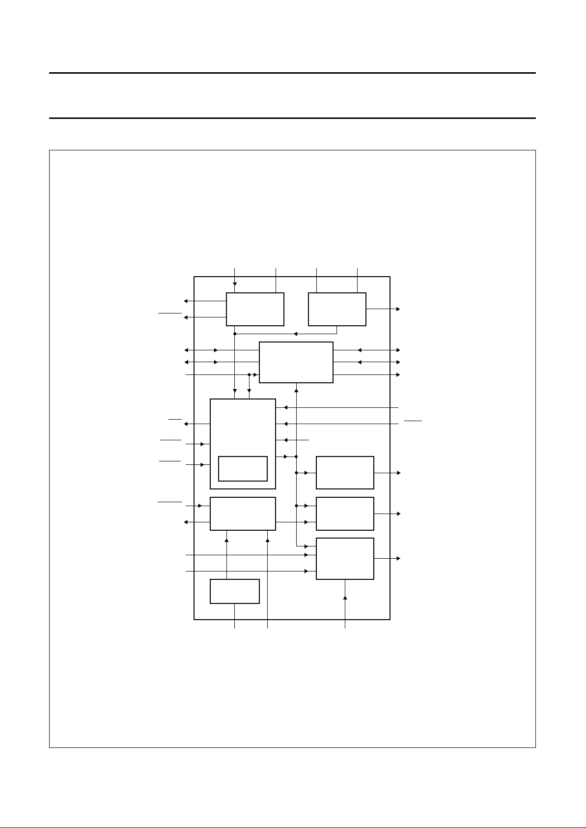
BLOCK DIAGRAM
handbook, full pagewidth
ALARM
ALARM
I/O1(µC)
I/O2(µC)
RSTIN
OFF
START
WRITE
CLKDIV
CLKOUT
17
18
28
27
26
19
20
21
23
25
AND
ENABLE
V
DD
MAIN
SUPPLY
V
SUP
SUPERVISOR
DELAY
15 16 13 12
VOLTAGE
PROTECTIONS
TDA8000
LOGIC
PROTECTIONS
INTERNAL
CLOCK
CLOCK
CIRCUITRY
GENERATOR
ENABLE
V
CC
CLOCK
GND
22
CVNC
3
I/O1
2
I/O2
4
RST
9
PRES
8
PRES
14
V
CC
5
CLK
PSEL1
PSEL2
6
7
OSCILLATOR
124 11
XTAL
CLKIN
Fig.1 Block diagram.
1996 Dec 12 3
V
PP
GENERATOR
V
H
10
MBH810
V
PP
Philips Semiconductors Product specification
Smart card interface TDA8000; TDA8000T
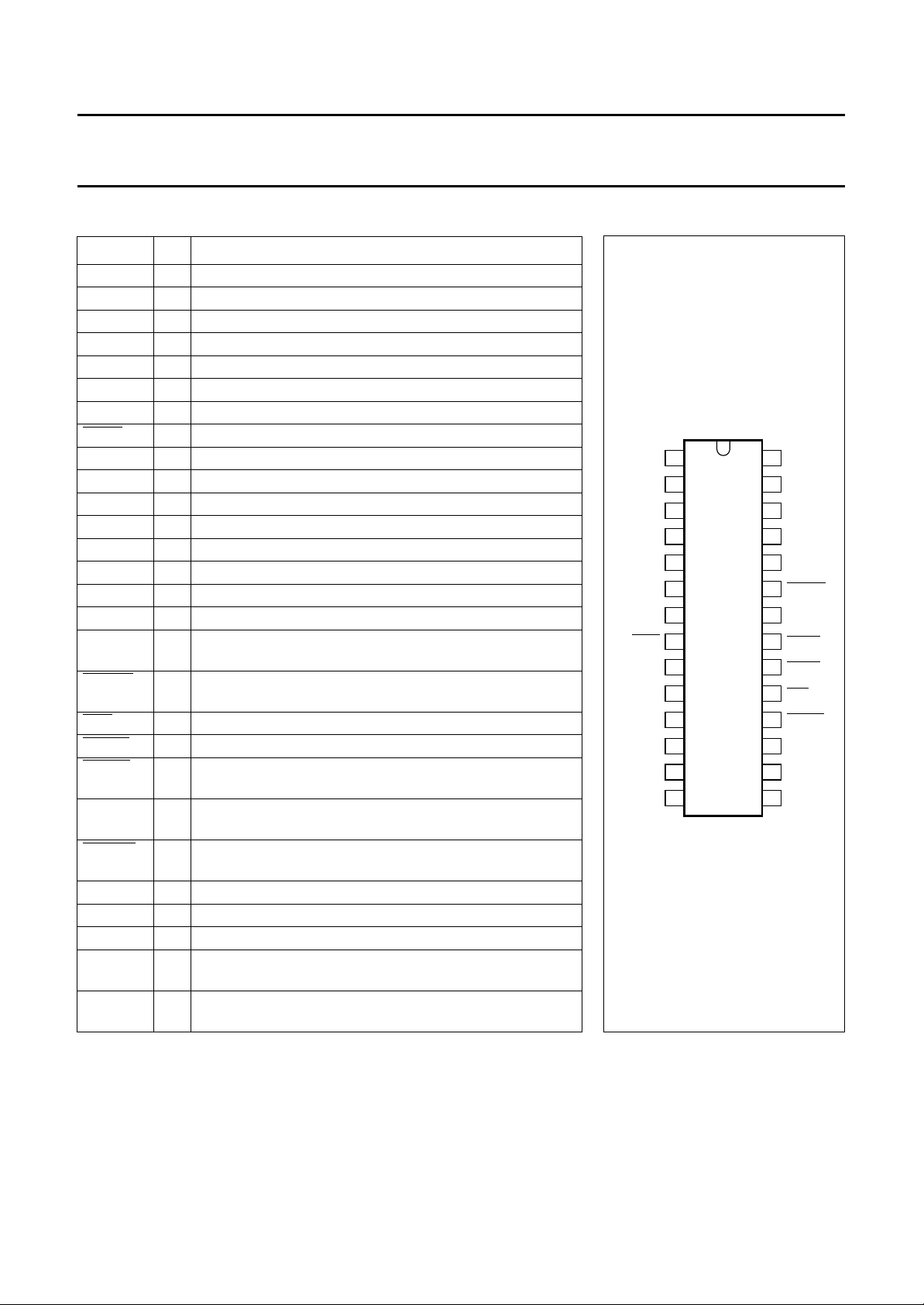
PINNING
SYMBOL PIN DESCRIPTION
XTAL 1 crystal connection
I/O2 2 data line to/from the card
I/O1 3 data line to/from the card
RST 4 card reset output
CLK 5 clock output to the card
PSEL1 6 programming voltage selection input (see Table 1)
PSEL2 7 programming voltage selection input (see Table 1)
PRES 8 card presence contact input (active LOW)
PRES 9 card presence contact input (active HIGH)
V
PP
V
H
10 card programming voltage output
11 high voltage supply for VPP generation
GND 12 ground
V
V
V
DD
CC
SUP
13 positive supply voltage
14 card supply output voltage
15 voltage supervisor input
DELAY 16 external capacitor connection for delayed reset timing
ALARM 17 open-collector reset output for the microcontroller (active
HIGH)
ALARM 18 open-collector reset output for the microcontroller (active
LOW)
OFF 19 interrupt output to the microcontroller (active LOW)
START 20 microcontroller input for starting session (active LOW)
WRITE 21 control input for applying programming voltage to the card
(active LOW)
CVNC 22 internally generated 5 V reference, present when V
DD
is
on; to be decoupled externally (47 nF)
CLKDIV 23 input for dividing/not dividing the CLKOUT frequency by
two (active LOW)
CLKIN 24 external clock signal input
CLKOUT 25 clock output to the microcontroller, or another TDA8000
RSTIN 26 card reset input from the microcontroller (active HIGH)
I/O2(µC) 27 data line to/from the microcontroller; must not be left
open-circuit, tie to CVNC if not used
I/O1(µC) 28 data line to/from the microcontroller; must not be left
open-circuit, tie to CVNC if not used
page
XTAL
I/O2
I/O1
RST
CLK
PSEL1
PSEL2
PRES
PRES
V
PP
V
GND
V
DD
V
CC
H
1
2
3
4
5
6
7
TDA8000T
8
9
10
11
12
13
14
TDA8000
Fig.2 Pin configuration.
MBH809
28
27
26
25
24
23
22
21
20
19
18
17
16
15
I/O1(µC)
I/O2(µC)
RSTIN
CLKOUT
CLKIN
CLKDIV
CVNC
WRITE
START
OFF
ALARM
ALARM
DELAY
V
SUP
1996 Dec 12 4

Philips Semiconductors Product specification
Smart card interface TDA8000; TDA8000T
FUNCTIONAL DESCRIPTION
Power supply
The circuit operates within a supply voltage range of
6.7 to 18 V. V
and GND are the supply pins. All card
DD
contacts remain inactive during power-up or power-down,
provided VDD does not rise or fall too fast (0.5 V/ms typ.).
P
OWER-UP
The logic part is powered first and is in the reset condition
until VDD reaches V
reaches V
OWER-DOWN
P
th4+Vhys4
When VDD falls below V
. The sequencer is blocked until V
th1
.
, an automatic deactivation of
th4
DD
the contacts is performed.
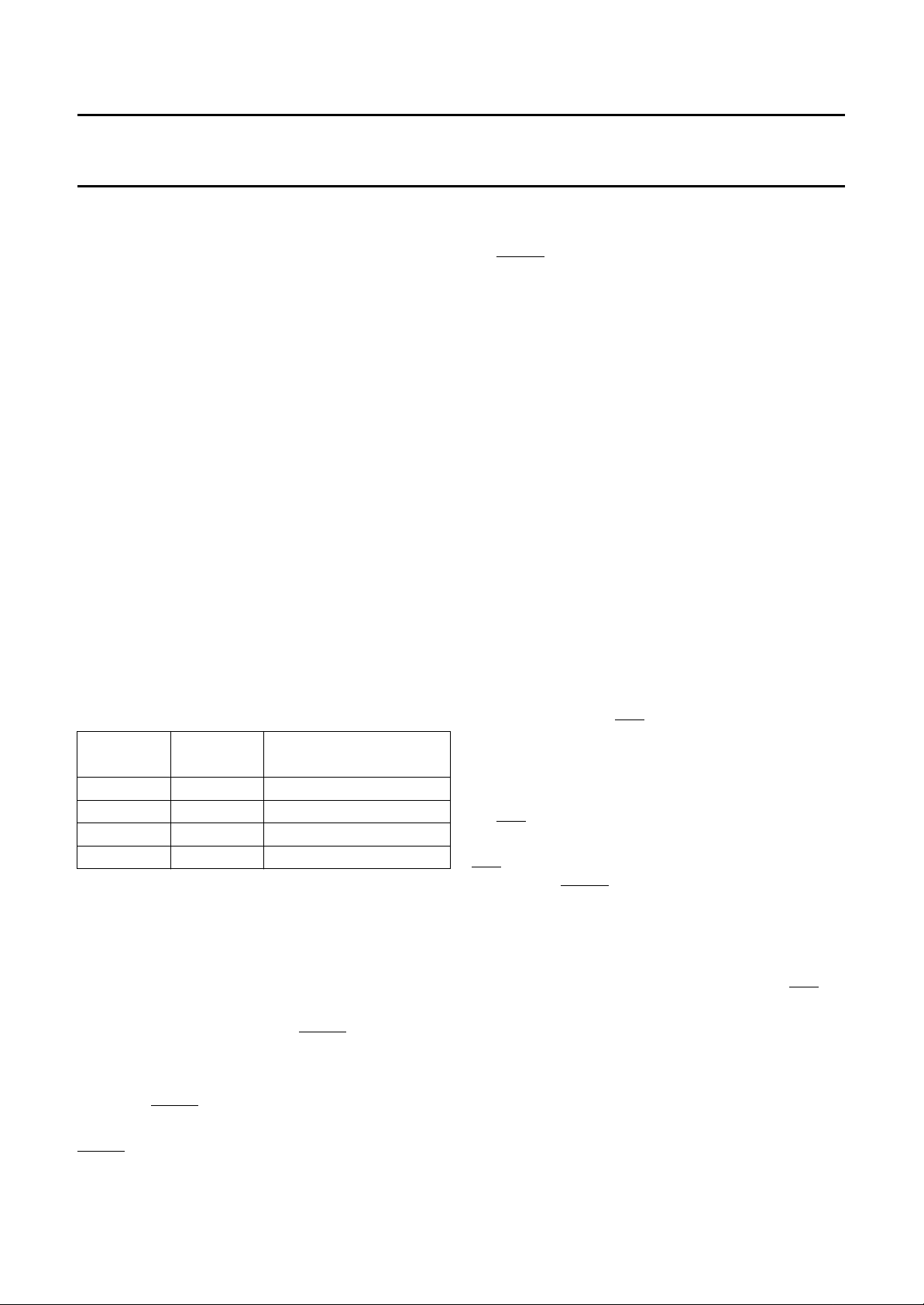
Voltage supervisor
This block surveys the 5 V supply of the microcontroller
) in order to deliver a defined reset pulse and to avoid
(V
SUP
any transients on card contacts during power-up or
power-down of V
SUP
.
The voltage supervisor remains active even if VDD is
powered-down.
OWER-UP
P
As long as V
is below V
SUP
th2+Vhys2
the capacitor C
DEL
connected to the pin DELAY, will be discharged. When
V
rises to the threshold level, C
SUP
will be recharged.
DEL
ALARM and ALARM remain active, and the sequencer is
blocked until the voltage on the pin DELAY reaches V
OWER-DOWN (see Fig.3)
P
If V
falls below V
SUP
th2
, C
will be discharged, ALARM
DEL
th3
andALARM become active, and an automatic deactivation
of the contacts is performed.
Clock circuitry (see Fig.4)
The clock signal (CLK) can be applied to the card by two
different methods:
1. Generation by a crystal oscillator: the crystal
(3 to 11 MHz) is connected to pin XTAL. Its frequency
is divided by two.
2. Use of a signal frequency already present in the
system and connected to the pin CLKIN (up to 8 MHz).
Pin XTAL has to be connected to GND via a 1 kΩ
resistor. In this event, the CLKOUT signal remains
LOW.
In both events the signal is buffered and enabled.
Pin CLKOUT may be used to clock a microcontroller.
The signal (
1
⁄2f
or f
xtal
if CLKDIV is HIGH) is available
xtal
when the circuit is powered up.
State diagram
Once activated, the circuit has six possible modes of
operation:
• Idle
• Activation
• Read
• Write
• Deactivation
• Fault.
Figure 5 shows how these modes are accessible.
DLE MODE
I
After reset, the circuit enters the IDLE state. A minimum
number of circuits are active while waiting for the
microcontroller to start a session:
• All card contacts are inactive
• Voltage generators are stopped
• Oscillator is running, providing CLKOUT
• Voltage supervisor is active
,
• Pins I/O1(µC) and I/O2(µC) are high impedance.
The OFF line is HIGH if a card is present (PRES and
PRES active) and LOW if a card is not present.
.
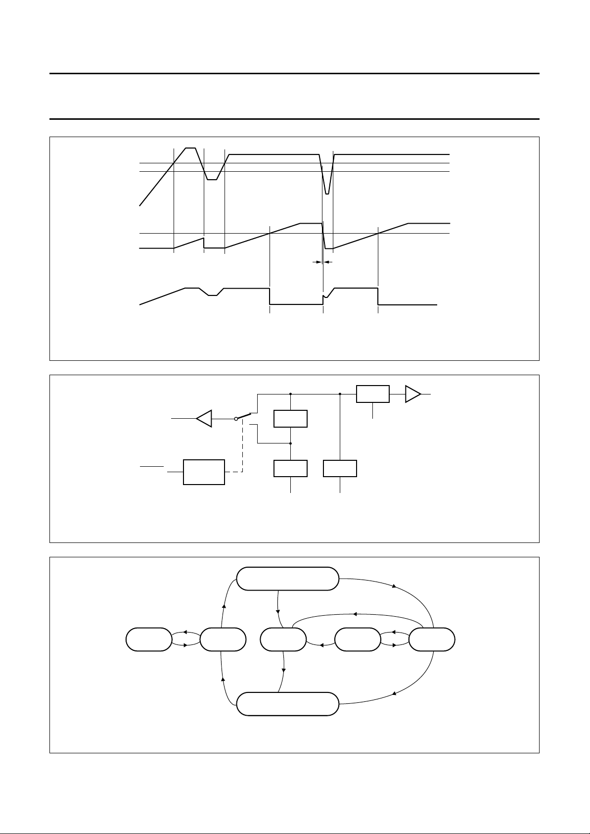
CTIVATION SEQUENCE
A
From the IDLE mode, the circuit enters the ACTIVATION
mode when the microcontroller sets the START line
(active LOW). The I/O(µC) signals must not be LOW.
The internal circuitry is activated, the internal clock starts
and the following ISO 7816 sequence is performed:
1. VCC rises from 0 to 5 V
2. I/Os are enabled
3. VPP rises from 0 to 5 V
4. No change
5. CLK is enabled
6. RST is enabled.
The typical time interval between two steps is 32 µs for the
first two steps and 64 µs for the other three. Timing is
derived from the internal clock (see Fig.6).
1996 Dec 12 5
Philips Semiconductors Product specification
Smart card interface TDA8000; TDA8000T
Between steps 3 and 5, a HIGH level on pin RSTIN allows
the CLK signal to be applied to the card. This feature
facilitates a precise count of CLK periods while waiting for
the card to respond to a reset.
After step 5, RSTIN has no further action on CLK.
After step 6, RST is set to the complementary value of
RSTIN.
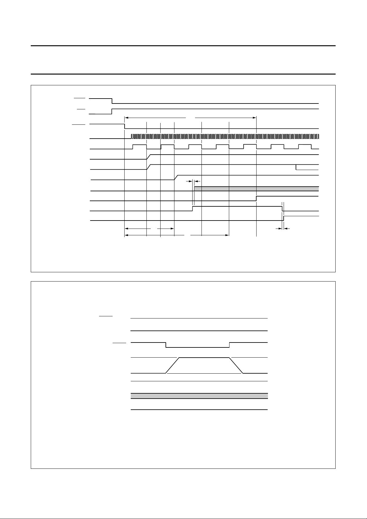
EAD MODE
R
When the activation sequence is completed and, after the
card has replied to its Answer-to-Reset, theTDA8000
enters the READ mode. Data is exchanged between the
card and the microcontroller via the I/O lines.
When it is required to write to the internal memory of the
card, the circuit is set to the WRITE mode by the
microcontroller.
Cards with EPROM memory require a programming
voltage (V
GENERATION
V
PP
PP
).
The circuit supports cards with VPP of 12.5, 15 or 21 V.
The selection of P is achieved by PSEL1 and PSEL2
according to Table 1.
DEACTIVATION SEQUENCE (see Fig.8)
When the session is completed, the microcontroller sets
the START line to its HIGH state.
The circuit then executes an automatic deactivation
sequence by counting back the sequencer:
1. Card reset (RST falls to LOW)
2. CLK is stopped
3. No change
4. VPP falls to 0 V
5. I/O1(µC) and I/O2(µC) become high impedance
6. V
falls to 0 V.
CC
The circuit returns to the IDLE mode on the next rising
edge of the sequencer clock.
P
ROTECTIONS
Main fault conditions are monitored by the circuit:
• Short-circuit on V
• Short-circuit on V
CC
PP
• Over current on I/Os
• Card extraction during transaction
• Overheating problem.
Table 1 Card programming voltage selection
PSEL1 PSEL2
PROGRAMMING
VOLTAGE P
LOW LOW 5
LOW HIGH 12.5
HIGH LOW 15
HIGH HIGH 21
In order to respect the ISO7816 slopes, the circuit
generates V
by charging and discharging an internal
PP
capacitor. The voltage on this capacitor is then amplified
by a power stage gain of 5, powered via an external supply
[30 V (max.)].
pin V
H
RITE MODE (see Fig.7)
W
When the microcontroller sets the WRITE line (active
LOW), the circuit enters the WRITE mode. VPP rises from
5 V to the selected value with a typical slew rate of 1 V/µs.
When the write operation is completed, the microcontroller
returns the WRITE line to its HIGH state, and VPP falls
back to 5 V with the same slew rate.
When one of these fault conditions is detected, the circuit
pulls the interrupt line OFF to its active LOW state and
returns to the FAULT mode.
AULT MODE (see Fig.9)
F
When a fault condition is written to the microcontroller via
the OFF line, the circuit initiates a deactivation sequence.
After the deactivation sequence has been completed, the
OFF line is reset to its HIGH state when the microcontroller
has reset the START line HIGH, except if the fault
condition was due to a card extraction.
Note
The two other causes of emergency deactivation (Power
failure detected on V
DD
or V
) do not act upon OFF.
SUP
WRITE has no action outside a session.
1996 Dec 12 6
Philips Semiconductors Product specification
Smart card interface TDA8000; TDA8000T
handbook, full pagewidth
V
V
DELAY
ALARM
handbook, full pagewidth
SUP
Fig.3 ALARM and DELAY as a function of V
CLKOUT
÷ 2
V
+ V
th2
hys2
V
th2
V
th3
t
d
MGG818
(C
SUP
fixes the pulse width).
DEL
ENABLE
ENCLK
CLK
handbook, full pagewidth
CLKDIV
INPUT
IDLE
OSC INPUT
XTAL CLKIN
Fig.4 Clock circuitry.
ACTIVATION
FAULT READWRITEPDOWN
DEACTIVATION
Fig.5 State diagram.
MGG819
MGG820
1996 Dec 12 7
Philips Semiconductors Product specification
Smart card interface TDA8000; TDA8000T
handbook, full pagewidth
INTERNAL CLOCK
SEQUENCER CLOCK
ENABLE RESET
PRES
OFF
START
V
CC
I/O
V
PP
CLK
RSTIN
RST
INTERNAL
t
act
t
d(clk)
t
3
123 4 5 6
t
5
Fig.6 Activation sequence.
t
RST
MGG821
handbook, full pagewidth
START (LOW)
VCC (+5 V)
WRITE
(P)
(+5 V)
VPP (0 V)
CLK
RST (HIGH)
Fig.7 Read/Write; Read mode.
1996 Dec 12 8
MGG822
 Loading...