

Philips tda7396 DATASHEETS

®
45W/2Ω BRIDGE CAR RADIO AMPLIFIER
HIGH POWER CAPABIL ITY:
- 65W/2Ω MAX
- 60W/2Ω EIAJ
- 45W/2Ω @ V
DIFFERENTIAL INPUTS (EITHER SINGLE
ENDED OR DI FFERENTIAL INPU T SIGNALS
ARE ACC EPTED)
MINIMUM EXTERNAL COMPONENT COUNT:
- NO BOOTSTRAP CAPACITORS
- NO BOUCHEROT CELLS
- INTERNALLY FIXED GAIN (26dB)
- NO SVR CAPACITOR
ST.-BY FUNCTION (CMOS COMPA TIBLE)
AUTOMATIC MUTE DURING TURN-ON /OFF
AUTOMU T E AT MINIM UM SUPPLY
VOLTAGE DETECTION
SYNCHRONIZING PIN FOR SIMULTANEOUS
TURN-ON IN MULTI-DEVICE APPLICATIONS
NO AUDIBLE POP DURING MUTE AND ST-
BY OPERATIONS
Diagnostic Facilities:
CLIPPING DETECTOR
Figure 1: Test And Application Circuit
S
= 14.4V, f = 1KHz, d = 10%
TDA7396
WITH DIAGNOSTIC FACILITY
Multiwatt11
ORDERING NUMBER:
SHORT CIRCUIT
OPEN LOAD
THERMAL SHUTDOWN
PROTECTIONS:
SHORT CIRCUIT ( TO GND, TO VS, ACROSS
THE LOAD)
VERY INDUCTIVE LOADS
CHIP OVER-TEMPERATURE
LOAD DUMP
OPEN GND
ESD
TDA7396
+V
S
7
5
4
GND
100nF
OUT+
OUT-
CD-DIA
0.22µF
IN+
0.22µF
IN-
STANDBY
TO µC or V
April 2002
This is advanced information on a new product now in development or undergoing evaluation. Details are subject to change without notice.
S
CM
10µF
D93AU004
39
2
1
TDA7396
8
11
10 6
RS
51KΩ
1000µF
Vref
10KΩ
TO µC
1/11
TDA7396
DESCRIPTION
The TDA7396 is a BRIDGE class AB audio power
amplifier especially intended for car radio High
Power applications.
The 2Ω power capability together with the possibility to operate eit her in DIFFERENTIAL INPUT
MODE or SINGLE ENDED INPUT MODE makes
it suitable for boosters and high end car r adio ap-
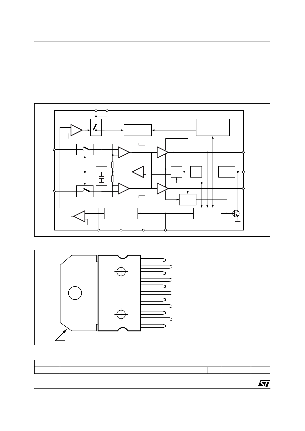
Figure 2: Block Diagram
V
CC1VCC2
39
IN-
IN+
+
-
ST ANDBY THRESHOLD
1
ICM
2
500Ω
500Ω
-
+
gm
REFERENCES
10K
COMMON
MODE
-
+
V
CC/2
10K
plications.
The exclusive fully complementary output stage
and the internally fixed gain configuration drop the
external component count.
The on board clipping detector allows easy implementation of gain compression systems.
The diagnostics facility allows to detect any mistakes during car radio set assembly and wiring in
the car.
SHORT CIRCUIT
DUMP & THERMAL
PROTECTION
5
POWER AMP
LTS
POWER AMP
DETECT
THD
V=f
(Tj)
LTS
DISABLE
OUT-
4
DIAGN
CD
7
OUT+
+
-
MUTE THRESHOLD
MUTE SYNC GND STANDBY
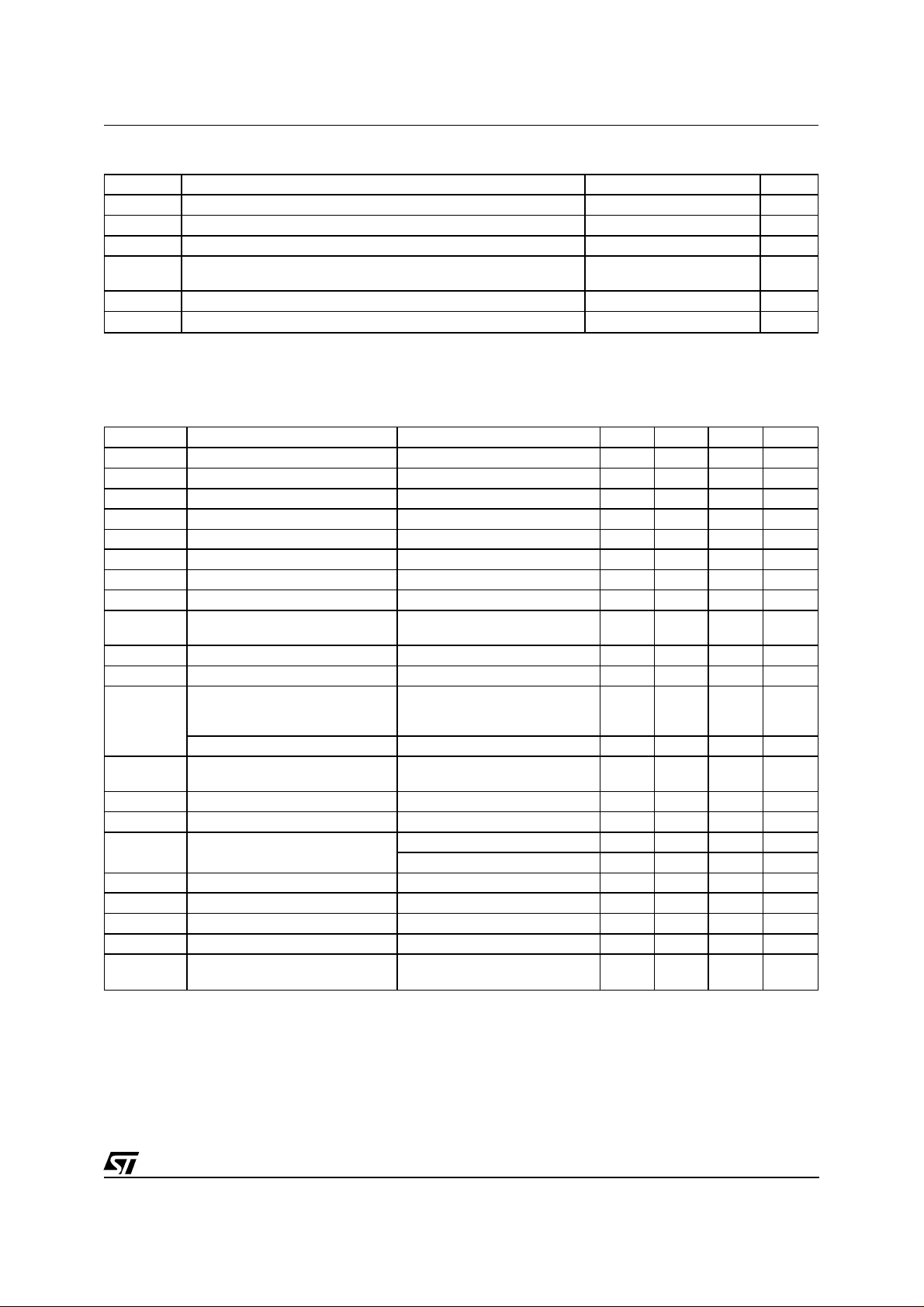
PIN CONNECTION (Top view)
TAB CONNECTED TO PIN 6
THERMAL DATA
PROGRAMMABLE
CURRENT CIRCUIT
1011 8
11
10
DIAGNOSTIC
CIRCUIT
6
D94AU107
MUTE
SYNC
9
8
7
6
5
4
3
2
1
D93AU003A
+V
S
STAND-BY
OUT+
GND
OUT-
CD-DIA (CLIPPING DETECTOR - DIAG.)
+V
S
IN+
IN-
Symbol Description Value Unit
R
th j-case
Thermal Resistance Junction-case Max 1.5
2/11
C/W
°
TDA7396
ABSOLUTE MAXIMUM RATINGS
Symbol Parameter Value Unit
DC Supply Voltage 28 V
S
Operating Supply Voltage 18 V
Peak Supply Voltage (t = 50ms) 50 V
Output Peak Current repetitive (f > 10Hz)
Output Peak Current non repetitive
Power Dissipation (T
= 85°C) 43 W
CASE
6
7
, TjStorage and Junction-Case -40 to 150
A
A
C
°
T
V
V
V
OP
PEAK
I
P
stg
O
tot
ELECTRICAL CHARACTERISTICS (V
= 14.4V; RL = 2Ω, f = 1KHz, T
S
= 25°C, unless otherwise
amb
specified)
Symbol Parameter Test Condition Min. Typ. Max. Unit
V
S
I
q
V
OS
I
SB
I
SBin
V
SBon
V
SBoff
ATT
ST-BY
R
EXT/RS
I
M in
A
M
P
O
d Distortion PO = 0.1 to 20W
G
V
f
H
R
IN
E
IN
CMRR Input Common Mode Rejection f = 1KHz; V
SVR Supply Voltage Rejection Rg = 0Ω; Vr = 1Vrms 60 dB
CDL Clipping Detection Level 0.5 %
T
sd
Supply Voltage Range 8 18 V
Total Quiescent Current 100 mA
Output Offset Voltage 150 mV
ST-BY Current V
ST-BY Input Bias Current V
= 1.5V 100
ST-BY
= 5V 10
ST-BY
ST-BY On Threshold Voltage 1.5 V
ST-BY Off threshold Voltage 3.5 V
ST-BY Attenuation 90 dB
Mute Resistor Ratio for External
(see Application Circuit of fig. 4) 0.63 0.69 V
Mute Control
Mute Input Bias Current V
= 5V 10
MUTE
Mute Attenuation 90 dB
RMS Output Power d = 10%
d = 1%
d = 10%; R
EIAJ Output Power V
= 13.7V 60 W
S
L
= 4
Ω
45
35
27
0.06
= 0.1 to 15W; RL = 4
P
O
Ω
0.03
Voltage Gain 25 26 27 dB
High Frequency rolloff PO = 1W; -3dB 75 KHz
Input Impedance Differential 60 K
Single Ended 55 K
Input Noise Voltage Rg = 0Ω ; f = 22Hz to 22KHz 4
= 1Vrms 70 dB
IN
Absolute Thermal Shutdown
160 dB
Junction Temperature
A
µ
A
µ
A
µ
W
W
W
%
%
Ω
Ω
V
µ
3/11

TDA7396
FUNCTIONAL DESCRIPTION
Pin Function Description
1, 2 INPUTS
4 CD - DIA
5, 7 OUTPUTS
8 STAND-BY
10 SYNC
11 MUTE
The input stage is a high impedance differential type also capable of operation in single
ended mode with one input capacitively coupled to the signal GND. the impedance seen
by the inverting and non inverting input pins must be matched.
The TDA7396 is equipped with a diagnostics circuitry able to detect the following events:
- Clipping in the Output Signal
- Thermal Shutdown
- Open Load (before turn-on)
- Shorted Output: to GND, to Vs, across the load (after turn-on)
The CD-DIA(open collector) pin gives out the diagnostics signal (low during clipping or
output fault condition).
The device does not work as long as the faulty condition holds; the normal operation is
automatically restored after the fault removal.
The output stage is a bridge type able to drive loads as high as 2Ω.
It consists of two class AB fully complementary PNP/NPN stages fully protected.
A rail to rail output voltage swing is achieved with no need of bootstrap capacitors.
No external compensation is necessary.
The device features a ST-BY function which shuts down all the internal bias supplies
when the ST-BY input is low.
In ST-BY mode the amplifier sinks a small current (in the range of few µA).
When the ST-BY pin is high the IC becomes fully operational.
A resistor (R
current that flows into C
required to bias the amplifier.
a) The pin will have a capacitor (C
automatic Mute during turn on/off is provided to prevent noisy transients
b) If a independent Mute function is needed, an external transistor circuit (see fig. 4) may
be connected to this pin; 1% precision resistors have to be used for R
to reach the fixed limits 0.63 ≤ R
) has to be connect between pin 10 and GND in order to program the
S
capacitor (pin 11). The values of CM and RS determine the time
M
) tied to GND to set the MUTE/STAND-BY time. An
M
/ R
0.69
EXT
≤
S
/ RS in to order
EXT
Figure 3: Application Circuit with External Mute Control
0.22µF
IN+
39
2
0.22µF
IN-
1
TDA7396
TO µC
STANDBY
TO µC or V
S
REXT
8
11
10 6
CM
RS
7
5
4
GND
100nF
OUT+
OUT-
CD-DIA
1000µF
Vref
10KΩ
D93AU007
+V
S
TO µC
4/11
 Loading...