

Philips tda7313 DATASHEETS
DIGITAL CONTROLLED STEREO AUDIO PROCESSOR
INPUTMULTIPLEXER:
- 3 STEREOINPUTS
- SELECTABLEINPUT GAINFOROPTIMAL
ADAPTIONTO DIFFERENTSOURCES
INPUT AND OUTPUT FOR EXTERNAL
EQUALIZER OR NOISE REDUCTION SYSTEM
LOUDNESSFUNCTION
VOLUMECONTROLIN 1.25dBSTEPS
TREBLEAND BASSCONTROL
FOURSPEAKERATTENUATORS:
- 4 INDEPENDENTSPEAKERSCONTROL
IN 1.25dB STEPS FOR BALANCEAND
FADERFACILITIES
- INDEPENDENT MUTEFUNCTION
ALL FUNCTIONS PROGRAMMABLE VIA SE-
2
RIAL I
DESCRIPTION
The TDA7313 is a volu me, tone (bass and treble)
balance (Left/Right) and fader (front/rear) processor
for quality audio applications in car radio and Hi-Fi
C BUS
TDA7313
WITH LOUDNESS
ADVANCE DATA
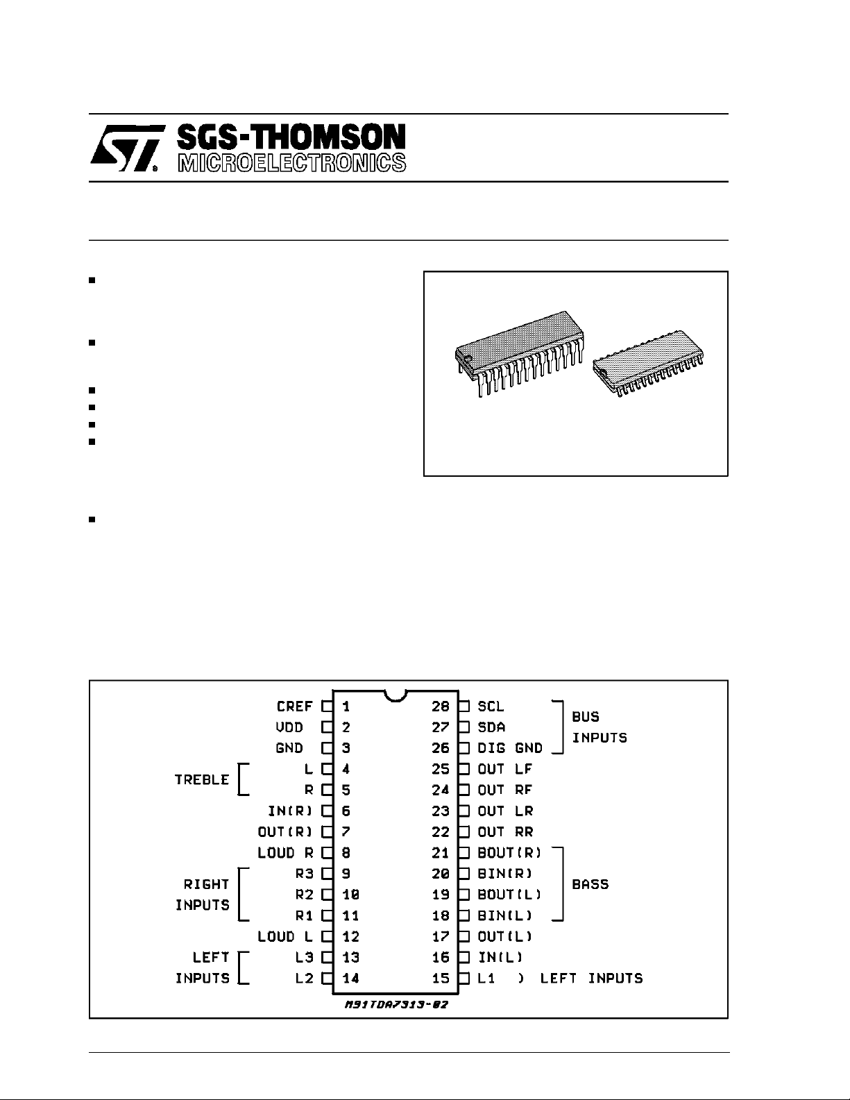
DIP28 SO28
ORDERING NUMBERS:
TDA7313 TDA7313D
systems.
Selec ta bl einput gainand externalloudnessfunction
are provided. Cont r ol is accompli shed by serial I
bus microprocessorinterfac e.
TheAC signalsettingisobtainedbyres i s t ornetworks
andswitchescombinedwith operatio nalam pl ifi er s .
Thanks to the used BIPOLAR/CMO S Tecnology,
Low Distortion,LowNoiseandLow DC steppingare
obtained.
2
C
PIN CONNECTION (Top view)
February 1994
This is advanced informationon a new productnow in development or undergoing evaluation. Details are subject to change without notice.
1/14
TDA7313
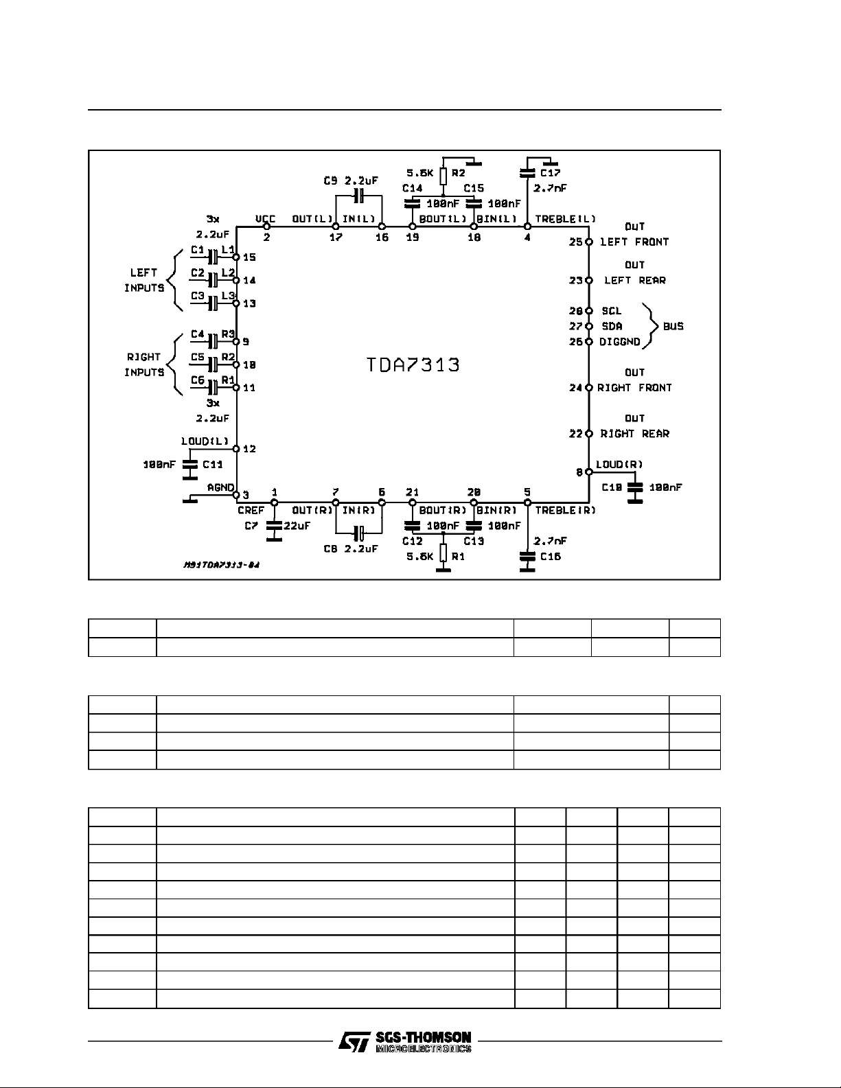
TEST CIRCUIT
THERMAL DATA
Symbol Description SO28 DIP28 Unit
R
th j-pins
Thermal Resistance Junction-pins max 85 65 °C/W
ABSOLUTE MAXIMUMRATINGS
Symbol Parameter Value Unit
V
T
amb
T
stg
Operating Supply Voltage 10.2 V
S
Operating Ambient Temperature -40 to 85 °C
Storage Temperature Range -55 to +150 °C
QUICK REFERENCE DATA
Symbol Parameter Min. Typ. Max. Unit
V
V
CL
THD Total Harmonic Distortion V = 1Vrms f = 1KHz 0.01 0.1 %
S/N Signal to NoiseRatio 106 dB
S
Supply Voltage 6 9 10 V
S
Max. inputsignal handling 2 Vrms
Channel Separation f = 1KHz 103 dB
C
Volume Control 1.25dB step -78.75 0 dB
Bass and Treble Control 2db step -14 +14 dB
Fader and BalanceControl 1.25dB step -38.75 0 dB
Input Gain 3.75dB step 0 11.25 dB
Mute Attenuation 100 dB
2/14
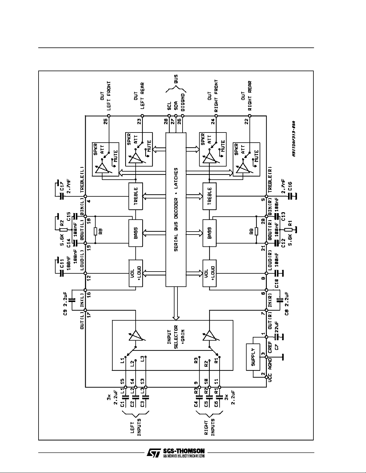
BLOCK DIAGRAM
TDA7313
3/14
TDA7313
ELECTRICALCHARACTERISTICS (referto the test circuitT
= 600Ω, all controls flat (G = 0), f =1KHz unless otherwise specified)
R
G
=25°C,VS=9V, RL= 10KΩ,
amb
Symbol Parameter Test Condition Min. Typ. Max. Unit
SUPPLY
V
S
I
S
SVR Ripple Rejection 60 80 dB
Supply Voltage 6 9 10 V
Supply Current 8 11 mA
INPUTSELECTORS
G
G
G
V
R
II
V
CL
S
IN
R
L
INmin
INmax
STEP
e
IN
DC
Input Resistance Input 1, 2, 3 35 50 70 KΩ
ClippingLevel 2 2.5 Vrms
Input Separation (2) 80 100 dB
Output Load resistance pin 7, 17 2 KΩ
Min. Input Gain -1 0 1 dB
Max. Input Gain 11.25 dB
Step Resolution 3.75 dB
Input Noise G = 11.25dB 2 µV
DC Steps adjacent gain steps 4 20 mV
G = 18.75 to Mute 4 mV
VOLUMECONTROL
R
IV
C
RANGE
A
VMIN
A
VMAX
A
STEP
E
A
E
T
V
DC
Input Resistance 20 33 50 kΩ
Control Range 70 75 80 dB
Min. Attenuation -1 0 1 dB
Max. Attenuation 70 75 80 dB
Step Resolution 0.5 1.25 1.75 dB
Attenuation Set Error Av = 0 to -20dB
Av =-20 to -60dB
-1.25
-3
0 1.25
2
Tracking Error 2dB
DC Steps adjacent attenuation steps
From 0dB to Av max
0
0.5
3
7.5
SPEAKERATTENUATORS
dB
dB
mV
mV
C
S
A
range
STEP
E
MUTE
V
DC
A
Control Range 35 37.5 40 dB
Step Resolution 0.5 1.25 1.75 dB
Attenuation set error 1.5 dB
Output Mute Attenuation 80 100 dB
DC Steps adjacent att. steps
from 0to mute
0
1
BASSCONTROL (1)
Gb Control Range Max. Boost/cut +12 +14 +16 dB
B
STEP
R
B
Step Resolution 1 2 3 dB
Internal Feedback Resistance 34 44 58 KΩ
TREBLECONTROL (1)
Gt Control Range Max. Boost/cut +13 +14 +15 dB
Step Resolution 1 2 3 dB
4/14
T
STEP
10
3
mV
mV
TDA7313
ELECTRICALCHARACTERISTICS (continued)
Symbol Parameter Test Condition Min. Typ. Max. Unit
AUDIOOUTPUTS
V
OCL
R
L
C
L
R
OUT
V
OUT
ClippingLevel d = 0.3% 2 2.5 Vrms
Output Load Resistance 2 KΩ
Output Load Capacitance 10 nF
Output resistance 30 75 120 Ω
DC Voltage Level 4.2 4.5 4.8 V
GENERAL
e
NO
S/N Signal to Noise Ratio all gains= 0dB; V
d Distortion A
Sc Channel Separation left/right 80 103 dB
Output Noise BW = 20-20KHz, flat
output muted
all gains= 0dB
A curve all gains = 0dB 3 µV
O
=0,VIN= 1Vrms
V
A
= -20dB VIN= 1Vrms
Total Tracking error A
V
= 0to -20dB
V
V
= 0.3Vrms
IN
-20 to -60 dB
2.5
515
µV
µV
= 1Vrms 106 dB
0.01
0.09
0.04
0
0
0.1
0.3
1
2
%
%
%
dB
dB
BUS INPUTS
V
IL
V
IH
I
IN
V
O
Notes:
(1) Bassand Treble response see attached diagram (fig.16). The center frequency andquality of the resonance behaviour can be choosen by
the external circuitry. A standard first order bassresponse can be realized by a standard feedbacknetwork
(2) The selected input is grounded thru the 2.2µF capacitor.
Input Low Voltage 1V
Input High Voltage 3 V
Input Current -5 +5 µA
Output Voltage SDA
IO= 1.6mA 0.4 V
Acknowledge
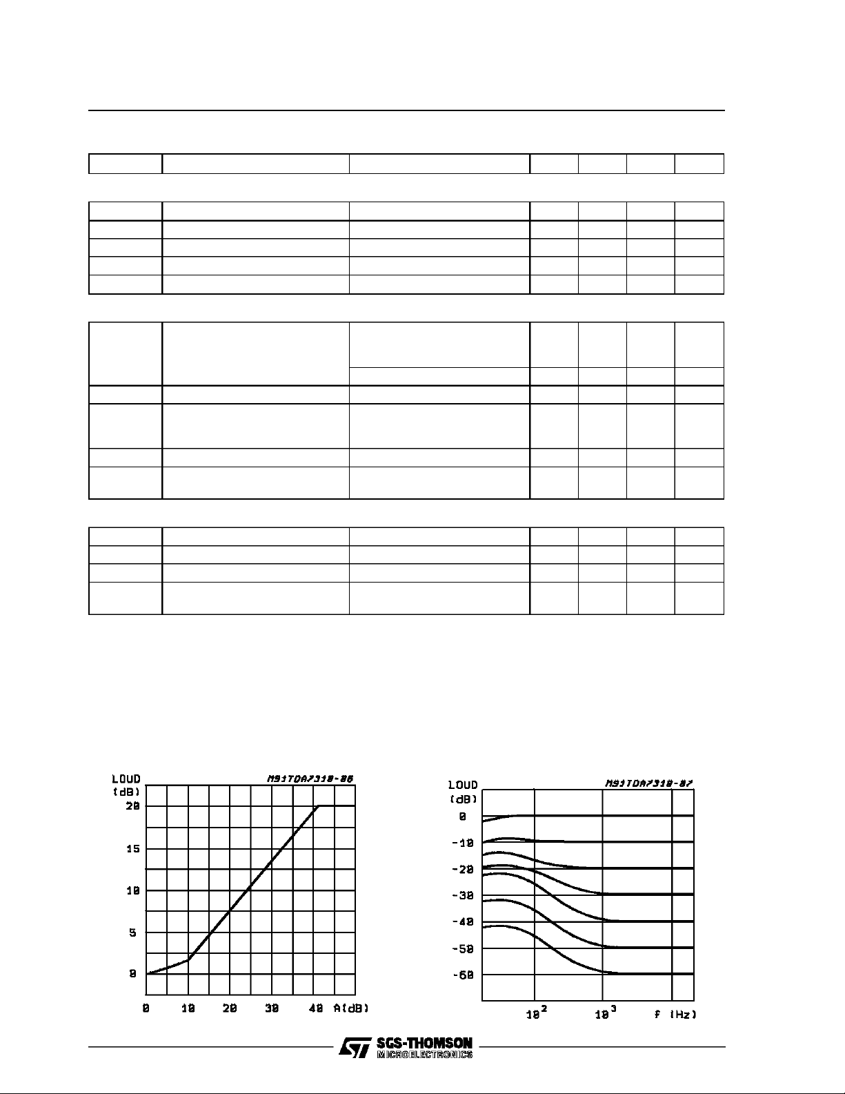
Figure1: Loudnessvs. VolumeAttenuation
Figure2: Loudness vs. Frequency(C
100nF) vs. Volume Attenuation
LOUD
=
5/14
 Loading...