

Philips tda7294 DATASHEETS

®
TDA7294
100V - 100W DMOS AUDIO AMPLIFIER WITH MUTE/ST-BY
VERY HIG H OPERATI NG VOLTAGE R ANGE
(±40V)
DMOS POWER STAGE
HIGH OUTPUT POWER (UP TO 100W MU-
SIC POWER)
MUTING/STAND- BY FUNC TION S
NO SWITCH ON/OFF NOISE
NO BOUCHEROT CELLS
VERY LOW DISTORTION
VERY LOW NOISE
SHORT CIRCUIT PROTECTION
THERMAL SHUTDOWN
DESCRIPTION
The TDA7294 is a monolithic integrated circuit in
Multiwatt15 package, intended for use as audio
class AB amplifier in Hi-Fi field applications
(Home Stereo, self powered loudspeakers, Topclass TV). Thanks to the wide voltage range and
Figure 1: Typical Application and Test Circuit
MULTIPOWER BCD TECHNOLOGY
Multiwatt15V Multiwatt15H
ORDERING NUMBERS:
TDA7294V TDA7294HS
to the high out current c apability it is able to supply the highest power into both 4Ω and 8Ω loads
even in presence of poor supply regulation, with
high Supply Voltage Rejection.
The built in muting function with turn on delay
simplifies the remote operation avoiding switching
on-off noises.
+VsC7 100nF C6 1000µF
VM
VSTBY
January 2003
C2
R2
22µF
680Ω
C1 470nF
R1 22K
R5 10K
R4 22K
C3 10µF C4 10µF
IN- 2
IN+
IN+MUTE
MUTE
STBY
R3 22K
3
4
10
9
TDA7294
MUTE
STBY
1
STBY-GND
+PWVs+Vs
713
-
+
THERMAL
SHUTDOWN
-Vs -PWVs
C9 100nF C8 1000µF
-Vs
S/C
PROTECTION
158
14
6
OUT
C5
22µF
BOOTSTRAP
D93AU011
1/17
TDA7294
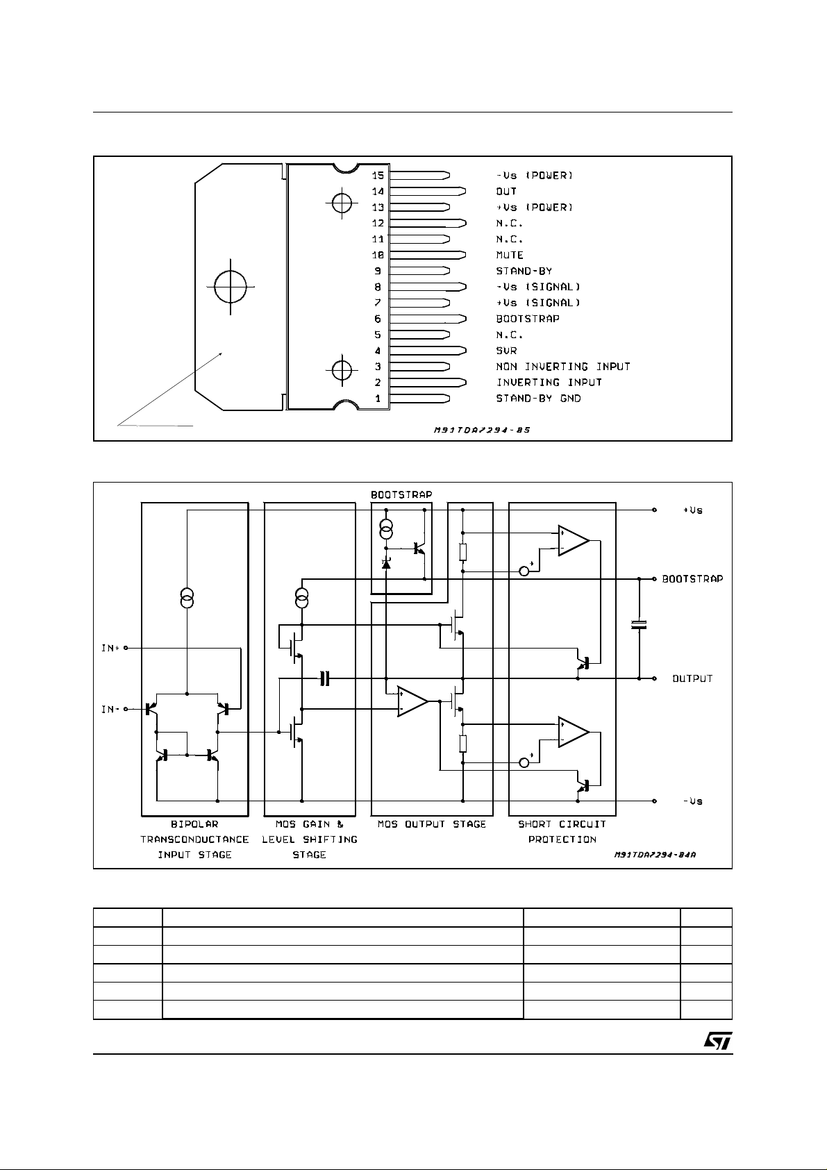
PIN CONNECTION (Top view)
TAB connected to -V
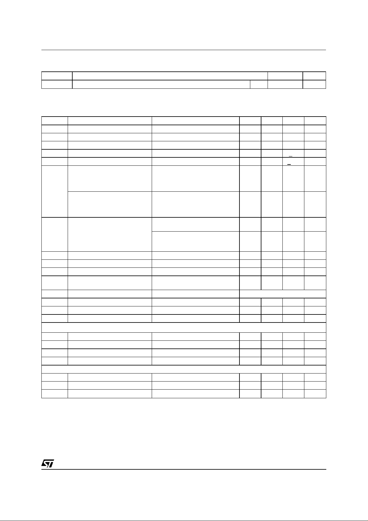
BLOCK DIAGRAM
S
ABSOLUTE MAXIMUM RATINGS
Symbol Parameter Value Unit
V
I
O
P
tot
T
op
T
stg
Supply Voltage (No Signal)
S
Output Peak Current 10 A
Power Dissipation T
= 70°C50W
case
Operating Ambient Temperature Range 0 to 70
, TjStorage and Junction Temperature 150
2/17
50 V
±
C
°
C
°
TDA7294
THERMAL DATA
Symbol Description Value Unit
R
th j-case
Thermal Resistance Junction-case Max 1.5
C/W
°
ELECTRICAL CHARACTERISTICS (Refer to the Test Circuit V
= 50 Ω; T
R
g
= 25°C, f = 1 kHz; unless otherwise specified.
amb
= ±35V, RL = 8Ω, GV = 30dB;
S
Symbol Parameter Test Condition Min. Typ. Max. Unit
V
I
I
V
I
OS
P
Supply Range
S
Quiescent Current 20 30 65 mA
q
Input Bias Current 500 nA
b
Input Offset Voltage +10 mV
OS
Input Offset Current +100 nA
RMS Continuous Output Power d = 0.5%:
O
Music Power (RMS)
IEC268.3 RULES - ∆t = 1s (*)
d Total Harmonic Distortion (**) P
V
= ± 35V, RL = 8
S
V
= ± 31V, RL = 6
S
V
= ± 27V, RL = 4
S
Ω
Ω
Ω
d = 10%
R
= 8Ω ; VS = ±38V
L
R
= 6Ω ; VS = ±33V
L
R
= 4Ω ; VS = ±29V (***)
L
= 5W; f = 1kHz
O
P
= 0.1 to 50W; f = 20Hz to 20kHz
O
= ±27V, RL = 4
V
S
P
= 5W; f = 1kHz
O
P
= 0.1 to 50W; f = 20Hz to 20kHz
O
Ω:
10
±
60
60
60
70
70
70
100
100
100
0.005
0.01
40 V
±
0.1
0.1
W
W
W
W
W
W
%
%
%
%
SR Slew Rate 7 10 V/µs
G
G
e
, f
f
L
R
SVR Supply Voltage Rejection f = 100Hz; V
T
STAND-BY FUNCTION (Ref: -V
V
ST on
V
ST off
ATT
I
q st-by
MUTE FUNCTION (Ref: -V
V
Mon
V
Moff
ATT
Note (*):
MUSIC POWER CONCEPT
MUSIC POWER is the maximal power which the amplifier is capable of producing across the rated load resistance (regardless of non linearity)
1 sec after the application of a sinusoidal input signal of frequency 1KHz .
Note (**):
Note (***):
Open Loop Voltage Gain 80 dB
V
Closed Loop Voltage Gain 24 30 40 dB
V
Total Input Noise A = curve
N
f = 20Hz to 20kHz
Frequency Response (-3dB) PO = 1W 20Hz to 20kHz
H
Input Resistance 100 k
i
= 0.5Vrms 60 75 dB
ripple
Thermal Shutdown 145
S
or GND)
S
1
25
Stand-by on Threshold 1.5 V
Stand-by off Threshold 3.5 V
Stand-by Attenuation 70 90 dB
st-by
Quiescent Current @ Stand-by 1 3 mA
or GND)
S
Mute on Threshold 1.5 V
Mute off Threshold 3.5 V
Mute AttenuatIon 60 80 dB
mute
Tested with optimized Application Board (see fig. 2)
Limited by the max. allowable current.
V
µ
V
µ
Ω
C
°
3/17
TDA7294
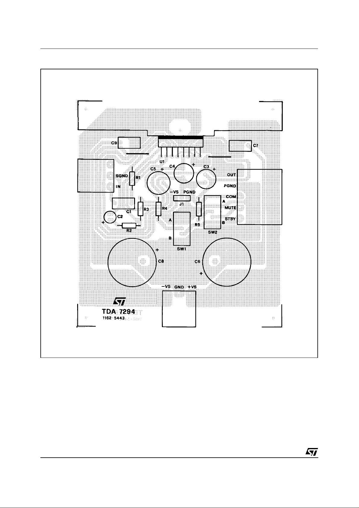
Figure 2: P.C.B. and components layout of the circuit of figure 1. (1:1 scale)
Note:
The Stand-by and Mute functions can be referred either to GND or -VS.
On the P.C.B. is possible to set both the configuration through the jumper J1.
4/17
TDA7294
APPLICATION SUGGES TION S (see Test and Application Circuits of the Fig. 1)
The recommended values of t he external components are t hose shown on t he application circuit o f Figure 1. Different values can be used; the following table can help the designer.
COMPONENTS SUGGESTED VALUE PURPOSE
R1 (*) 22k INPUT RESISTANCE INCREASE INPUT
R2 680
R3 (*) 22k INCREASE OF GAIN DECREASE OF GAIN
R4 22k ST-BY TIME
R5 10k MUTE TIME
C1 0.47µF INPUT DC
C2 22µF FEEDBACK DC
C3 10µF MUTE TIME
C4 10µF ST-BY TIME
Ω
CLOSED LOOP GAIN
SET TO 30dB (**)
CONSTANT
CONSTANT
DECOUPLING
DECOUPLING
CONSTANT
CONSTANT
LARGER THAN
SUGGESTED
IMPRDANCE
DECREASE OF GAIN INCREASE OF GAIN
LARGER ST-BY
ON/OFF TIME
LARGER MUTE
ON/OFF TIME
LARGER MUTE
ON/OFF TIME
LARGER ST-BY
ON/OFF TIME
SMALLER THAN
SUGGESTED
DECREASE INPUT
IMPEDANCE
SMALLER ST-BY
ON/OFF TIME;
POP NOISE
SMALLER MUTE
ON/OFF TIME
HIGHER LOW
FREQUENCY
CUTOFF
HIGHER LOW
FREQUENCY
CUTOFF
SMALLER MUTE
ON/OFF TIME
SMALLER ST-BY
ON/OFF TIME;
POP NOISE
C5 22µF BOOTSTRAPPING SIGNAL
C6, C8 1000µF SUPPLY VOLTAGE
C7, C9 0.1µF SUPPLY VOLTAGE
(*) R1 = R3 FOR POP OPTIMIZATION
(**) CLOSED LOOP GAIN HAS TO BE ≥ 24dB
BYPASS
BYPASS
DEGRADATION AT
LOW FREQUENCY
DANGER OF
OSCILLATION
DANGER OF
OSCILLATION
5/17
TDA7294
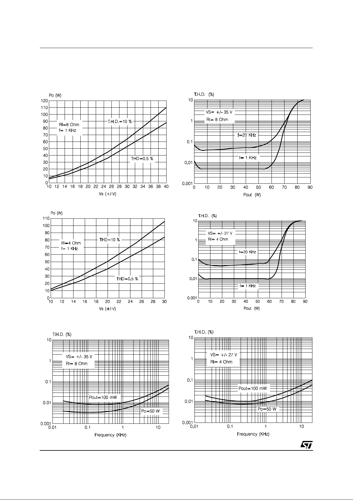
TYPICAL CHARACTERISTICS
(Application Circuit of fig 1 unless otherwise specified)
Figure 3: Output Power vs. Supply Voltage.
Figure 5: Output Power vs. Supply Voltage
Figure 4: Distortion vs. Output Power
Figure 6: Distortion vs. Output Power
Figure 7: Distortion vs. Frequency
6/17
Figure 8: Distortion vs. Frequency
 Loading...