

Philips tda7073a, tda7073 at DATASHEETS

INTEGRATED CIRCUITS
DATA SH EET
TDA7073A; TDA7073AT
Dual BTL power driver
Product specification
Supersedes data of 1994 July
File under Integrated Circuits, IC01
1999 Aug 30
Philips Semiconductors Product specification
Dual BTL power driver TDA7073A; TDA7073AT
FEATURES
• No external components
• Very high slew rate
• Single power supply
• Short-circuit proof
GENERAL DESCRIPTION
The TDA7073A/AT aredual power driver circuits in a BTL
configuration, intended for use as a power driver for servo
systems with a single supply. They are specially designed
for compact disc players and are capable of driving focus,
tracking, sled functions and spindle motors.
• High output current (0.6 A)
• Wide supply voltage range
• Low output offset voltage
• Suited for handling PWM signals up to 176 kHz
• ESD protected on all pins.
Missing Current Limiter (MCL)
A MCL protection circuit is built-in. The MCL circuit is
activated when the difference in current between the
output terminal of each amplifier exceeds 100 mA (typical
300 mA). This level of 100 mA allows for headphone
applications (single-ended).
QUICK REFERENCE DATA
SYMBOL PARAMETER CONDITIONS MIN. TYP. MAX. UNIT
V
P
G
v
I
P
positive supply voltage range 3.0 5.0 18 V
voltage gain 32.5 33.5 34.5 dB
total quiescent current VP=5V; RL=∞−816mA
SR slew rate − 12 − V/µs
I
I
f
O
bias
co
output current −−0.6 A
input bias current − 100 300 nA
cut-off frequency −3dB − 1.5 − MHz
ORDERING INFORMATION
PACKAGE
TYPE NUMBER
NAME DESCRIPTION VERSION
TDA7073A DIP16 plastic dual in-line package; 16 leads (300 mil); long body SOT38-1
TDA7073AT SO16 plastic small outline package; 16 leads; body width 7.5 mm SOT162-1
1999 Aug 30 2
Philips Semiconductors Product specification
Dual BTL power driver TDA7073A; TDA7073AT
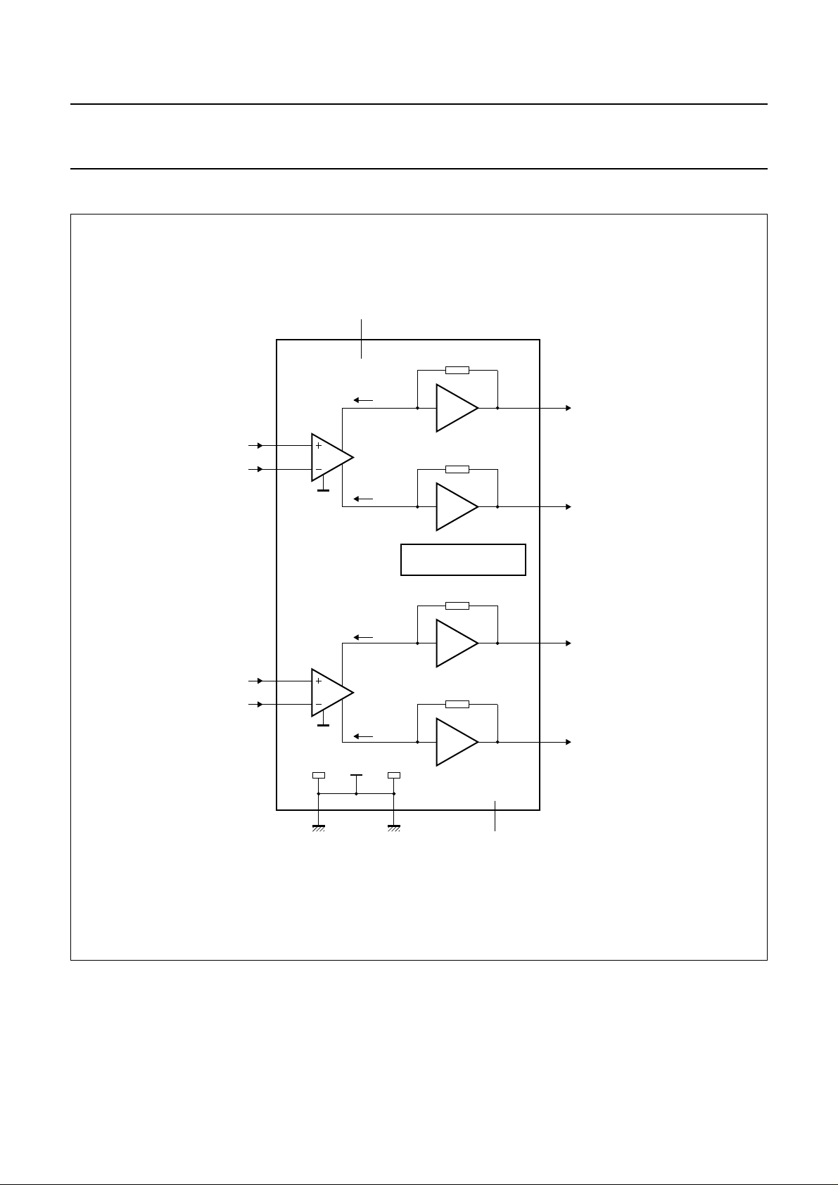
BLOCK DIAGRAM
V
P
handbook, full pagewidth
positive input 1
negative input 1
positive input 2
negative input 2
2
1
TDA7073A
TDA7073AT
6
7
5
Ι
SHORT - CIRCUIT AND
THERMAL PROTECTION
I – i
ΙΙ
16I + i
13I – i
12
9I + i
positive output 1
negative output 1
negative output 2
positive output 2
10
ground 2
14
ground 1
Fig.1 Block diagram.
1999 Aug 30 3
3, 4, 8, 11, 15
MCD382 - 1
n.c.
Philips Semiconductors Product specification
Dual BTL power driver TDA7073A; TDA7073AT
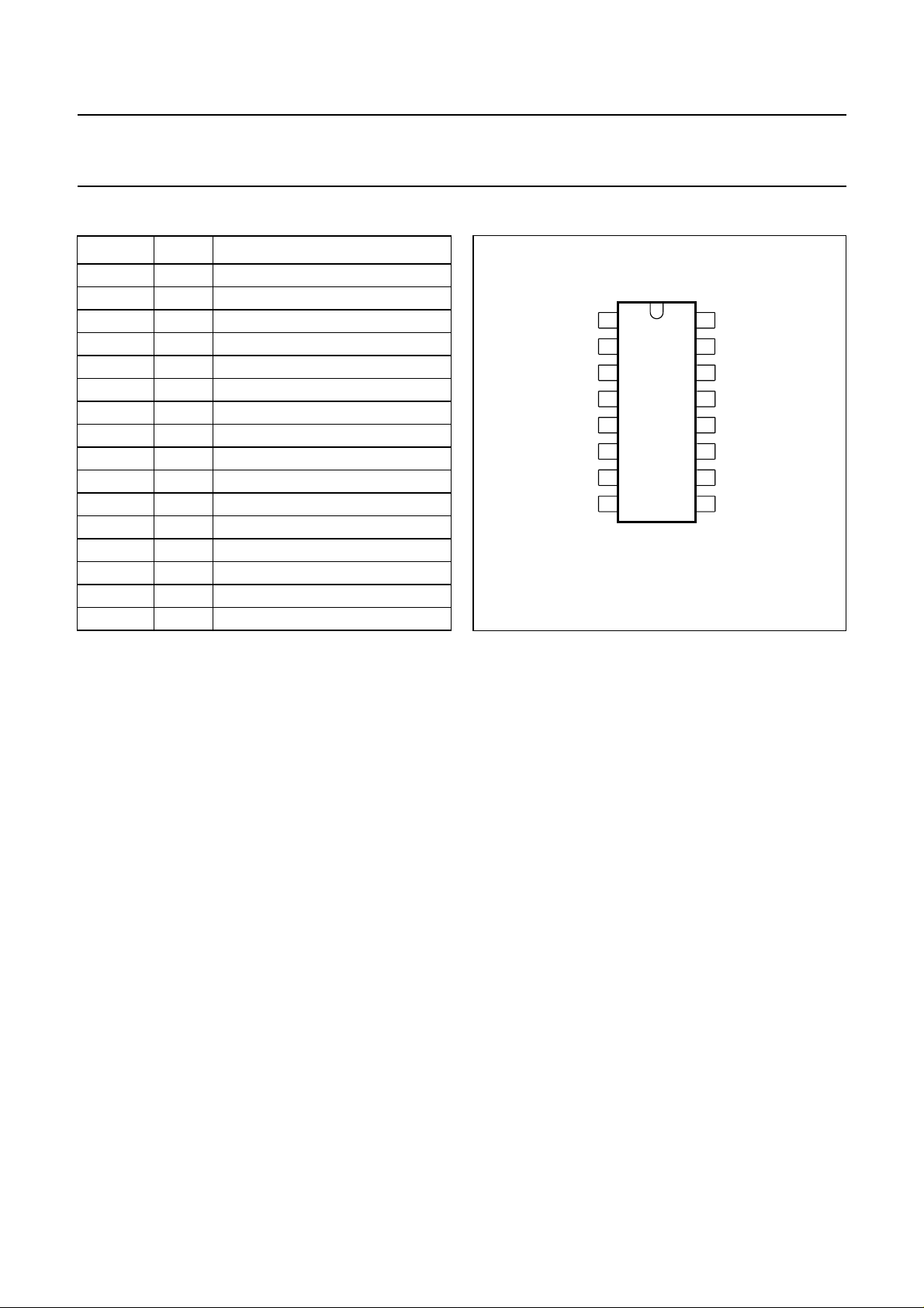
PINNING
SYMBOL PIN DESCRIPTION
IN1− 1 negative input 1
IN1+ 2 positive input 1
n.c. 3 not connected
n.c. 4 not connected
V
P
5 positive supply voltage
IN2+ 6 positive input 2
IN2− 7 negative input 2
n.c. 8 not connected
OUT2+ 9 positive output 2
GND2 10 ground 2
n.c. 11 not connected
OUT2− 12 negative output 2
OUT1− 13 negative output 1
GND1 14 ground 1
n.c. 15 not connected
OUT1+ 16 positive output 1
handbook, halfpage
1
IN1–
IN1+
2
3
n.c.
4
n.c.
V
IN2 +
IN2 –
n.c.
P
TDA7073A
TDA7073AT
5
6
7
8
MCD381
Fig.2 Pin configuration.
16
15
14
13
12
11
10
9
OUT1+
n.c.
GND1
OUT1 –
OUT2 –
n.c.
GND2
OUT2 +
FUNCTIONAL DESCRIPTION
The TDA7073A/AT are dual power driver circuits in a BTL
configuration, intended for use as a power driver for servo
systemswith a single supply. Theyareparticular designed
for compact disc players and are capable of driving focus,
tracking, sled functions and spindle motors.
Because of the BTL configuration, the devices can supply
a bi-directional DC current in the load, with only a single
supply voltage. The voltage gain is fixed by internal
feedback at 33.5 dB and the devices operate in a wide
supply voltage range (3 to 18 V). The devices can supply
a maximum output current of 0.6 A. The outputs can be
short-circuited over the load, to the supply and to ground
at all input conditions. The differential inputs can handle
common mode input voltages from ground level up to
(VP− 2.2 V with a maximum of 10 V). The devices have a
very high slew rate. Due to the large bandwidth, they can
handle PWM signals up to 176 kHz.
1999 Aug 30 4

Philips Semiconductors Product specification
Dual BTL power driver TDA7073A; TDA7073AT
LIMITING VALUES
In accordance with the Absolute Maximum System (IEC 134).
SYMBOL PARAMETER CONDITIONS MIN. MAX. UNIT
V
P
I
ORM
I
OSM
P
tot
T
stg
T
vj
T
sc
Note
1. The outputs can be short-circuited over the load, to the supply and to ground at all input conditions.
positive supply voltage range − 18 V
repetitive peak output current − 1A
non repetitive peak output current − 1.5 A
total power dissipation
TDA7073A T
TDA7073AT T
<25°C − 2.5 W
amb
<25°C − 1.32 W
amb
storage temperature range −55 +150 °C
virtual junction temperature − 150 °C
short-circuit time see note 1 − 1hr
THERMAL CHARACTERISTICS
SYMBOL PARAMETER CONDITIONS VALUE UNIT
R
th (j-a)
from junction to ambient
TDA7073A in free air; note 1 50 K/W
TDA7073AT in free air; note 2 95 K/W
Notes
1. TDA7073A: V
P
=2×0.76 W = 1.52 W; T
tot
= 5 V; RL=8Ω; The typical voltage swing = 5.8 V and V
P
amb (max)
= 150 − 1.52 × 50 = 74 °C.
2. TDA7073AT: VP= 5 V; RL=16Ω; typical voltage swing = 5.8 V and V
P
=2×0.38 W = 0.76 W; T
tot
amb (max)
= 150 − 0.76 × 95 = 77 °C.
is 2.1 V therefore IO= 0.36 A and
loss
is 2.1 V therefore IO= 0.18 A and
loss
1999 Aug 30 5
 Loading...