

Philips tda7053a DATASHEETS
INTEGRATED CIRCUITS
DATA SH EET
TDA7053A
Stereo BTL audio output amplifier
with DC volume control
Objective specification
Supersedes data of May 1995
File under Integrated Circuits, IC01
1995 Nov 09
Philips Semiconductors Objective specification
Stereo BTL audio output amplifier with
TDA7053A
DC volume control
FEATURES
• DC volume control
• Few external components
• Mute mode
• Thermal protection
• Short-circuit proof
• No switch-on and switch-off clicks
• Good overall stability
• Low power consumption
• Low HF radiation
• ESD protected on all pins.
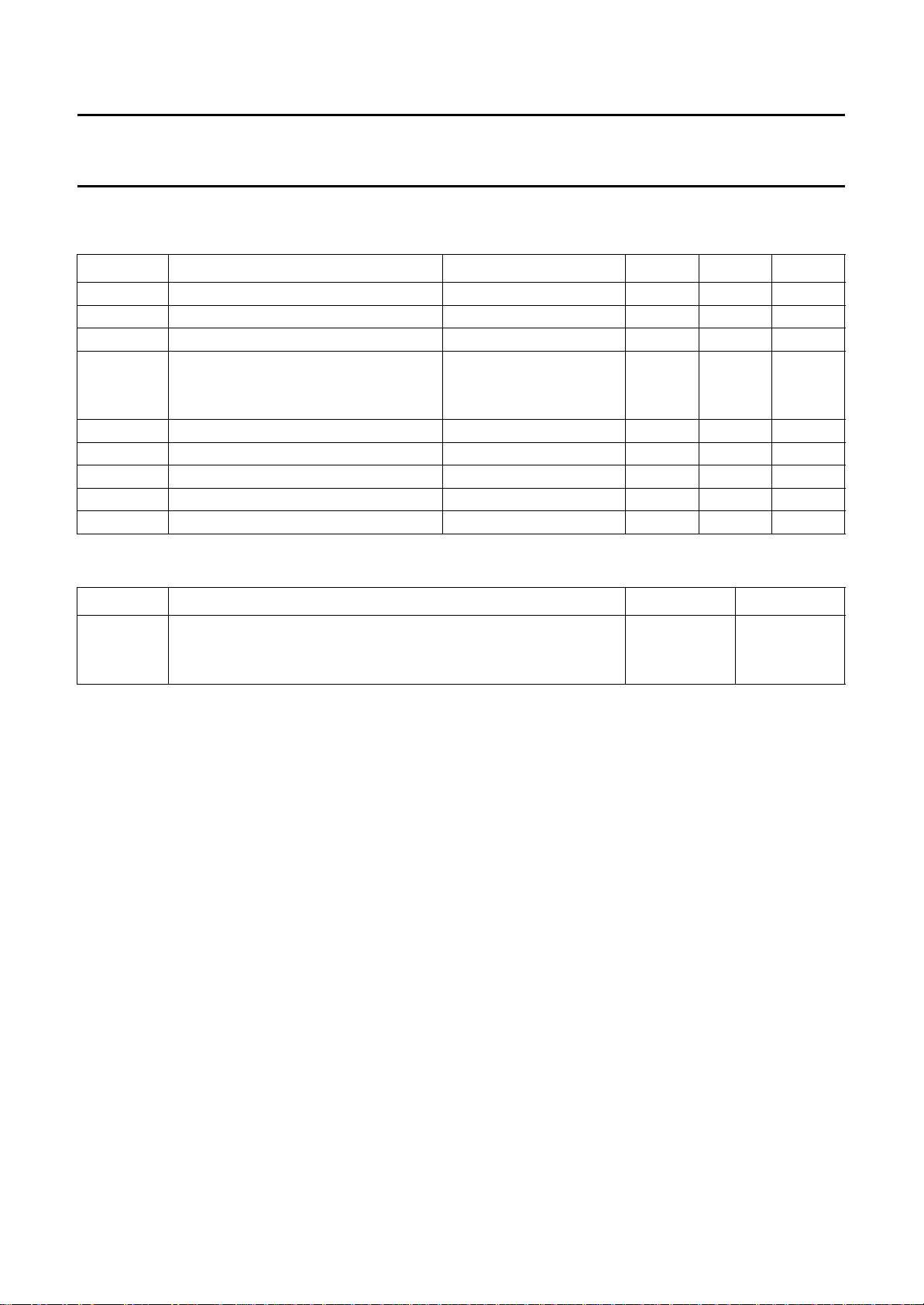
QUICK REFERENCE DATA
SYMBOL PARAMETER CONDITIONS MIN. TYP. MAX. UNIT
V
P
P
out
supply voltage 4.5 − 18 V
output power VP=6V
TDA7053A R
TDA7053AT R
G
G
I
q(tot)
v
C
voltage gain 39.5 40.5 41.5 dB
gain control 68.0 73.5 − dB
total quiescent current VP=6V; RL=∞−22 25 mA
THD total harmonic distortion
TDA7053A P
TDA7053AT P
out
out
GENERAL DESCRIPTION
The TDA7053A (2 × 1 W) and TDA7053AT (2 × 0.5 W) are
stereo BTL output amplifiers with DC volume control.
The devices are designed for use in TV and monitors, but
are also suitable for battery-fed portable recorders and
radios.
Missing Current Limiter (MCL)
A MCL protection circuit is built-in. The MCL circuit is
activated when the difference in current between the
output terminal of each amplifier exceeds 100 mA
(typical 300 mA). This level of 100 mA allows for
headphone applications (single-ended).
=8Ω 0.85 1.0 − W
L
=16Ω 0.5 0.6 − W
L
= 0.5 W − 0.3 1 %
= 0.25 W − 0.3 1 %
ORDERING INFORMATION
TYPE
NUMBER
TDA7053A DIP16
TDA7053AT SO16
NAME DESCRIPTION VERSION
plastic dual in-line package; 16 leads (300 mil); long body
plastic small outline package; 16 leads; body width 7.5 mm
1995 Nov 09 2
PACKAGE
SOT38-1
SOT162-1
Philips Semiconductors Objective specification
Stereo BTL audio output amplifier with DC
volume control
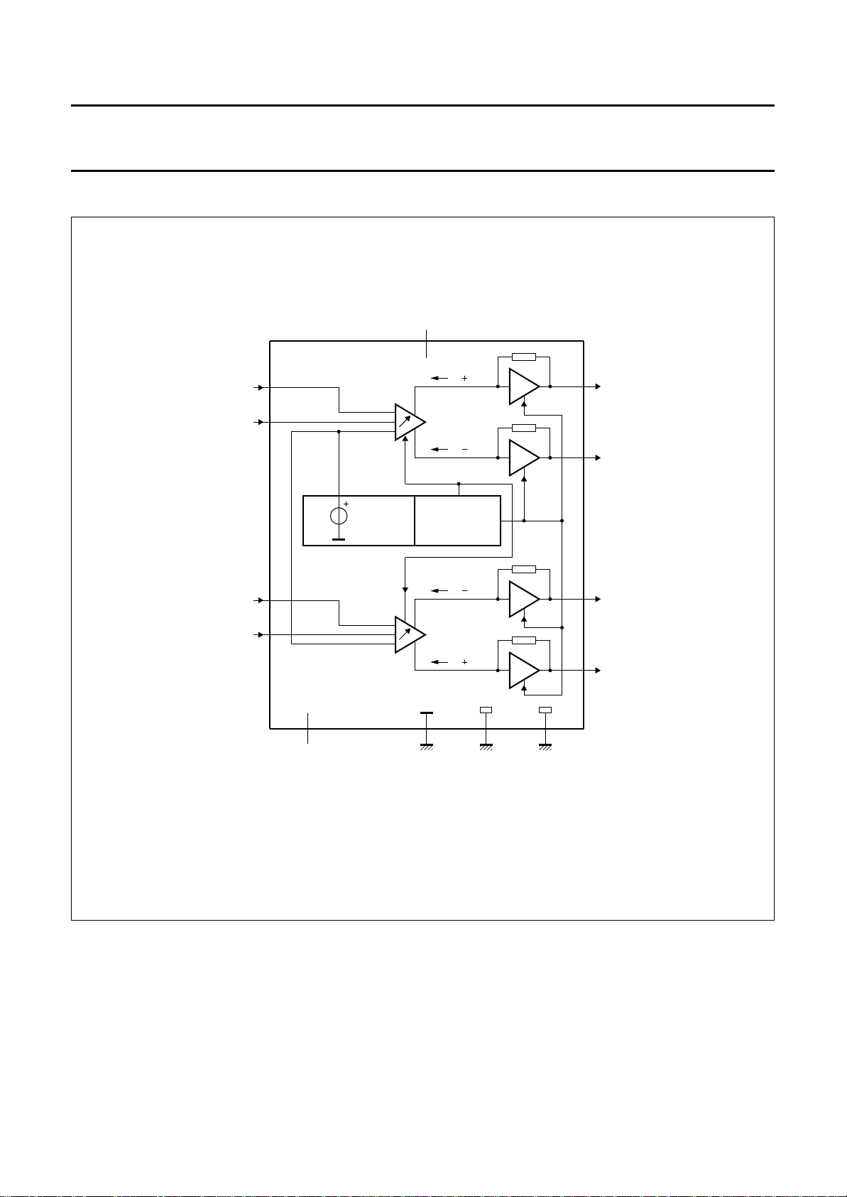
BLOCK DIAGRAM
TDA7053A
TDA7053AT
V
ref
STABILIZER
input 1
DC volume
control 1
4
2
V
P
5
I i
Ι
I i
TEMPERATURE
PROTECTION
TDA7053A
positive
16
output 1
negative
13
output 1
input 2
DC volume
control 2
6
8
not
connected
1,3,11,15
I i
ΙΙ
I i
signal
ground
power
ground 1
Fig.1 Block diagram.
12
negative
output 2
9
positive
output 2
14
107
power
ground 2
MSA717 - 2
1995 Nov 09 3
Philips Semiconductors Objective specification
Stereo BTL audio output amplifier with DC
volume control
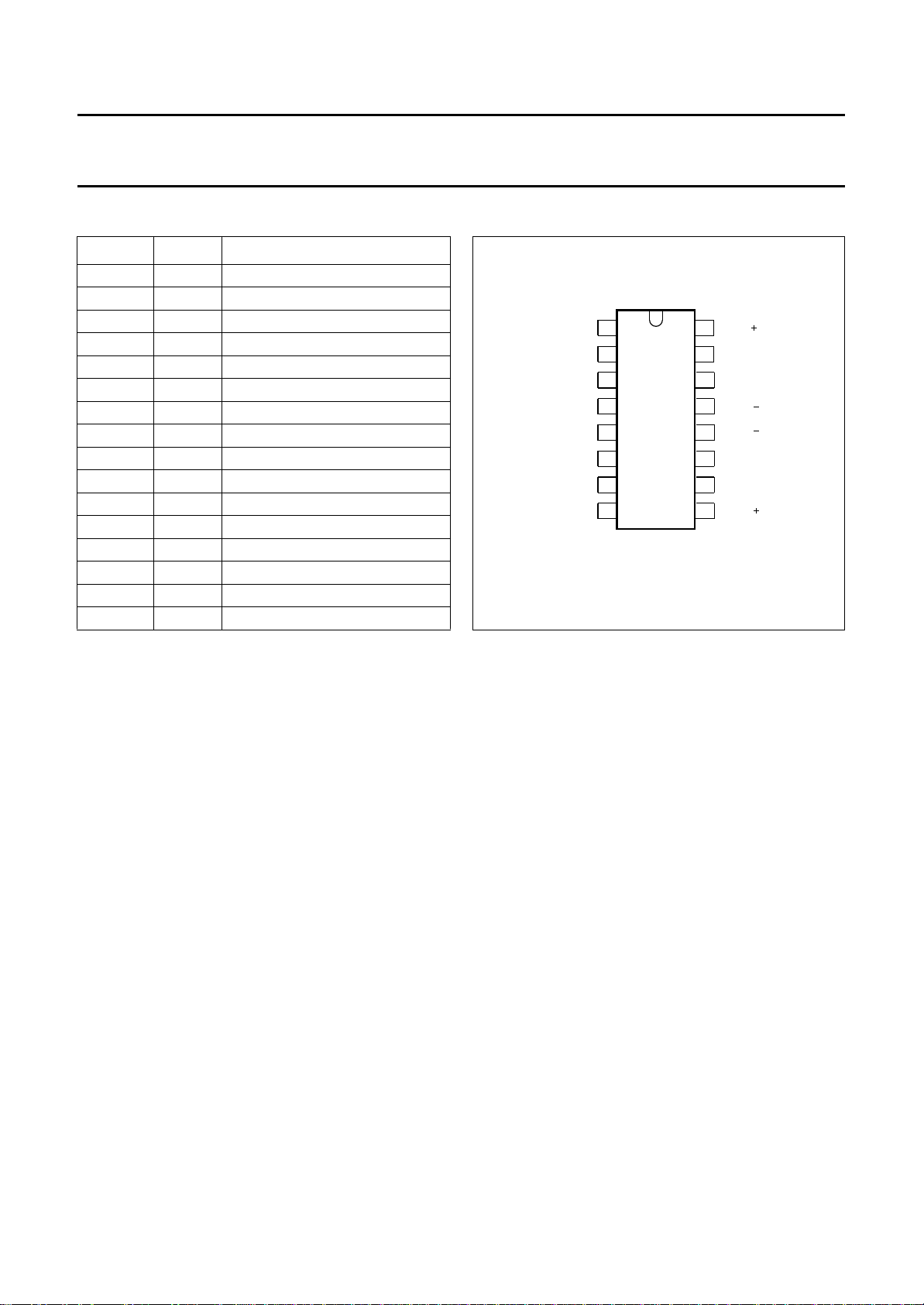
PINNING
SYMBOL PIN DESCRIPTION
n.c. 1 not connected
VC1 2 DC volume control 1
n.c. 3 not connected
V
I (1)
V
P
V
I (2)
SGND 7 signal ground
VC2 8 DC volume control 2
OUT2+ 9 positive output 2
PGND2 10 power ground 2
n.c. 11 not connected
OUT2− 12 negative output 2
OUT1− 13 negative output 1
PGND1 14 power ground 1
n.c. 15 not connected
OUT1+ 16 positive output 1
4 voltage input 1
5 positive supply voltage
6 voltage input 2
1
n.c.
2
VC1
n.c.
3
V
4
I (1)
V
V
I (2)
SGND
VC2
P
TDA7053A
TDA7053AT
5
6
7
8
MSA719 - 2
Fig.2 Pin configuration.
TDA7053A
16
OUT1
n.c.
15
PGND1
14
13
OUT1
OUT2
12
n.c.
11
PGND2
10
OUT2
9
FUNCTIONAL DESCRIPTION
The TDA7053A and TDA7053AT are stereo output
amplifiers with two DC volume control stages, designed for
TV and monitors, but also suitable for battery-fed portable
recorders and radios.
In conventional DC volume control circuits the control or
input stage is AC coupled to the output stage via external
capacitors to keep the offset voltage low.
The two DC volume control stages are integrated into the
input stages so that no coupling capacitors are required
and a low offset voltage is still maintained. The minimum
supply voltage also remains low.
The BTL principle offers the following advantages:
• Lower peak value of the supply current
• The frequency of the ripple on the supply voltage is twice
the signal frequency.
Consequently, a reduced power supply with smaller
capacitors can be used which results in cost reductions.
For portable applications there is a trend to decrease the
supply voltage, resulting in a reduction of output power at
conventional output stages. Using the BTL principle
increases the output power.
The maximum gain of the amplifier is fixed at 40.5 dB.
The DC volume control stages have a logarithmic control
characteristic. Therefore, the total gain can be controlled
from +40.5 to −33 dB.
If the DC volume control voltage falls below 0.4 V, the
device will switch to the mute mode.
The amplifier is short-circuit protected to ground, V
and
P
across the load. A thermal protection circuit is also
implemented. If the crystal temperature rises above
150 °C the gain will be reduced, thereby reducing the
output power.
Special attention is given to switch-on and switch-off
clicks, low HF radiation and a good overall stability.
1995 Nov 09 4
Philips Semiconductors Objective specification
Stereo BTL audio output amplifier with DC
TDA7053A
volume control
LIMITING VALUES
In accordance with the Absolute Maximum Rating System (IEC 134).
SYMBOL PARAMETER CONDITIONS MIN. MAX. UNIT
V
P
I
ORM
I
OSM
P
tot
t
sc
V
n
T
amb
T
stg
T
vj
THERMAL CHARACTERISTICS
supply voltage − 18 V
repetitive peak output current − 1.25 A
non-repetitive peak output current − 1.5 A
total power dissipation T
amb
≤ 25 °C
TDA7053A − 2.5 W
TDA7053AT − 1.32 W
short-circuit time − 1hr
input voltage pins 2, 4, 6 and 8 − 5V
operating ambient temperature −40 +85 °C
storage temperature −55 +150 °C
virtual junction temperature − +150 °C
SYMBOL PARAMETER VALUE UNIT
R
th j-a
thermal resistance from junction to ambient in free air
TDA7053A 50 K/W
TDA7053AT 95 K/W
Power dissipation
TDA7053A:
Assume V
= 6 V and RL=8Ω.
P
The maximum sine wave dissipation is 2 × 0.9 W = 1.8 W.
The R
of the package is 50 K/W therefore T
th j-a
amb(max)
= 150 − (50 × 1.8) = 60 °C.
TDA7053AT:
Assume V
= 6 V and RL=16Ω.
P
The maximum sine wave dissipation is 2 × 0.46 W = 0.92 W.
The R
of the package is 95 K/W therefore T
th j-a
amb(max)
= 150 − (95 × 0.92) = 62.6 °C.
1995 Nov 09 5
 Loading...