

Philips TDA7052AT-N2, TDA7052A-N2 Datasheet

DATA SH EET
Product specification
File under Integrated circuits, IC01
July 1994
INTEGRATED CIRCUITS
TDA7052A/AT
1 W BTL mono audio amplifier with
DC volume control
July 1994 2
Philips Semiconductors Product specification
1 W BTL mono audio amplifier with DC
volume control
TDA7052A/AT
FEATURES
• DC volume control
• Few external components
• Mute mode
• Thermal protection
• Short-circuit proof
• No switch-on and off clicks
• Good overall stability
• Low power consumption
• Low HF radiation
• ESD protected on all pins
GENERAL DESCRIPTION
The TDA7052A/AT are mono BTL output amplifiers with
DC volume control. They are designed for use in TV and
monitors, but also suitable for battery-fed portable
recorders and radios.
Missing Current Limiter (MCL)
A MCL protection circuit is built-in. The MCL circuit is
activated when the difference in current between the
output terminal of each amplifier exceeds 100 mA (typical
300 mA). This level of 100 mA allows for headphone
applications (single-ended).
QUICK REFERENCE DATA
ORDERING INFORMATION
Notes
1. SOT97-1; 1996 September 10.
2. SOT96-1; 1996 September 10.
SYMBOL PARAMETERS CONDITIONS MIN. TYP. MAX. UNIT
V
P
positive supply voltage range 4.5 − 18 V
P
O
output power
TDA7052A R
L
= 8 Ω; VP = 6 V 1.0 1.1 − W
TDA7052AT R
L
= 16 Ω; VP = 6 V 0.5 0.55 − W
G
v
maximum total voltage gain 34.5 35.5 36.5 dB
φ gain control range 75 80 − dB
I
P
total quiescent current VP = 6 V; RL = ∞−712mA
THD total harmonic distortion
TDA7052A P
O
= 0.5 W − 0.3 1 %
TDA7052AT P
O
= 0.25 W − 0.3 1 %
EXTENDED TYPE
NUMBER
PACKAGE
PINS PIN POSITION MATERIAL CODE
TDA7052A 8 DIL plastic SOT97
(1)
TDA7052AT 8 mini-pack plastic SOT96A
(2)
July 1994 3
Philips Semiconductors Product specification
1 W BTL mono audio amplifier with DC
volume control
TDA7052A/AT
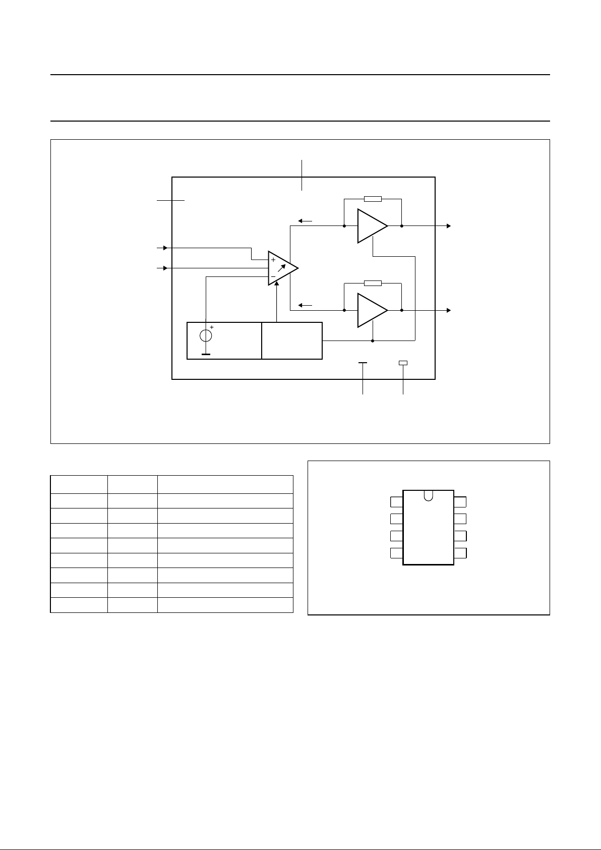
handbook, full pagewidth
positive input
6
MCD385 - 1
1
2
TDA7052A
TDA7052AT
V
P
4
5
I + i
8I – i
TEMPERATURE
PROTECTION
3
signal
ground
DC volume
control
7
n.c.
positive output
negative output
power
ground
V
ref
STABILIZER
Fig.1 Block diagram.
PINNING
SYMBOL PIN DESCRIPTION
V
P
1 positive supply voltage
IN+ 2 positive input
GND1 3 signal ground
VC 4 DC volume control
OUT+ 5 positive output
GND2 6 power ground
n.c 7 not connected
OUT− 8 negative output
handbook, halfpage
1
2
3
4
8
7
6
5
MCD384
V
P
OUT –
GND2
OUT +
GND1
IN +
VC
n.c.
TDA7052A
TDA7052AT
Fig.2 Pin configuration.
July 1994 4
Philips Semiconductors Product specification
1 W BTL mono audio amplifier with DC
volume control
TDA7052A/AT
FUNCTIONAL DESCRIPTION
The TDA7052A/AT are mono BTL output amplifiers with
DC volume control, designed for use in TV and monitors
but also suitable for battery fed portable recorders and
radios.
In conventional DC volume circuits the control or input
stage is AC coupled to the output stage via external
capacitors to keep the offset voltage low.
In the TDA7052A/AT the DC volume control stage is
integrated into the input stage so that no coupling
capacitors are required and yet a low offset voltage is
maintained. At the same time the minimum supply remains
low.
The BTL principle offers the following advantages:
• Lower peak value of the supply current
• The frequency of the ripple on the supply voltage is twice
the signal frequency.
Thus a reduced power supply with smaller capacitors can
be used which results in cost savings.
For portable applications there is a trend to decrease the
supply voltage, resulting in a reduction of output power at
conventional output stages. Using the BTL principle
increases the output power.
The maximum gain of the amplifier is fixed at 35.5 dB. The
DC volume control stage has a logarithmic control
characteristic.
The total gain can be controlled from 35.5 dB to −44 dB. If
the DC volume control voltage is below 0.3 V, the device
switches to the mute mode.
The amplifier is short-circuit proof to ground, V
P
and
across the load. Also a thermal protection circuit is
implemented. If the crystal temperature rises above
+150 °C the gain will be reduced, so the output power is
reduced.
Special attention is given to switch on and off clicks, low
HF radiation and a good overall stability.
LIMITING VALUES
In accordance with the Absolute Maximum System (IEC 134)
SYMBOL PARAMETER CONDITIONS MIN. MAX. UNIT
V
P
supply voltage range − 18 V
I
ORM
repetitive peak output current − 1.25 A
I
OSM
non-repetitive peak output current − 1.5 A
P
tot
total power dissipation T
amb
≤ 25%
TDA7052A − 1.25 W
TDA7052AT − 0.8 W
T
amb
operating ambient temperature range −40 +85 °C
T
stg
storage temperature range −55 +150 °C
T
vj
virtual junction temperature − +150 °C
T
sc
short-circuit time − 1hr
V
2
input voltage pin 2 − 8V
V
4
input voltage pin 4 − 8V
 Loading...