

Philips tda6402, tda6403 a DATASHEETS
INTEGRATED CIRCUITS
DATA SH EET
TDA6402; TDA6402A; TDA6403;
TDA6403A
5 V mixers/oscillators and
synthesizers for cable TV and VCR
2-band tuners
Product specification
Supersedes data of 1998 Jul 28
File under Integrated Circuits, IC02
2000 Jan 24

Philips Semiconductors Product specification
5 V mixers/oscillators and synthesizers for
cable TV and VCR 2-band tuners
FEATURES
• Single-chip 5 V mixer/oscillator and synthesizer for
cable TV and VCR tuners
• Synthesizer function compatible with existing TSA5526
• Universal bus protocol (I2C-bus or 3-wire bus)
– Bus protocol for 18 or 19-bit transmission (3-wire
bus)
– Extraprotocolfor 27-bit transmission(testmodes and
features for 3-wire bus)
– Address + 4 data bytes transmission (I2C-bus ‘write’
mode)
– Address + 1 status byte (I2C-bus ‘read’ mode)
– 4 independent I2C-bus addresses.
• 1 PNP buffer for UHF band selection (25 mA)
• 3 PNP buffers for general purpose, e.g. 2 VHF
sub-bands, FM sound trap (25 mA)
• 33 V tuning voltage output
• In-lock detector
• 5-step A/D converter (3 bits in I2C-bus mode)
• 15-bit programmable divider
• Programmable reference divider ratio (512, 640 or
1024)
• Programmable charge pump current (60 or 280 µA)
• Programmable automatic charge pump current switch
• Varicap drive disable
• Mixer/oscillator function compatible with existing
TDA5732
• Balanced mixer with a common emitter input for VHF
(single input)
• Balanced mixer with a common base input for UHF
(balanced input)
• 2-pin common emitter oscillator for VHF
• 4-pin common emitter oscillator for UHF
• IF preamplifier with asymmetrical 75 Ω output
impedance to drive a low-ohmic impedance (75 Ω)
• Low power
• Low radiation
• Small size
• TheTDA6402A andTDA6403Adifferfrom theTDA6402
and TDA6403 by the UHF port protocol in the I2C-bus
mode (see Tables 3 and 4).
APPLICATIONS
• Cable tuners for TV and VCR (switched concept for
VHF)
• Recommended RF bands for the USA:
55.25 to 133.25 MHz, 139.25 to 361.25 MHz and
367.25 to 801.25 MHz.
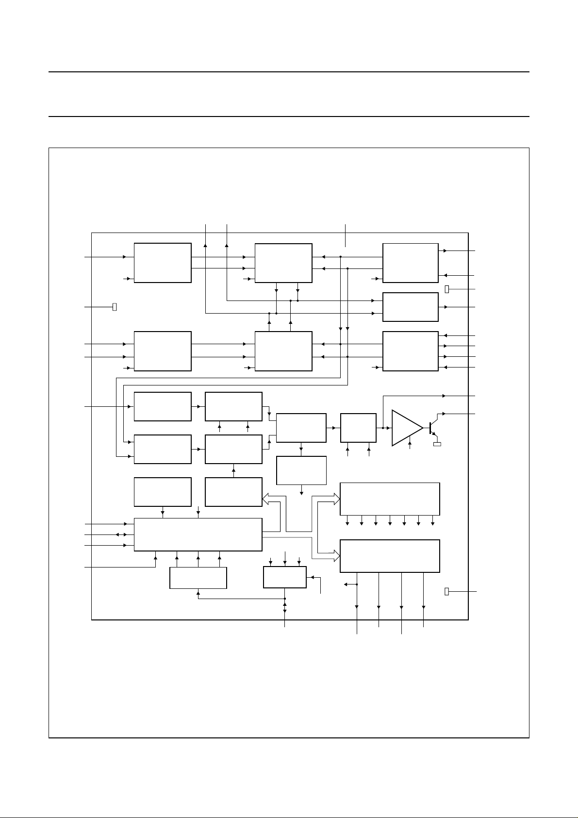
GENERAL DESCRIPTION
The TDA6402, TDA6402A, TDA6403 and TDA6403A are
programmable2-band mixers/oscillatorsand synthesizers
intended for VHF/UHF cable tuners (see Fig.1).
The devices include two double balanced mixers and two
oscillators for the VHF and UHF band respectively, an IF
amplifier and a PLL synthesizer. The VHF band can be
split-up into two sub-bands using a proper oscillator
application and a switchable inductor. Two pins are
available between the mixer output and the IF amplifier
input to enable IF filtering for improved signal handling.
Four PNP ports are provided. Band selection is provided
by using pin PUHF. When PUHF is ‘ON’, the UHF
mixer-oscillator is active andthe VHFband isswitched off.
When PUHF is ‘OFF’, the VHF mixer-oscillator is active
and the UHF band is ‘OFF’. PVHFL and PVHFH areused
to select the VHF sub-bands. FMST is a general purpose
port, that can be used to switch an FM sound trap. When
itis used,thesum ofthe collector currentshas tobelimited
to 30 mA.
The synthesizer consists of a divide-by-eight prescaler, a
15-bit programmable divider, a crystal oscillator and its
programmable reference divider and a phase/frequency
detector combined with a charge pump which drives the
tuning amplifier, including 33 V output (V33) at pin VT.
Depending on the reference divider ratio (512, 640 or
1024), the phase comparator operates at 7.8125 kHz,
6.25 kHz or 3.90625 kHz with a 4 MHz crystal.
TDA6402; TDA6402A;
TDA6403; TDA6403A
2000 Jan 24 2
Philips Semiconductors Product specification
5 V mixers/oscillators and synthesizers for
cable TV and VCR 2-band tuners
The device can be controlled according to the I2C-bus
format or 3-wire bus format depending on the voltage
applied to pin SW (see Table 2). In the 3-wire bus mode
(SW = HIGH), pin LOCK/ADC is the LOCK output.
The LOCK output is LOW when the PLL loop is locked.
In the I2C-bus mode(SW = LOW), the lockdetector bit FL
is set tologic 1 when the loop is locked and is read on the
SDA line (Status Byte; SB) during a READ operation in
I2C-bus mode only. The Analog-to-Digital Converter
(ADC) input isavailable on pin LOCK/ADC for digitalAFC
control in the I2C-bus mode only. The ADC code is read
during a READ operation on the I2C-bus (see Table 11).
In test mode,pin LOCK/ADC isused as aTEST outputfor
f
and1⁄2f
REF
(see Table 7).
When the automatic charge pump current switch mode is
activated and when the loop is phase-locked, the charge
pumpcurrent valueisautomatically switchedto LOW.This
action is taken to improve the carrier-to-noise ratio.
The status of this feature can be read in the ACPS flag
during a READ operation on the I2C-bus (see Table 9).
,in bothI2C-busmode and3-wirebus mode
DIV
TDA6402; TDA6402A;
TDA6403; TDA6403A
2
C-bus mode (SW = GND)
I
Five serial bytes (including address byte) are required to
address the device, select the VCO frequency, program
the four ports, set the charge pump current and set the
reference divider ratio. The device has four independent
I2C-bus addresses which can be selected by applying a
specific voltage on input CE (see Table 6).
3-wire bus mode (SW = OPEN or VCC)
Data is transmitted to the devices during a HIGH-level on
inputCE (enableline). The deviceis compatiblewith 18-bit
and19-bit dataformats,as showninFigs 4 and 5. Thefirst
four bits are used to program the PNP ports and the
remaining bits control the programmable divider. A 27-bit
data format may also be used to set the charge pump
current, the reference divider ratio and for test purposes
(see Fig.6).
It is not allowed to address the devices with words whose
length is different from 18, 19 or 27 bits.
Table 1 Data word length for 3-wire bus
(1)
TYPE NUMBER DATA WORD REFERENCE DIVIDER
TDA6402; TDA6402A; TDA6403; TDA6403A 18-bit 512 62.50 kHz
TDA6402; TDA6402A; TDA6403; TDA6403A 19-bit 1024 31.25 kHz
TDA6402; TDA6402A; TDA6403; TDA6403A 27-bit programmable programmable
Note
1. The selectionof the referencedivider is givenby an automaticidentification of thedata word length.When the 27-bit
format is used, the reference divider is controlled by RSA and RSB bits (see Table 8). More details are given in
Chapter “PLL functional description”, Section “3-wire bus mode (SW = OPEN or V
CC
)”.
FREQUENCY STEP
2000 Jan 24 3
Philips Semiconductors Product specification
2
5 V mixers/oscillators and synthesizers for
cable TV and VCR 2-band tuners
TDA6402; TDA6402A;
TDA6403; TDA6403A
QUICK REFERENCE DATA
Measured over full voltage and temperature ranges; unless otherwise specified.
SYMBOL PARAMETER CONDITIONS MIN. TYP. MAX. UNIT
V
CC
I
CC
f
XTAL
I
o(PNP)
P
tot
T
stg
T
amb
f
RF
supply voltage operating 4.5 5 5.5 V
supply current all PNP ports are ‘OFF’ − 71 − mA
crystal oscillator input frequency 3.2 4.0 4.48 MHz
PNP port output current note 1 −−30 mA
total power dissipation note 2 −−490 mW
IC storage temperature −40 − +150 °C
ambient temperature −20 − +85 °C
RF frequency VHF band 55.25 − 361.25 MHz
UHF band 367.25 − 801.25 MHz
G
V
voltage gain VHF band − 19 − dB
UHF band − 29 − dB
NF noise figure VHF band − 8.5 − dB
UHF band − 9 − dB
V
o
output voltage causing 1% cross
modulation in channel
VHF band − 108 − dBµV
UHF band − 108 − dBµV
Notes
1. One buffer ‘ON’, Io= 25 mA; two buffers ‘ON’, maximum sum of Io= 30 mA.
2. The power dissipation is calculated as follows:
P
tot
V
CCICCIo
–()V
ORDERING INFORMATION
PACKAGE
TYPE NUMBER
NAME DESCRIPTION VERSION
TDA6402M;
SSOP28 plastic shrink small outline package; 28 leads; body width 5.3 mm SOT341-1
TDA6402AM
TDA6403M;
SSOP28 plastic shrink small outline package; 28 leads; body width 5.3 mm SOT341-1
TDA6403AM
CE(sat PNP)Io
1
V33
-- -
2
+×+×=
----------------------22 kΩ
2000 Jan 24 4
Philips Semiconductors Product specification
5 V mixers/oscillators and synthesizers for
cable TV and VCR 2-band tuners
BLOCK DIAGRAM
handbook, full pagewidth
VHFIN
RFGND
UHFIN1
UHFIN2
3 (26)
4 (25)
1 (28)
2 (27)
BS
RF INPUT
VHF
TDA6402
TDA6402A
TDA6403
TDA6403A
RF INPUT
UHF
IFFIL1 IFFIL2
5 (24)
6 (23)
BS
BSBS
VHF
MIXER
UHF
MIXER
V
CC
19 (10)
TDA6402; TDA6402A;
TDA6403; TDA6403A
(5) 24
VHF
BS
BS
OSCILLATOR
IF
PREAMPLIFIER
UHF
OSCILLATOR
(7) 22
(6) 23
(9) 20
(1) 28
(2) 27
(3) 26
(4) 25
VHFOSCOC
VHFOSCIB
OSCGND
IFOUT
UHFOSCIB2
UHFOSCOC2
UHFOSCOC1
UHFOSCIB1
XTAL
CL
DA
SW
CE/AS
18 (11)
14 (15)
13 (16)
11 (18)
12 (17)
XTAL
OSCILLATOR
4 MHz
PRESCALER
DIVIDE BY 8
POWER-DOWN
DETECTOR
SCL
2
SDA
I
C / 3-WIRE BUS TRANSCEIVER
SW
CE/AS
3-BIT A/D
CONVERTER
PRESCALER
DIVIDE BY
512, 640, 1024
RSA RSB
15-BIT
PROGRAMMABLE
DIVIDER
15-BIT
FREQUENCY
REGISTER
FL
f
REF
COMPARATOR
f
DIV
IN LOCK
DETECTOR
f
REF
1/2f
FL
GATE
15 (14)
LOCK/ADC
PHASE
FL
DIV
T0, T1, T2
CHARGE
PUMP
T0, T1, T2 CP
CP T2 T1 T0 RSA RSB OS
UHF VHFH VHFL FMST
BS
9 (20)
PUHF
CONTROL
REGISTER
PORT
REGISTER
8 (21)
PVHFH
OPAMP
OS
7 (22)
PVHFL
FMST
10 (19)
(13) 16
(12) 17
(8) 21
MGE692
CP
VT
GND
The pin numbers in parenthesis represent the TDA6403 and TDA6403A.
Fig.1 Block diagram.
2000 Jan 24 5
Philips Semiconductors Product specification
5 V mixers/oscillators and synthesizers for
cable TV and VCR 2-band tuners
PINNING
PIN
SYMBOL
UHFIN1 1 28 UHF RF input 1
UHFIN2 2 27 UHF RF input 2
VHFIN 3 26 VHF RF input
RFGND 4 25 RF ground
IFFIL1 5 24 IF filter output 1
IFFIL2 6 23 IF filter output 2
PVHFL 7 22 PNP port output, general purpose (e.g. VHF low sub-band)
PVHFH 8 21 PNP port output, general purpose (e.g. VHF high sub-band)
PUHF 9 20 PNP port output, UHF band
FMST 10 19 PNP port output, general purpose (e.g. FM sound trap)
SW 11 18 bus mode selection input (I
CE/AS 12 17 Chip Enable/Address Selection input
DA 13 16 serial data input/output
CL 14 15 serial clock input
LOCK/ADC 15 14 lock detector output (3-wire bus)/ADC input (I
CP 16 13 charge pump output
VT 17 12 tuning voltage output
XTAL 18 11 crystal oscillator input
V
CC
IFOUT 20 9 IF output
GND 21 8 digital ground
VHFOSCIB 22 7 VHF oscillator input base
OSCGND 23 6 oscillator ground
VHFOSCOC 24 5 VHF oscillator output collector
UHFOSCIB1 25 4 UHF oscillator input base 1
UHFOSCOC1 26 3 UHF oscillator output collector 1
UHFOSCOC2 27 2 UHF oscillator output collector 2
UHFOSCIB2 28 1 UHF oscillator input base 2
TDA6402;
TDA6402A
19 10 supply voltage
TDA6403;
TDA6403A
TDA6402; TDA6402A;
TDA6403; TDA6403A
DESCRIPTION
2
C-bus/3-wire bus)
2
C-bus)
2000 Jan 24 6
Philips Semiconductors Product specification
5 V mixers/oscillators and synthesizers for
cable TV and VCR 2-band tuners
handbook, halfpage
UHFIN1
UHFIN2
VHFIN
RFGND
IFFIL1
IFFIL2
PVHFL
PVHFH
PUHF
FMST
SW
CE/AS
DA
CL
1
2
3
4
5
6
7
TDA6402A
8
9
10
11
12
13
TDA6402
MGE690
UHFOSCIB2
28
UHFOSCOC2
27
UHFOSCOC1
26
UHFOSCIB1
25
VHFOSCOC
24
23
OSCGND
VHFOSCIB
22
21
GND
IFOUT
20
V
19
CC
XTAL
18
VT
17
CP
16
1514
LOCK/ADC
handbook, halfpage
UHFOSCIB2
UHFOSCOC2
UHFOSCOC1
UHFOSCIB1
VHFOSCOC
VHFOSCIB
LOCK/ADC
OSCGND
GND
IFOUT
V
CC
XTAL
VT
CP
TDA6402; TDA6402A;
TDA6403; TDA6403A
1
2
3
4
5
6
7
TDA6403A
8
9
10
11
12
13
TDA6403
MGE691
28
27
26
25
24
23
22
21
20
19
18
17
16
1514
UHFIN1
UHFIN2
VHFIN
RFGND
IFFIL1
IFFIL2
PVHFL
PVHFH
PUHF
FMST
SW
CE/AS
DA
CL
Fig.2 Pin configurationfor TDA6402 and
TDA6402A.
PLL FUNCTIONAL DESCRIPTION
The device is controlled via the I2C-bus or the 3-wire bus,
depending on the voltage applied on the SW input.
A HIGH-level on the SW input enables the 3-wire bus;
and clock inputs respectively. A LOW-level on SW input
enables the I2C-bus; the CE/AS, DA and CL inputs are
used as address selection (AS), SDA and SCL input
respectively (see Table 2).
Fig.3 Pin configurationfor TDA6403 and
TDA6403A.
CE/AS, DA and CL inputs are used as enable (CE), data
Table 2 Bus mode selection
PIN
SYMBOL
TDA6402;
TDA6402A
TDA6403;
TDA6403A
3-WIRE BUS MODE I2C-BUS MODE
SW 11 18 HIGH-level or OPEN LOW-level or GND
CE/AS 12 17 enable input address selection input
DA 13 16 data input serial data input
CL 14 15 clock input serial clock input
LOCK/ADC 15 14 LOCK/TEST output ADC input/TEST output
2000 Jan 24 7
Philips Semiconductors Product specification
5 V mixers/oscillators and synthesizers for
cable TV and VCR 2-band tuners
I2C-bus mode (SW = GND)
WRITE MODE; R/W = 0 (see Tables 3 and 4)
Data bytes can be sent to the device after the address
transmission (first byte). Four data bytes are needed to
fully program the device. The bus transceiver has an
auto-increment facility which permits the programming of
the device within one single transmission
(address + 4 data bytes).
The device can also be partially programmed providing
that the first data byte following the address is divider
byte 1 (DB1) or control byte (CB). The bits in the data
bytes aredefined inTables 3 and 4. The firstbit ofthe first
data byte transmitted indicates whether frequency data
(first bit = 0) or control and band-switch data (first bit = 1)
will follow.Until an I2C-bus STOPcommand is sent by the
Table 3 I2C-bus data format, ‘write’ mode for the TDA6402 and TDA6403
NAME BYTE
MSB LSB
Address byte ADB 11000MA1MA0R/W=0A
Divider byte 1 DB1 0 N14 N13 N12 N11 N10 N9 N8 A
Divider byte 2 DB2 N7 N6 N5 N4 N3 N2 N1 N0 A
Control byte CB 1 CP T2 T1 T0 RSA RSB OS A
Band-switch byte BB XXXXFMST PUHF PVHFH PVHFL A
controller,additional databytes canbe entered withoutthe
need to re-address the device. The frequency register is
loaded after the8th clock pulse of thesecond divider byte
(DB2), the control register is loaded after the 8th clock
pulse ofthe controlbyte (CB)and theband-switch register
is loaded after the 8th clock pulse of the band switch byte
(BB).
I2C-BUS ADDRESS SELECTION
The moduleaddress contains programmableaddress bits
(MA1 and MA0) which offer the possibility of having
several synthesizers(up to 4) inone system byapplying a
specific voltageon theCE input.The relationshipbetween
MA1 and MA0 and the input voltage applied to the CE
input is given in Table 6.
BITS
TDA6402; TDA6402A;
TDA6403; TDA6403A
ACK
2
Table 4 I
Address byte ADB 11000MA1MA0R/W=0A
Divider byte 1 DB1 0 N14 N13 N12 N11 N10 N9 N8 A
Divider byte 2 DB2 N7 N6 N5 N4 N3 N2 N1 N0 A
Control byte CB 1 CP T2 T1 T0 RSA RSB OS A
Band-switch byte BB XXXXPUHF FMST PVHFH PVHFL A
2000 Jan 24 8
C-bus data format, ‘write’ mode for the TDA6402A and TDA6403A
NAME BYTE
MSB LSB
BITS
ACK
Philips Semiconductors Product specification
5 V mixers/oscillators and synthesizers for
cable TV and VCR 2-band tuners
Table 5 Description of symbols used in Tables 3 and 4
SYMBOL DESCRIPTION
A acknowledge
MA1, MA0 programmable address bits (see Table 6)
N14 to N0 programmable divider bits; N = N14 × 2
CP charge pump current:
CP=0=60µA
CP = 1 = 280 µA (default)
T2, T1,T0 test bits (see Table 7)
RSA, RSB reference divider ratio select bits (see Table 8)
OS tuning amplifier control bit:
OS = 0; normal operation; tuning voltage is ‘ON’ (default)
OS = 1; tuning voltage is ‘OFF’ (high-impedance)
PVHFL, PVHFH, PUHF, FMST PNP ports control bits:
bit = 0; buffer n is ‘OFF’ (default)
bit = 1; buffer n is ‘ON’
X don’t care
14
+ N13 × 213+ ... + N1 × 21+N0
TDA6402; TDA6402A;
TDA6403; TDA6403A
Table 6 Address selection (I
2
C-bus mode)
MA1 MA0 VOLTAGE APPLIED ON CE INPUT (SW = GND)
0 0 0Vto0.1×V
0 1 open or 0.2 × VCCto 0.3 × V
1 0 0.4 × VCCto 0.6 × V
1 1 0.9 × VCCto 1.0 × V
CC
CC
CC
CC
Table 7 Test modes
T2 T1 T0 TEST MODES
0 0 0 automatic charge pump switched off
0 0 1 automatic charge pump switched on (note 1)
0 1 X charge pump is ‘OFF’
1 1 0 charge pump is sinking current
1 1 1 charge pump is sourcing current
100f
101
is available on pin LOCK/ADC (note 2)
REF
1
⁄
f
is available on pin LOCK/ADC (note 2)
2
DIV
Notes
1. This is the default mode at power-on reset.
2. The ADCinput cannot beused when these testmodes are active;see Section “Read mode;R/W = 1 (see Table 9)”
for more information.
2000 Jan 24 9

Philips Semiconductors Product specification
5 V mixers/oscillators and synthesizers for
cable TV and VCR 2-band tuners
Table 8 Reference divider ratio select bits
RSA RSB REFERENCE DIVIDER RATIO FREQUENCY STEP (kHz)
(1)
X
0 1 1024 3.90625
1 1 512 7.8125
Note
1. X = don’t care.
READ MODE; R/W = 1 (see Table 9)
Data canbe read from the device by settingthe R/W bit to
logic 1. After the slave address has been recognized, the
device generates an acknowledge pulse and the first data
byte (status byte) is transferred on the SDA line (MSB
first). Data is valid on the SDA line during a HIGH-level of
theSCL clocksignal. Asecond databyte canbe readfrom
the device if the microcontroller generates an
acknowledge on the SDA line (master acknowledge).
End of transmission will occur if no master acknowledge
occurs. The device will then release the data line to allow
the microcontroller to generate a STOP condition.
The PORflag isset to logic 1at power-on.Theflag isreset
when an end-of-data is detected by the device (end of a
0 640 6.25
TDA6402; TDA6402A;
TDA6403; TDA6403A
READ sequence). Control of the loop is made possible
with the in-lock flag FL which indicates when the loop is
locked (FL = 1).
The automatic charge pump switch flag (ACPS) is LOW
when theautomatic chargepump switchmode is ‘ON’ and
the loop is locked. In other conditions, ACPS = 1.
When ACPS = 0, thecharge pump currentis forced to the
LOW value.
A built-in ADC is available on LOCK/ADC pin (I2C-bus
mode only). This converter can be used to apply AFC
informationto themicrocontroller fromthe IFsection ofthe
television.The relationshipbetween thebitsA2, A1andA0
is given in Table 11.
Table 9 Read data format
NAME BYTE
Address byte ADB 11000MA1MA0R/W=1A
Status byte SB POR FL ACPS 1 1 A2 A1 A0 −
Note
1. MSB is transmitted first.
Table 10 Description of symbols used in Table 9
SYMBOL DESCRIPTION
A acknowledge
POR power-on reset flag (POR = 1 at power-on)
FL in-lock flag (FL = 1 when the loop is locked)
ACPS automatic charge pump switch flag:
ACPS = 0; active
ACPS = 1; not active
A2, A1, A0 digital outputs of the 5-level ADC
MSB
(1)
BITS
ACK
LSB
2000 Jan 24 10
Philips Semiconductors Product specification
5 V mixers/oscillators and synthesizers for
cable TV and VCR 2-band tuners
Table 11 A to D converter levels (note 1)
A2 A1 A0 VOLTAGE APPLIED ON ADC INPUT
1 0 0 0.60 × VCCto 1.00 × V
0 1 1 0.45 × VCCto 0.60 × V
0 1 0 0.30 × VCCto 0.45 × V
0 0 1 0.15 × VCCto 0.30 × V
0 0 0 0 to 0.15 × V
Note
1. Accuracy is ±0.03 × V
POWER-ON RESET
Table 12 Default bits at power-on reset
NAME BYTE
Address byte ADB 1 1 0 0 0 MA1 MA0 X
Divider byte 1 DB1 0 XXXXXXX
Divider byte 2 DB2 XXXXXXXX
Control byte CB 1 1 0 0 1 X 1 1
Band switch byte BB XXXX0000
CC
.
MSB LSB
CC
BITS
TDA6402; TDA6402A;
TDA6403; TDA6403A
CC
CC
CC
CC
The power-on detection threshold voltage V
VCC= 2 V at room temperature. Below this threshold, the
device is reset to the power-on state.
At power-on state, the charge pump current is set to
280 µA, the tuning voltage outputis disabled, the test bits
T2, T1 and T0 are set to ‘001’ (automatic charge pump
switch ‘ON’) and RSB is set to logic 1.
PUHF is ‘OFF’, which means that the UHF oscillator and
the UHF mixer are switched off. Consequently, the VHF
oscillator andthe VHF mixer areswitched on. PVHFL and
PVHFH are ‘OFF’, which means that the VHF tank circuit
is working in the VHF I sub-band. The tuning amplifier is
switched off until the first transmission. In that case, the
tank circuit in VHF I is supplied with the maximum tuning
voltage. The oscillator is therefore working at the end of
the VHF I sub-band.
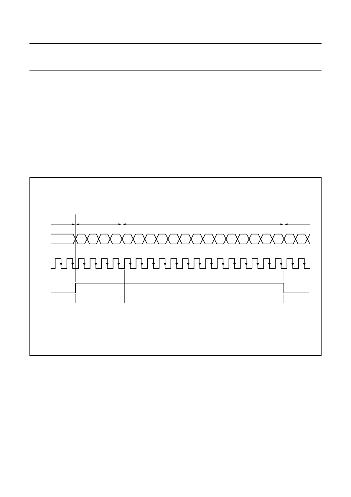
3-wire bus mode (SW = OPEN or VCC)
Duringa HIGH-levelon theCEinput (enableline), thedata
is clocked into the data register at the HIGH-to-LOW
transition of the clock. The first four bits control the PNP
ports and areloaded into the internal band switchregister
on the 5th rising edge of the clock pulse. The frequency
POR
is set to
bits are loaded into the frequency register at the
HIGH-to-LOW transition of the chip enable line when an
18-bit or 19-bit data word is transmitted(see Figs 4 and 5).
When a27-bit data word istransmitted, the frequency bits
are loaded into the frequency register on the 20th rising
edge of the clock pulse and the control bits at the
HIGH-to-LOWtransition ofthechip enableline (seeFig.6).
Inthis mode,the referencedivider isgiven bythe RSA and
RSB bits (see Table 8). The test bits T2, T1 and T0, the
charge pump bit CP, the ratio select bit RSB and the OS
bit can only be selected or changed with a 27-bit
transmission. They remain programmed if an 18-bit or
19-bit transmission occurs. Only RSA is controlled by the
transmission length when the 18-bit or 19-bit format is
used. When an 18-bit data word is transmitted, the most
significant bit of the divider N14 is internally set to logic 0
and the RSA bit is set to logic 1. When a 19-bit data word
is transmitted, the RSA bit is set to logic 0.
A data word of less than 18 bits will not affect the
frequency register of the device. The definition of the bits
is unchanged compared to I2C-bus mode.
It is not allowed to address the devices with words whose
length is different from 18, 19 or 27 bits.
2000 Jan 24 11
Philips Semiconductors Product specification
5 V mixers/oscillators and synthesizers for
cable TV and VCR 2-band tuners
POWER-ON RESET
The power-on detection threshold voltage V
VCC= 2 V at room temperature. Below this threshold, the
device is reset to the power-on state.
At power-on state, the charge pump current is set to
280 µA, the tuning voltage outputis disabled, the test bits
T2, T1 and T0 are set to ‘001’ (automatic charge pump
switch ‘ON’) and RSB is set to logic 1.
PUHF is ‘OFF’, which means that the UHF oscillator and
the UHF mixer are switched off. Consequently, the VHF
oscillator andthe VHF mixer areswitched on. PVHFL and
handbook, full pagewidth
INVALID
DATA
DA
BAND SWITCH
DATA
FMST
PUHF
PVHFL
PVHFH
N13 N12 N11 N10 N9 N8 N7 N6 N5 N4 N3 N2 N1 N0
POR
is set to
TDA6402; TDA6402A;
TDA6403; TDA6403A
PVHFH are ‘OFF’, which means that the VHF tank circuit
is working in the VHF I sub-band. The tuning amplifier is
switched off until the first transmission. In that case, the
tank circuit in VHF I is supplied with the maximum tuning
voltage. The oscillator is therefore working at the end of
the VHF I sub-band.
If the first sequence transmitted to the device
has 18 or 19 bits, the reference divider ratio is set to 512
or 1024, depending on the sequence length.
If the sequence has 27 bits, the reference divider ratio is
fixed by RSA and RSB bits (see Table 8).
FREQUENCY
DATA
INVALID
DATA
CL
CE
145 18
LOAD BAND SWITCH
REGISTER
LOAD FREQUENCY
REGISTER
Fig.4 Normal mode; 18-bit data format (RSA = 1).
MGE693
2000 Jan 24 12
 Loading...