

Philips tda6120q DATASHEETS

INTEGRATED CIRCUITS
DATA SH EET
TDA6120Q
Video output amplifier
Preliminary specification
Supersedes data of 1997 Jul 17
File under Integrated Circuits, IC02
1997 Aug 27

Philips Semiconductors Preliminary specification
Video output amplifier TDA6120Q
FEATURES
• High large signal bandwidth of 32 MHz (typ.) at
125 V (p-p)
• High small signal bandwidth of 47 MHz (typ.) at
60 V (p-p)
• Rise/fall time of 12.5 ns for 125 V (p-p)
• High slew rate of 10 V/ns
• Low static power dissipation of 2.5 W at 200 V supply
voltage
• High maximum output voltage
• Bandwidth independent of voltage gain
• Maximum overall voltage gain over 46 dB
• High Power Supply Rejection Ratio (PSRR)
• Fast cathode current measurement output for dark
current control loop
• Differential voltage input.
ORDERING INFORMATION
TYPE
NUMBER
TDA6120Q DBS13P plastic DIL-bent-SIL power package; 13 leads (lead length 7.7 mm) SOT141-8
NAME DESCRIPTION VERSION
GENERAL DESCRIPTION
The TDA6120Q is a single 30 MHz, 125 V (p-p) video
output amplifier contained in a plastic DIL-bent-SIL power
package.The device uses high-voltage DMOS technology
and is intended to drive the cathodes of a CRT in High
Definition TVs (HDTVs) or monitors.
PACKAGE
1997 Aug 27 2
Philips Semiconductors Preliminary specification
Video output amplifier TDA6120Q
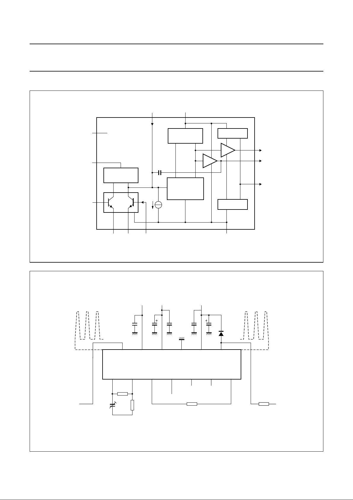
BLOCK DIAGRAM
handbook, full pagewidth
n.c.
V
CC
VIN−
9, 11
6
2
TDA6120Q
MIRROR
1×
in out
1
RC+
RC−
IIN
5
0.7 pF
+
5 mA
J
3
4
VIN+
V
MIRROR
in out
out 1×
in
CURRENT
INPUT
4×
DD
10
out 4×
CASCODE
1×
1×
CASCODE
8
GND
12
13
MGK440
OUTC
OUT
7
OUTM
Fig.1 Block diagram.
handbook, full pagewidth
V
C
r
10 nF
VIN− VIN+
2
+12 V
ref
C
CC
10
µF
4 6 8 10 12
C
22
nF
V
CC
TDA6120Q
1
C1
68 pF
35791113
RC−
442 Ω
RC+
R
i
R
22 Ω
IIN OUTM n.c. n.c.
ia
Fig.2 Top view.
1997 Aug 27 3
+200 V
C
C
D
22
nF
R
f
22 kΩ
C
DD
3.3
µF
D
flash
V
DD
OUTCGND
OUT
R
flash
147 Ω
CRTVIN
MGK441

Philips Semiconductors Preliminary specification
Video output amplifier TDA6120Q
PINNING
SYMBOL PIN DESCRIPTION
RC− 1 inverting input pre-emphasis
network
VIN− 2 inverting voltage input
RC+ 3 non-inverting input pre-emphasis
network
VIN+ 4 non-inverting voltage input
IIN 5 feedback current input
V
CC
6 low supply voltage (12 V)
OUTM 7 cathode current measurement
output
GND 8 power ground and heatsink
n.c. 9 not connected
V
DD
10 high supply voltage (200 V)
n.c. 11 not connected
OUTC 12 cathode output
OUT 13 feedback output
handbook, halfpage
RC−
VIN−
RC+
VIN+
IIN
V
CC
OUTM
GND
n.c.
V
DD
n.c.
OUTC
OUT
1
2
3
4
5
6
7
TDA6120Q
8
9
10
11
12
13
MGK438
Fig.3 Pin configuration.
LIMITING VALUES
In accordance with the Absolute Maximum Rating System (IEC 134).
SYMBOL PARAMETER CONDITIONS MIN. MAX. UNIT
V
DD
V
CC
V
i
V
i(dif)
V
i(pe)
V
i(dif)(pe)
high supply voltage 0 280 V
low supply voltage 0 20 V
input voltage (pins 2 and 4) 0 V
differential mode input voltage (pins 2 and 4) −V
CC
pre-emphasis input voltage (pins 1 and 3) 0 V
differential mode pre-emphasis input voltage
−V
CC
CC
V
CC
CC
V
CC
V
V
V
V
(pins 1 and 3)
V
IIN
V
OUTM
V
o
T
stg
T
j
V
ESD
input voltage (pin 5) 0 2V
BE
V
measurement output voltage 0 20 V
output voltage (pins 12 and 13) 0 V
DD
V
storage temperature −55 +150 °C
junction temperature −20 +150 °C
voltage peak human body model note 1 − 2000 V
voltage peak machine model − 300 V
Note
1. 1250 V for IIN (pin 5).
1997 Aug 27 4

Philips Semiconductors Preliminary specification
Video output amplifier TDA6120Q
(1) Infinite heatsink.
(2) No heatsink.
QUALITY SPECIFICATION
20
handbook, halfpage
P
tot
(W)
16
12
8
4
0
−20 160
(1)
(2)
04020 80 120
T
amb
Fig.4 Power derating curve.
MGK442
(°C)
Quality specification in accordance with
“SNW-FQ-611 part E”
.
THERMAL CHARACTERISTICS
SYMBOL PARAMETER VALUE UNIT
R
th j-c
thermal resistance from junction to case 3.0 K/W
1997 Aug 27 5
 Loading...