

Philips TDA6108JF-N1 Datasheet

DATA SH EET
Product specification
Supersedes data of 1998 Jun 22
File under Integrated Circuits, IC02
1999 Oct 29
INTEGRATED CIRCUITS
TDA6108JF
Triple video output amplifier
1999 Oct 29 2
Philips Semiconductors Product specification
Triple video output amplifier TDA6108JF
FEATURES
• Typical bandwidth of 9.0 MHz for an output signal of
60 V (p-p)
• High slew rate of 1850 V/µs
• No external components required
• Very simple application
• Single supply voltage of 200 V
• Internal reference voltage of 2.5 V
• Fixed gain of 51
• Black-Current Stabilization (BCS) circuit
• Thermal protection.
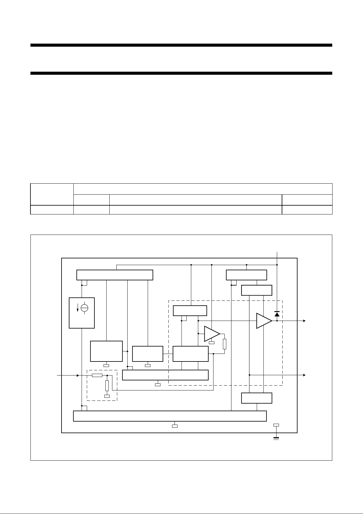
GENERAL DESCRIPTION
The TDA6108JF includes three video output amplifiers in
oneplasticDIL-bent-SIL9-pinmediumpower(DBS9MPF)
package (SOT111-1), using high-voltage DMOS
technology, and is intended to drive the three cathodes of
a colour CRT directly. To obtain maximum performance,
the amplifier should be used with black-current control.
ORDERING INFORMATION
BLOCK DIAGRAM
TYPE
NUMBER
PACKAGE
NAME DESCRIPTION VERSION
TDA6108JF DBS9MPF plastic DIL-bent-SIL medium power package with fin; 9 leads SOT111-1
handbook, full pagewidth
MGL318
TDA6108JF
V
DD
6
1, 2, 3
4
9, 8, 7
V
oc(3),
V
oc(2),
V
oc(1)
5
I
o(m)
R
f
MIRROR 5
DIFFERENTIAL
STAGE
VIP
REFERENCE
CURRENT
SOURCE
R
i
V
i(1)
,
V
i(2)
,
V
i(3)
R
a
3×
3×
CASCODE 1
CASCODE 2
MIRROR 2
1×
MIRROR 4
MIRROR 3
MIRROR 1
THERMAL
PROTECTION
CIRCUIT
1×
Fig.1 Block diagram (one amplifier shown).
1999 Oct 29 3
Philips Semiconductors Product specification
Triple video output amplifier TDA6108JF
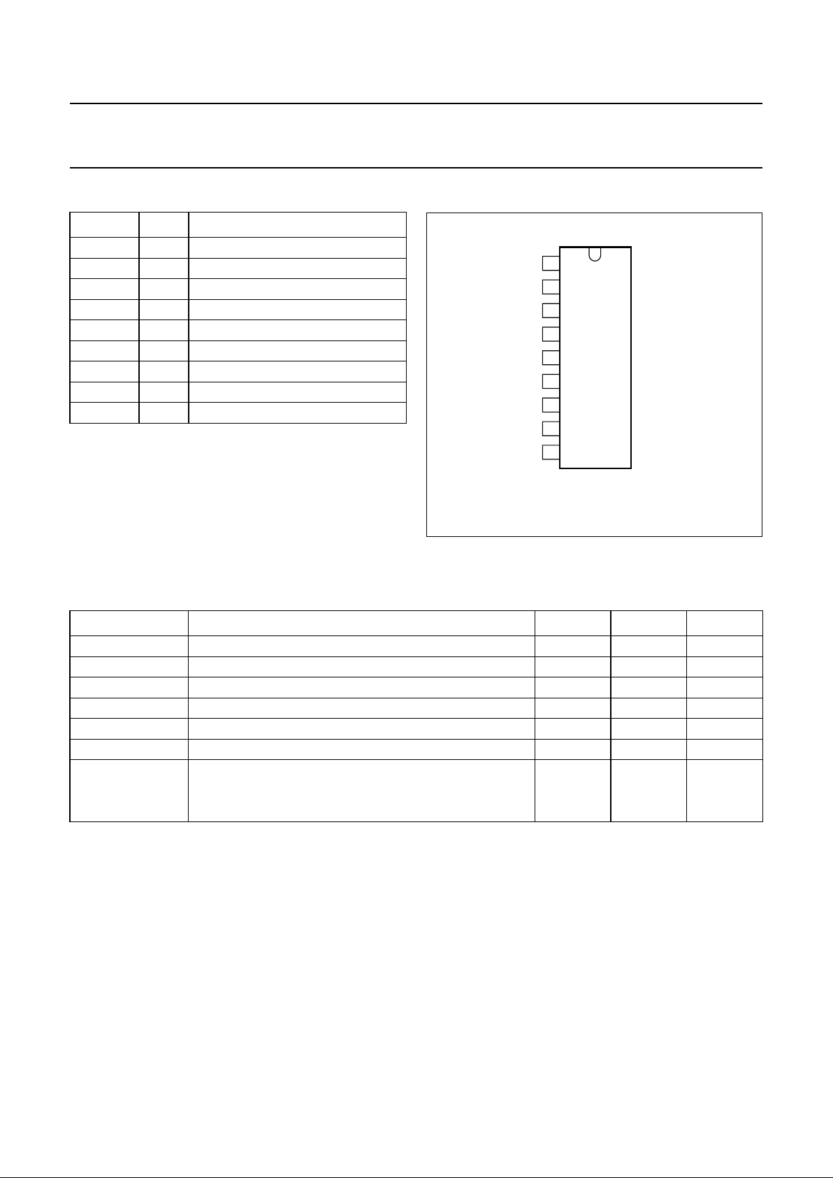
PINNING
SYMBOL PIN DESCRIPTION
V
i(1)
1 inverting input 1
V
i(2)
2 inverting input 2
V
i(3)
3 inverting input 3
GND 4 ground (fin)
I
om
5 black current measurement output
V
DD
6 supply voltage
V
oc(3)
7 cathode output 3
V
oc(2)
8 cathode output 2
V
oc(1)
9 cathode output 1
handbook, halfpage
V
i(1)
V
i(2)
V
i(3)
GND
I
om
V
DD
V
oc(3)
V
oc(2)
V
oc(1)
1
2
3
4
5
6
7
8
9
TDA6108JF
MGL319
Fig.2 Pin configuration.
LIMITING VALUES
In accordance with the Absolute Maximum Rating System (IEC 134); voltages measured with respect to pin 4 (ground);
currents as specified in Fig.1; unless otherwise specified.
HANDLING
Inputs and outputs are protected against electrostatic discharge in normal handling. However, to be totally safe, it is
desirable to take normal precautions appropriate to handling MOS devices (see
“Handling MOS Devices”
).
QUALITY SPECIFICATION
Quality specification
“SNW-FQ-611 part D”
is applicable.
SYMBOL PARAMETER MIN. MAX. UNIT
V
DD
supply voltage 0 250 V
V
i
input voltage 0 12 V
V
om
measurement output voltage 0 6V
V
oc
cathode output voltage 0 V
DD
V
T
stg
storage temperature −55 +150 °C
T
j
junction temperature −20 +150 °C
V
es
electrostatic handling
human body model (HBM) − 2000 V
machine model (MM) − 300 V
1999 Oct 29 4
Philips Semiconductors Product specification
Triple video output amplifier TDA6108JF
THERMAL CHARACTERISTICS
Note
1. An external heatsink is necessary.
SYMBOL PARAMETER CONDITIONS VALUE UNIT
R
th(j-a)
thermal resistance from junction to ambient 56 K/W
R
th(j-fin)
thermal resistance from junction to fin note 1 11 K/W
R
th(h-a)
thermal resistance from heatsink to ambient 10 K/W
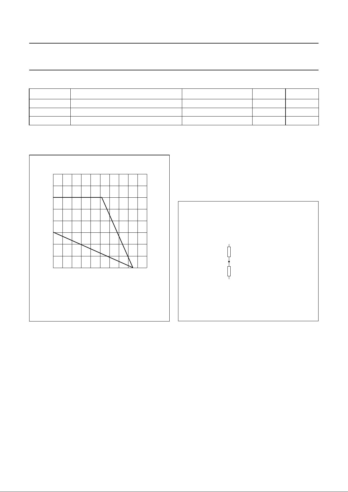
Thermal protection
The internal thermal protection circuit gives a decrease of
the slew rate at high temperatures: 10% decrease at
130 °C and 30% decrease at 145 °C (typical values on the
spot of the thermal protection circuit).
handbook, halfpage
−20 20
(1)
(2)
P
tot
(W)
180
T
amb
(°C)
8
6
2
0
4
60 100 140
MGL322
Fig.3 Power derating curves.
(1) Infinite heatsink.
(2) No heatsink.
handbook, halfpage
MGK279
5 K/W
outputs
fin
thermal protection circuit
6 K/W
Fig.4 Equivalent thermal resistance network.

1999 Oct 29 5
Philips Semiconductors Product specification
Triple video output amplifier TDA6108JF
CHARACTERISTICS
Operating range: Tj= −20 to +150 °C; VDD= 180 to 210 V. Test conditions: T
amb
=25°C; VDD= 200 V;
V
o(c1)=Vo(c2)=Vo(c3)
=1⁄2VDD; CL= 10 pF (CL consists of parasitic and cathode capacitance); R
th(h-a)
= 18 K/W
(measured in test circuit of Fig.8); unless otherwise specified.
SYMBOL PARAMETER CONDITIONS MIN. TYP. MAX. UNIT
I
q
quiescent supply current 8.8 10.3 11.7 mA
V
ref(int)
internal reference voltage
(input stage)
− 2.5 − V
R
i
input resistance − 3.2 − kΩ
G gain of amplifier 47.5 51.0 55.0
∆G gain difference −2.5 0 +2.5
V
O(c)
nominal output voltage at
pins 7, 8 and 9 (DC value)
Ii=0µA 116 129 142 V
∆V
O(c)(offset)
differential nominal output
offset voltage between
pins 7 and 8, 8 and 9 and
9 and 7 (DC value)
Ii=0µA − 05V
∆V
o(c)(T)
output voltage temperature
drift at pins 7, 8 and 9
−−10 − mV/K
∆V
o(c)(T)(offset)
differential output offset
voltage temperature drift
between pins 7 and 8,
8 and 9 and 7 and 9
− 0 − mV/K
I
o(m)(offset)
offsetcurrentofmeasurement
output (for 3 channels)
I
o(c)
=0µA;
1.5 V < Vi< 5.5 V;
3V<V
o(m)
<6V
−50 − +50 µA
∆I
o(m)
/∆I
o(c)
linearity of current transfer −100µA<I
o(c)
< 100 µA;
1.5 V < Vi< 5.5 V;
3V<V
o(m)
<6V
0.9 1.0 1.1
I
o(c)(max)
maximum peak output current
(pins 7, 8 and 9)
50V<V
o(c)<VDD
− 50 V − 28 − mA
V
o(c)(min)
minimum output voltage
(pins 7, 8 and 9)
Vi= 7.0 V; note 1 −−10 V
V
o(c)(max)
maximum output voltage
(pins 7, 8 and 9)
Vi= 1.0 V; note 1 VDD− 15 −−V
B
S
small signal bandwidth
(pins 7, 8 and 9)
V
o(c)
= 60 V (p-p) − 9.0 − MHz
B
L
large signal bandwidth
(pins 7, 8 and 9)
V
o(c)
= 100 V (p-p) − 8.0 − MHz
t
Pco
cathode output propagation
time 50% input to 50% output
(pins 7, 8 and 9)
V
o(c)
= 100 V (p-p)
square wave; f <1 MHz;
tr=tf=40ns
(pins 1, 2 and 3);
see Figs 6 and 7
− 32 − ns
 Loading...