

Philips tda6103q DATASHEETS

INTEGRATED CIRCUITS
DATA SH EET
TDA6103Q
Triple video output amplifier
Preliminary specification
File under Integrated Circuits, IC02
Philips Semiconductors
March 1995
Philips Semiconductors Preliminary specification
Triple video output amplifier TDA6103Q
FEATURES
• High bandwidth: 7.5 MHz typical; 60 V (peak-to-peak
value)
• High slew rate: 1600 V/µs
• Simple application with a variety of colour decoders
• Only one supply voltage needed
• Internal protection against positive appearing
Cathode-Ray Tube (CRT) flashover discharges
• One non-inverting input with a low minimum input
voltage of 1 V
• Thermal protection
• Controllable switch-off behaviour.
ORDERING INFORMATION
EXTENDED TYPE
NUMBER
PINS PIN POSITION MATERIAL CODE
TDA6103Q 9 DBS9 plastic SOT111BE
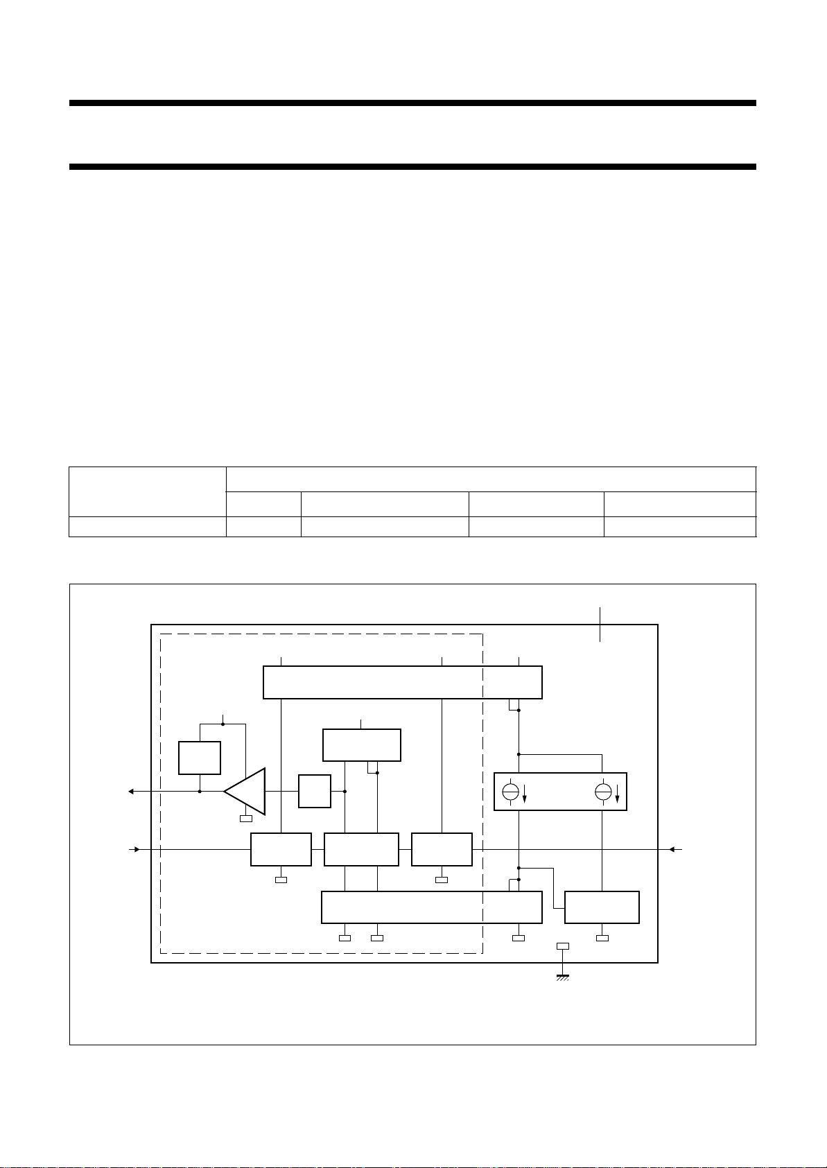
BLOCK DIAGRAM
GENERAL DESCRIPTION
The TDA6103Q includes three video output amplifiers in
one single in-line 9-pin medium power (SIL9MP) package
SOT111BE, using high-voltage DMOS technology,
intended to drive the three cathodes of a colour CRT.
PACKAGE
V
oc
(3x)
inverting
input
(3x)
9,8,7
1,2,3
3x
FLASH-
DIODE
V
DD
V
DD
MIRROR 2
V
DD
1x
LEVEL-
SHIFTER 1
V
bias
V
DD
MIRROR 3
DIFFERENTIAL
STAGE
V
DD
LEVEL-
SHIFTER 2
MIRROR 1
V
DD
CURRENT
SOURCES
4
6
TDA6103Q
THERMAL
PROTECTION
GND
MGA968
non-inverting
5
V
ip
input
March 1995 2
Fig.1 Block diagram (one amplifier shown).
Philips Semiconductors Preliminary specification
Triple video output amplifier TDA6103Q
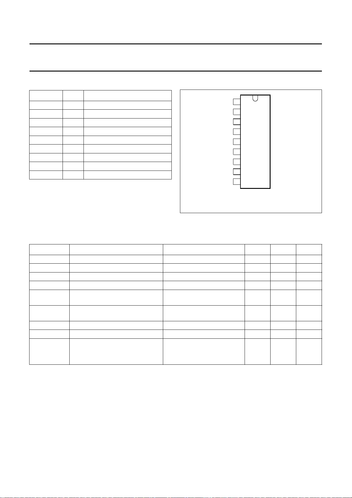
PINNING
SYMBOL PIN DESCRIPTION
1
V
V
V
GND
V
V
DD
V
oc3
V
oc2
V
oc1
i1
2
i2
3
i3
4
TDA6103Q
5
ip
6
7
8
9
MGA969
V
i1
V
i2
V
i3
1 inverting input 1
2 inverting input 2
3 inverting input 3
GND 4 ground, fin
V
ip
V
DD
V
oc3
V
oc2
V
oc1
5 non-inverting input
6 supply voltage
7 cathode output 3
8 cathode output 2
9 cathode output 1
Fig.2 Pin configuration.
LIMITING VALUES
In accordance with the Absolute Maximum Rating System (IEC 134). Voltages measured with respect to GND (pin 4);
currents as specified in Fig.1; unless otherwise specified.
SYMBOL PARAMETER CONDITIONS MIN. MAX. UNIT
V
DD
V
i
V
idm
V
oc
I
ocsmL
supply voltage 0 250 V
input voltage 0 12 V
differential mode input voltage −6+6V
cathode output voltage 0 V
LOW non-repetitive peak cathode
flashover discharge = 50 µC05A
DD
V
output current
I
ocsmH
HIGH non-repetitive peak cathode
flashover discharge = 100 nC 0 10 A
output current
T
stg
T
j
V
es
storage temperature −55 +150 °C
junction temperature −20 +150 °C
electrostatic handling
human body model (HBM) − tbf V
machine model (MM) − tbf V
HANDLING
Inputs and outputs are protected against electrostatic discharge in normal handling. However, to be totally safe, it is
desirable to take normal precautions appropriate to handling MOS devices (see
QUALITY SPECIFICATION
Quality specification
“SNW-FQ-611 part E”
number 9398 510 34011).
March 1995 3
is applicable and can be found in the
“Handling MOS Devices”
).
“Quality reference pocketbook”
(ordering
Philips Semiconductors Preliminary specification
Triple video output amplifier TDA6103Q
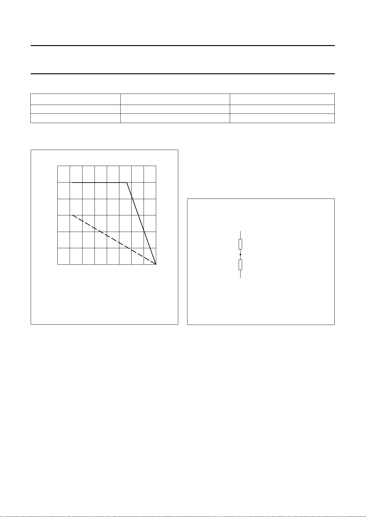
THERMAL RESISTANCE
SYMBOL PARAMETER THERMAL RESISTANCE
R
th j-fin
R
th h-a
Note
1. An external heatsink is necessary.
6
5
P
tot
(W)
4
3
from junction to fin; note 1 11 K/W
from heatsink to ambient 18 K/W
Thermal protection
MGA972
The internal thermal protection circuit gives a decrease of
the slew rate at high temperatures: 10% decrease at
130 °C and 30% decrease at 145 °C (typical values on the
spot of the thermal protection circuit).
(1)
2
1
0
(1) Infinite heatsink.
(2) No heatsink.
Fig.3 Power derating curves.
(2)
0 50 100–50
T ( C)
amb
150
o
OUTPUTS
5 K/W
Thermal protection circuit
6 K/W
FIN
MGA970
Fig.4 Equivalent thermal resistance network.
March 1995 4
 Loading...