

Philips tda6101q DATASHEETS

INTEGRATED CIRCUITS
DATA SH EET
TDA6101Q
Video output amplifier
Preliminary specification
Supersedes data of November 1991
File under Integrated Circuits, IC02
Philips Semiconductors
1995 Feb 07

Philips Semiconductors Preliminary specification
Video output amplifier TDA6101Q
FEATURES
• High bandwidth and high slew rate
• No external heatsink required
• Black-current measurement output for Automatic
Black-current Stabilization (ABS)
GENERAL DESCRIPTION
The TDA6101Q is a video output amplifier with 9 MHz
bandwidth. The device is contained in a single in-line 9-pin
medium power (DBS9MPF) package, using high-voltage
DMOS technology, intended to drive the cathode of a
colour CRT.
• Two cathode outputs; one for DC currents, and one for
transient currents
• A feedback output separated from the cathode outputs
• Internal protection against positive appearing
Cathode-Ray Tube (CRT) flashover discharges
• ESD protection
• Simple application with a variety of colour decoders
• Differential input with a designed maximum common
mode input capacitance of 3 pF, a maximum differential
mode input capacitance of 0.5 pF and a differential input
voltage temperature drift of 20 µV/K
• Defined switch-off behaviour.
QUICK REFERENCE DATA
SYMBOL PARAMETER CONDITIONS MIN. TYP. MAX. UNIT
V
V
I
DDH
I
DDL
V
V
T
T
DDH
DDL
I
oc
stg
amb
, V
fb
high level supply voltage 0 − 250 V
low level supply voltage 0 − 14 V
quiescent high voltage supply current Voc= 0.5V
quiescent low voltage supply current Voc= 0.5V
DDH
DDH
input voltage 0 − V
output voltage V
3.5 4.4 5.5 mA
2.2 2.8 3.5 mA
DDL
DDL
− V
DDH
storage temperature −55 − +150 °C
operating ambient temperature −20 − +65 °C
V
V
ORDERING INFORMATION
TYPE NUMBER
TDA6101Q DBS9MPF plastic DIL-bent-SIL medium power package with fin; 9 leads SOT111-1
1995 Feb 07 2
PACKAGE
NAME DESCRIPTION VERSION
Philips Semiconductors Preliminary specification
Video output amplifier TDA6101Q
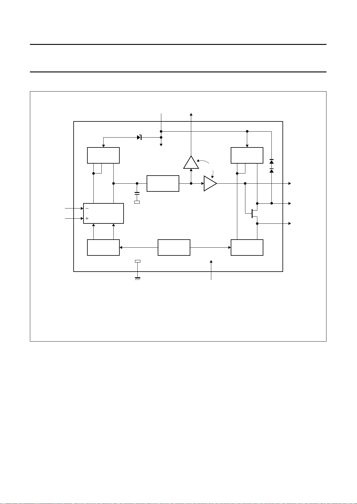
BLOCK DIAGRAM
handbook, full pagewidth
inverting
input
non-inverting
input
3
1
MIRROR
DIFFERENTIAL
STAGE
MIRROR
supply voltage
input HIGH
6
7 V
V
bias
C
par
feedback
output
9
MIRROR
FOLLOWERS
TDA6101Q
CURRENT
SOURCE
42
ground
(substrate)
supply voltage
input LOW
MIRROR
MCD356
7
8
5
cathode
transient
output
cathode
DC output
black current
measurement
output
1995 Feb 07 3
Fig.1 Block diagram.
Philips Semiconductors Preliminary specification
Video output amplifier TDA6101Q
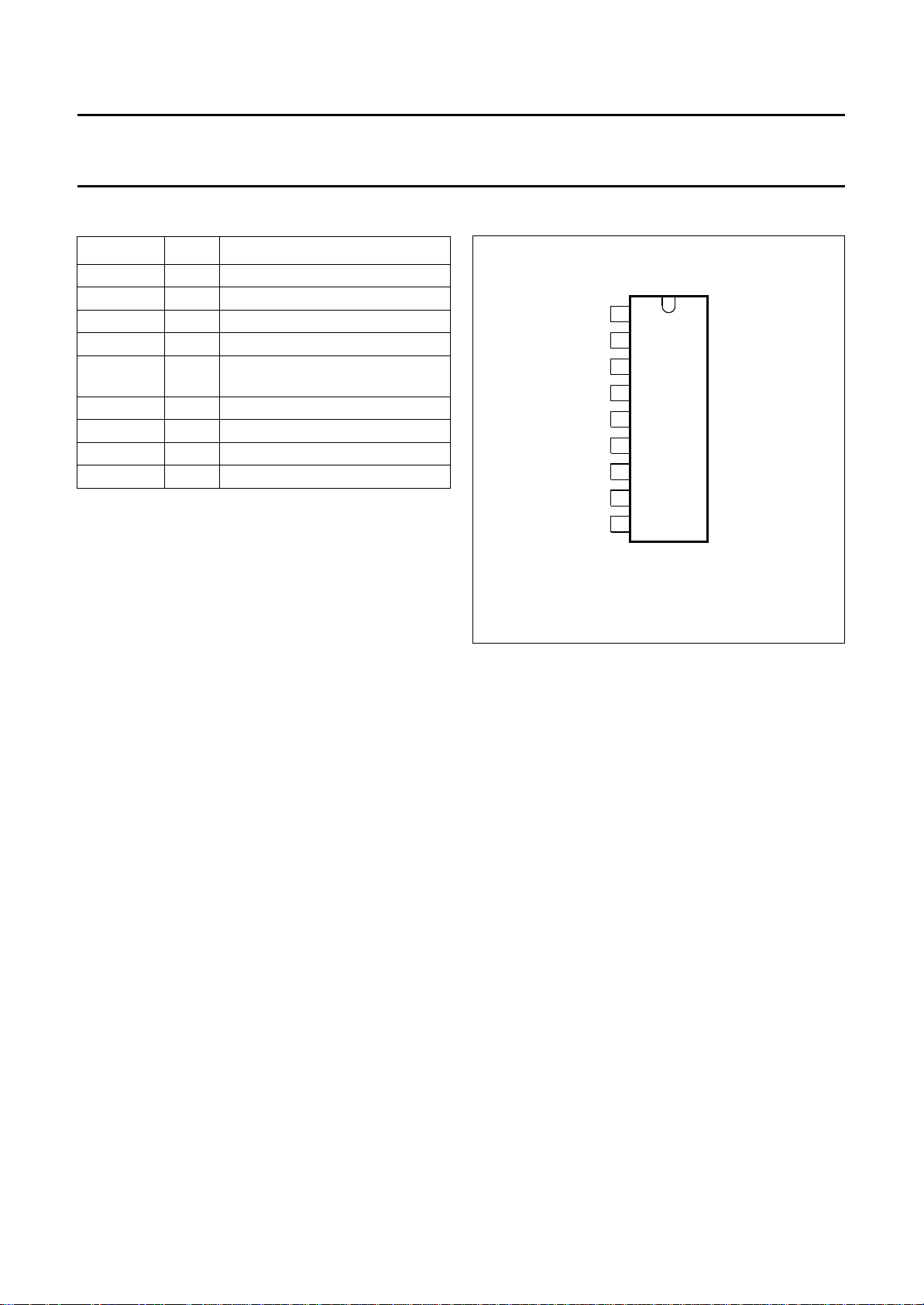
PINNING
SYMBOL PIN DESCRIPTION
V
ip
V
DDL
V
in
GND 4 ground, substrate
I
om
V
DDH
V
cn
V
oc
V
fb
1 non-inverting voltage input
2 supply voltage LOW
3 inverting voltage input
5 black current measurement
output
6 supply voltage HIGH
7 cathode transient voltage output
8 cathode DC voltage output
9 feedback voltage output
handbook, halfpage
V
V
V
DDL
V
GND
I
om
DDH
V
V
V
1
ip
2
3
in
4
TDA6101Q
5
6
7
cn
8
oc
9
fb
MCD355
Fig.2 Pin configuration.
1995 Feb 07 4
 Loading...