

Philips TDA5744TS, TDA5745TS Datasheet

INTEGRATED CIRCUITS
DATA SH EET
TDA5744; TDA5745
Low power mixers/oscillators for
hyperband tuners
Preliminary specification
File under Integrated Circuits, IC02
1998 Mar 09
Philips Semiconductors Preliminary specification
Low power mixers/oscillators for
hyperband tuners
FEATURES
• Mixers/oscillators for hyperband tuners
• Balanced mixer with a common emitter input for VHF
(single input)
• Balanced mixer with a common base input for UHF
(double input)
• 4-pin common emitter oscillator for VHF
• 4-pin common emitter oscillator for UHF
• Electronic band switch
• IF amplifier with a low output impedance to drive the
SAW filter directly (≈2kΩ load)
• Low power, low radiation and small size
• Pin compatible single-chip synthesizer mixer/oscillator
for Full Scale Tuners (FST) are available: TDA6404,
TDA6405 and TDA6405A.
QUICK REFERENCE DATA
TDA5744; TDA5745
APPLICATIONS
• Hyperband tuners for Europe using a 2-band
mixer/oscillator in a switched concept.
GENERAL DESCRIPTION
The TDA5744 and TDA5745 are 2-band mixers/oscillators
intended for VHF/UHF and hyperband tuners (see Fig.1).
The Integrated Circuits (ICs) include two double balanced
mixers and two oscillators, for the VHF and UHF band, and
an IF amplifier. With proper oscillator application and by
using a switchable inductor to split the VHF band into two
sub-bands (the full VHF/UHF and hyperband) the TV
bands can be covered. Two pins are available between
the mixer output and the IF amplifier input to enable IF
filtering for improved signal handling. Band selection is
made by band switch pin BS.
SYMBOL PARAMETER CONDITIONS MIN. TYP. MAX. UNIT
V
I
CC
T
T
f
i(RF)
CC
stg
amb
supply voltage operating 4.5 5 5.5 V
supply current − 58 − mA
IC storage temperature −40 − +150 °C
operating ambient temperature −20 − +85 °C
RF input frequency VHF band 45.25 − 399.25 MHz
UHF band 407.25 − 855.25 MHz
G
V
voltage gain VHF band − 27 − dB
UHF band − 38 − dB
F noise figure VHF band − 8 − dB
UHF band − 8.5 − dB
V
o
output voltage causing 1% cross
modulation in channel
VHF band − 119 − dBµV
UHF band − 118 − dBµV
ORDERING INFORMATION
TYPE
NUMBER
TDA5744TS;
TDA5745TS
NAME DESCRIPTION VERSION
SSOP24 plastic shrink small outline package; 24 leads; body width 5.3 mm SOT340-1
PACKAGE
1998 Mar 09 2

Philips Semiconductors Preliminary specification
Low power mixers/oscillators for
hyperband tuners
BLOCK DIAGRAM
handbook, full pagewidth
12 (13)
n.c.
11 (14)
n.c.
10 (15)
n.c.
8 (17)
n.c.
7 (18 )
n.c.
IFFIL2
IFFIL1
RFGND
VHFIN
6 (19)
5 (20)
4 (21)
3 (22)
VHF
STAGE
TDA5744
(TDA5745)
VHF
MIXER
DC
STABILIZER
IF
AMPLIFIER
VHF
OSCILLATOR
TDA5744; TDA5745
(12) 13
(11) 14
(10) 15
(9) 16
(4) 21
(3) 22
(2) 23
(1) 24
V
CC
IFOUT1
IFOUT2
GND
VHFOSCIB1
VHFOSCOC1
VHFOSCOC2
VHFOSCIB2
9 (16)
BS
UHFIN2
UHFIN1
The pin numbers in parenthesis represent the TDA5745.
2 (23)
1 (24)
ELECTRONIC
BAND
SWITCH
UHF
STAGE
UHF
MIXER
Fig.1 Block diagram.
UHF
OSCILLATOR
(8) 17
(7) 18
(6) 19
(5) 20
MGM466
UHFOSCIB1
UHFOSCOC1
UHFOSCOC2
UHFOSCIB2
1998 Mar 09 3
Philips Semiconductors Preliminary specification
Low power mixers/oscillators for
hyperband tuners
PINNING
SYMBOL
UHFIN1 1 24 UHF input 1
UHFIN2 2 23 UHF input 2
VHFIN 3 22 VHF input
RFGND 4 21 RF ground
IFFIL1 5 20 IF filter output 1
IFFIL2 6 19 IF filter output 2
n.c. 7 18 not connected
n.c. 8 17 not connected
BS 9 16 electronic band switch
n.c. 10 15 not connected
n.c. 11 14 not connected
n.c. 12 13 not connected
V
CC
IFOUT1 14 11 IF amplifier output 1
IFOUT2 15 10 IF amplifier output 2
GND 16 9 ground
UHFOSCIB1 17 8 UHF oscillator base input 1
UHFOSCOC1 18 7 UHF oscillator collector output 1
UHFOSCOC2 19 6 UHF oscillator collector output 2
UHFOSCIB2 20 5 UHF oscillator base input 2
VHFOSCIB1 21 4 VHF oscillator base input 1
VHFOSCOC1 22 3 VHF oscillator collector output 1
VHFOSCOC2 23 2 VHF oscillator collector output 2
VHFOSCIB2 24 1 VHF oscillator base input 2
TDA5744 TDA5745
PIN
DESCRIPTION
13 12 supply voltage
TDA5744; TDA5745
1998 Mar 09 4
Philips Semiconductors Preliminary specification
Low power mixers/oscillators for
hyperband tuners
handbook, halfpage
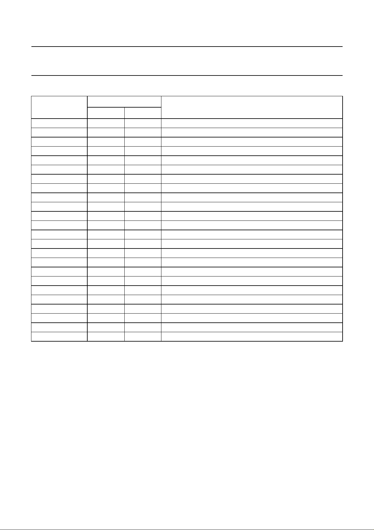
UHFIN1
UHFIN2
RFGND
VHFIN
IFFIL1
IFFIL2
n.c.
n.c.
BS
n.c.
n.c.
n.c.
1
2
3
4
5
6
TDA5744TS
7
8
9
10
11
MGM464
VHFOSCIB2
24
23
VHFOSCOC2
VHFOSCOC1
22
21
VHFOSCIB1
20
UHFOSCIB2
19
UHFOSCOC2
UHFOSCOC1
18
UHFOSCIB1
17
GND
16
IFOUT2
15
IFOUT1
14
V
1312
CC
handbook, halfpage
VHFOSCIB2
VHFOSCOC2
VHFOSCOC1
VHFOSCIB1
UHFOSCIB2
UHFOSCOC2
UHFOSCOC1
UHFOSCIB1
GND
IFOUT2
IFOUT1
V
CC
TDA5744; TDA5745
1
2
3
4
5
6
TDA5745TS
7
8
9
10
11
MGM465
24
23
22
21
20
19
18
17
16
15
14
1312
UHFIN1
UHFIN2
VHFIN
RFGND
IFFIL1
IFFIL2
n.c.
n.c.
BS
n.c.
n.c.
n.c.
Fig.2 Pin configuration for TDA5744TS.
Fig.3 Pin configuration for TDA5745TS.
1998 Mar 09 5
Philips Semiconductors Preliminary specification
Low power mixers/oscillators for
TDA5744; TDA5745
hyperband tuners
LIMITING VALUES
In accordance with the Absolute Maximum Rating System (IEC 134).
SYMBOL PARAMETER MIN. MAX. UNIT
I
O(n)
t
sc(max)
T
stg
T
amb
T
j
THERMAL CHARACTERISTICS
SYMBOL PARAMETER CONDITIONS VALUE UNIT
R
th(j-a)
CHARACTERISTICS
=5V; T
V
CC
output current of each pin to ground:
for TDA5744; pins 1 to 6, 9 and 13 to 24 −−10 mA
for TDA5745; pins 1 to 12, 16 and 19 to 24 −−10 mA
maximum short-circuit time (all pins to VCC and all pins to GND and RFGND) − 10 s
IC storage temperature −40 +150 °C
operating ambient temperature −20 +85 °C
junction temperature − 150 °C
thermal resistance from junction to ambient in free air 119 K/W
=25°C; unless otherwise specified; measured in Fig.11.
amb
SYMBOL PARAMETER CONDITIONS MIN. TYP. MAX. UNIT
Supplies
V
CC
I
CC
V
sw(VHF)
V
sw(UHF)
I
sw(VHF)
I
sw(UHF)
supply voltage 4.5 5 5.5 V
supply current − 58 65 mA
VHF band switching voltage 0 − 2V
UHF band switching voltage 3 − V
CC
V
VHF band switching current −−2µA
UHF band switching current V
sw(UHF)
=5V − 4.5 10 µA
IF amplifier
S
22
output reflection coefficient magnitude −−12.5 − dB
phase − 1.4 − deg
R
s
L
s
real part of Zo=Rs+jωL
imaginary part of
Zo=Rs+jωL
s
s
− 81 −Ω
− 9.5 − nH
VHF mixer (including IF amplifier)
f
i(RF)
F noise figure f
g
os
RF input frequency picture carrier frequency 45.25 − 399.25 MHz
= 50 MHz; see Figs 8 and 9 − 79dB
RF
f
= 150 MHz; see Figs 8 and 9 − 810dB
RF
f
= 300 MHz − 911dB
RF
optimum source
conductance for noise figure
fRF=50MHz − 0.7 − mS
f
= 150 MHz − 0.9 − mS
RF
f
= 300 MHz − 1.5 − mS
RF
1998 Mar 09 6
 Loading...