

Philips TDA5737M-C4, TDA5737M-C1-M1, TDA5737M-C1, TDA5736T-C2, TDA5736T-C1-M1 Datasheet
...
DATA SH EET
Product specification
Supersedes data of 1996 Oct 25
File under Integrated Circuits, IC02
1997 Feb 24
INTEGRATED CIRCUITS
TDA5736; TDA5737
5 V VHF, hyperband and UHF
mixers/oscillators
for TV and VCR 3-band tuners

1997 Feb 24 2
Philips Semiconductors Product specification
5 V VHF, hyperband and UHF mixers/oscillators
for TV and VCR 3-band tuners
TDA5736; TDA5737
FEATURES
• Balanced mixer with a common emitter input for band A
(single input)
• 2-pin oscillator for band A
• Balanced mixer with a common base input for bands B
and C (balanced input)
• 3-pin oscillator for band B
• 4-pin oscillator for band C
• Local oscillator buffer output for external prescaler
• SAW filter preamplifier with a low output impedance to
drive the SAW filter directly
• Band gap voltage stabilizer for oscillator stability
• Electronic band switch
• External IF filter between the mixer output and the IF
amplifier input.
APPLICATIONS
• 3-band all channel TV and VCR tuners
• Any standard.
GENERAL DESCRIPTION
The TDA5736 and TDA5737 are monolithic integrated
circuits that perform the mixer/oscillator functions for
bands A, B and C in TV and VCR tuners. These low power
mixer/oscillators require a power supply of 5 V and are
available in a very small package.
These devices give the designer the capability to design
an economical and physically small 3-band tuner.
They are suitable for European standards, as illustrated in
Fig.17, with the following RF bands: 48.25 to 168.25 MHz,
175.25 to 447.25 MHz and 455.25 to 855.25 MHz. With
an appropriate tuned circuit, they are also suitable for
NTSC all channel tuners (USA and Japan).
The tuner development time can be drastically reduced by
using these devices.
QUICK REFERENCE DATA
Note
1. The limits are related to the tank circuits used in Fig.17 and the intermediate frequency. Frequency bands may be
adjusted by the choice of external components.
SYMBOL PARAMETER CONDITIONS MIN. TYP. MAX. UNIT
V
P
supply voltage − 5.0 − V
I
P
supply current − 50 − mA
f
RF
frequency range RF input; band A; note 1 41 − 171 MHz
RF input; band B; note 1 166 − 451 MHz
RF input; band C; note 1 446 − 861 MHz
G
v
voltage gain band A − 23 − dB
band B − 34 − dB
band C − 34 − dB
NF noise figure band A − 7.5 − dB
band B − 8 − dB
band C − 9 − dB
V
o
output voltage level causing 1% cross
modulation in channel
band A − 116 − dBµV
band B − 115 − dBµV
band C − 115 − dBµV
1997 Feb 24 3
Philips Semiconductors Product specification
5 V VHF, hyperband and UHF mixers/oscillators
for TV and VCR 3-band tuners
TDA5736; TDA5737
ORDERING INFORMATION
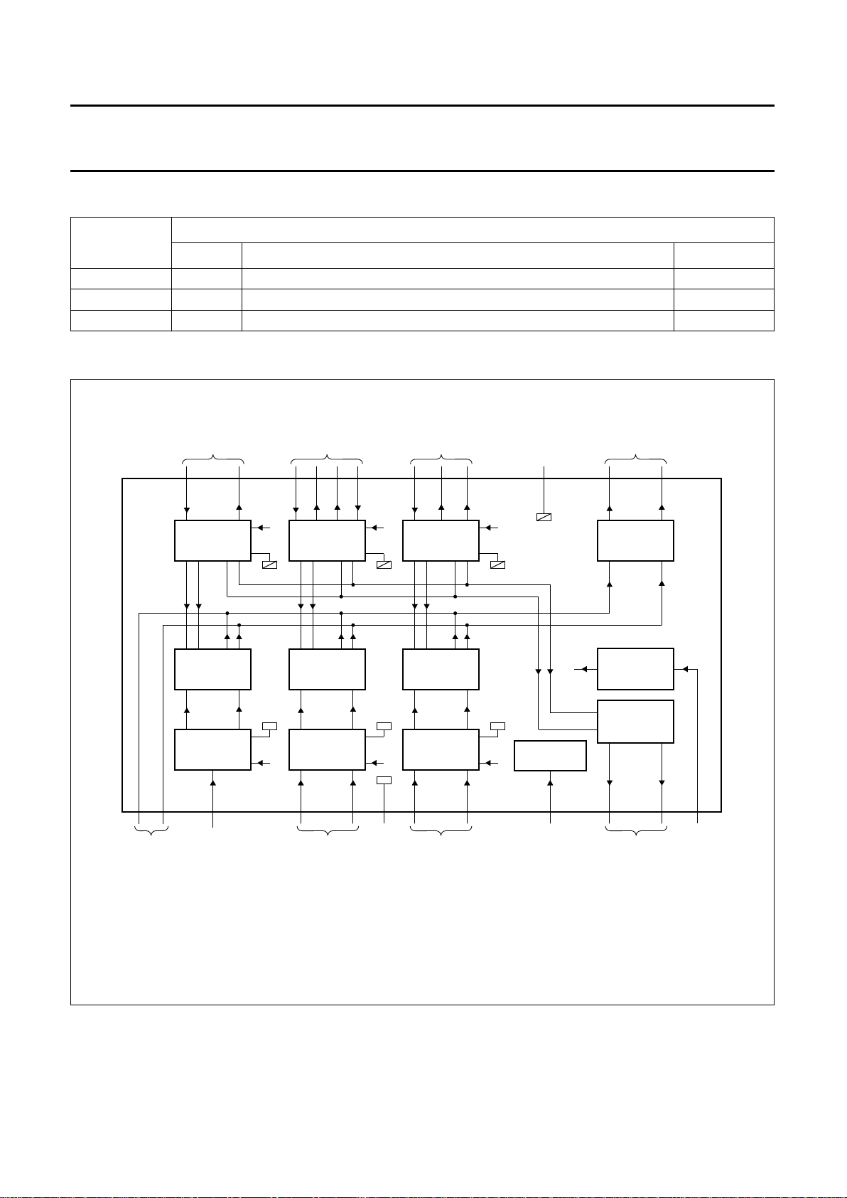
BLOCK DIAGRAM
TYPE
NUMBER
PACKAGE
NAME DESCRIPTION VERSION
TDA5736T SO24 plastic small outline package; 24 leads; body width 7.5 mm SOT137-1
TDA5736M SSOP24 plastic shrink small outline package; 24 leads; body width 5.3 mm SOT340-1
TDA5737M SSOP24 plastic shrink small outline package; 24 leads; body width 5.3 mm SOT340-1
handbook, full pagewidth
MGE971
BAND A
OSCILLATOR
BAND C
OSCILLATOR
BAND B
OSCILLATOR
MIXER MIXER MIXER
BAND B
STAGE
BAND C
STAGE
BAND A
STAGE
DC
STABILIZER
LOCAL
OSCILLATOR
AMPLIFIER
ELECTRONIC
BAND
SWITCH
IF
AMPLIFIER
band switch
input
TDA5736T
TDA5736M
TDA5737M
RF
GND
band A
input
band B
inputs
V
P
band C
inputs
IF
filter input
band C oscillator
tuned cicuit
band B oscillator
tuned cicuit
IF outputs
local oscillator
amplifier outputs
band A oscillator
tuned cicuit
GND
(24)1(23)
2
(19)
6
(21)
4
(20)5(22)3(18)
7
(17)
8
(16)
9
(15)
10
(14)11(13)
12
15
(10)
14
(11)
13
(12)
21
(4)
23
(2)
19
(6)
17
(8)
16
(9)
22
(3)
24
(1)
20
(5)
18
(7)
Fig.1 Block diagram.
The numbers in parenthesis represent the TDA5737M.

1997 Feb 24 4
Philips Semiconductors Product specification
5 V VHF, hyperband and UHF mixers/oscillators
for TV and VCR 3-band tuners
TDA5736; TDA5737
PINNING
SYMBOL
PIN
DESCRIPTION
TDA5736 TDA5737
IFIN1 1 24 IF filter input 1
IFIN2 2 23 IF filter input 2
RFGND 3 22 ground for RF inputs
CIN1 4 21 band C input 1
CIN2 5 20 band C input 2
AIN 6 19 band A input
BIN1 7 18 band B input 1
BIN2 8 17 band B input 2
V
P
9 16 supply voltage
LOOUT1 10 15 local oscillator amplifier output 1
LOOUT2 11 14 local oscillator amplifier output 2
BS 12 13 band switch input
IFOUT1 13 12 IF amplifier output 1
IFOUT2 14 11 IF amplifier output 2
GND 15 10 ground (0 V)
BOSCOC1 16 9 band B oscillator output collector 1
BOSCOC2 17 8 band B oscillator output collector 2
COSCIB1 18 7 band C oscillator input base 1
BOSCIB 19 6 band B oscillator input base
COSCOC1 20 5 band C oscillator output collector 1
AOSCOC 21 4 band A oscillator output collector
COSCOC2 22 3 band C oscillator output collector 2
AOSCIB 23 2 band A oscillator input base
COSCIB2 24 1 band C oscillator input base 2
1997 Feb 24 5
Philips Semiconductors Product specification
5 V VHF, hyperband and UHF mixers/oscillators
for TV and VCR 3-band tuners
TDA5736; TDA5737
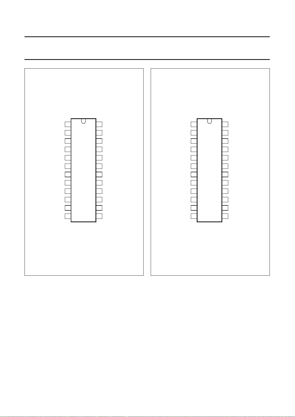
Fig.2 Pin configuration (TDA5736M, TDA5736T).
handbook, halfpage
TDA5736M
TDA5736T
MBE383
1
2
3
4
5
6
7
8
9
10
11
12
24
23
22
21
20
19
18
17
16
15
14
13
IFIN2
RFGND
CIN1
CIN2
AIN
BIN1
BIN2
LOOUT1
LOOUT2
BS
V
P
IFIN1 COSCIB2
COSCIB1
BOSCOC2
BOSCOC1
GND
IFOUT2
IFOUT1
COSCOC2
AOSCIB
BOSCIB
COSCOC1
AOSCOC
Fig.3 Pin configuration (TDA5737M).
handbook, halfpage
TDA5737M
MGE970
1
2
3
4
5
6
7
8
9
10
11
12
24
23
22
21
20
19
18
17
16
15
14
13
IFIN2
RFGND
CIN1
CIN2
AIN
BIN1
BIN2
LOOUT1
LOOUT2
BS
V
P
IFIN1COSCIB2
COSCIB1
BOSCOC2
BOSCOC1
GND
IFOUT2
IFOUT1
COSCOC2
AOSCIB
BOSCIB
COSCOC1
AOSCOC
1997 Feb 24 6
Philips Semiconductors Product specification
5 V VHF, hyperband and UHF mixers/oscillators
for TV and VCR 3-band tuners
TDA5736; TDA5737
LIMITING VALUES
In accordance with the Absolute Maximum Rating System (IEC 134).
HANDLING
Human Body Model:
• For TDA5736 GND (15), RFGND (3), V
P
(9) separate
• For TDA5737 GND (10), RFGND (22), VP(16) separate.
All pins withstand 2000 V in accordance with the
“UZW-BO/FQ-A302”
. Philips specification equivalent to the
“MIL-STD-883C”
category B (2000 V) except pins 16 and 17 (8 and 9 for the TDA5737) which withstand 1000 V;
R = 1500 Ω, C = 100 pF.
Machine Model:
• For TDA5736 GND (15), RFGND (3), VP(9) separate
• For TDA5737 GND (10), RFGND (22), VP(16) separate.
All pins withstand 200 V in accordance with the
“UZW-BO/FQ-B302”
, Philips specification (revision of: Nov. 6th, 1990)
except pins 16 and 17 (8 and 9 for the TDA5737) which withstand 100 V; R = 0 Ω, C = 200 pF.
THERMAL CHARACTERISTICS
SYMBOL PARAMETER MIN. MAX. UNIT
V
P
supply voltage −0.3 +7.0 V
V
SW
switching voltage −0.3 +7.0 V
V
n(max)
maximum voltage on each pin with a 22 kΩ resistor connected in series − 35 V
I
O
output current of each pin to ground −−10 mA
t
sc(max)
maximum short-circuit time (all pins) − 10 s
T
stg
IC storage temperature −55 +150 °C
T
amb
operating ambient temperature −20 +80 °C
T
j
junction temperature − 150 °C
SYMBOL PARAMETER VALUE UNIT
R
th j-a
thermal resistance from junction to ambient in free air
SSOP24 120 K/W
SO24 75 K/W
1997 Feb 24 7
Philips Semiconductors Product specification
5 V VHF, hyperband and UHF mixers/oscillators
for TV and VCR 3-band tuners
TDA5736; TDA5737
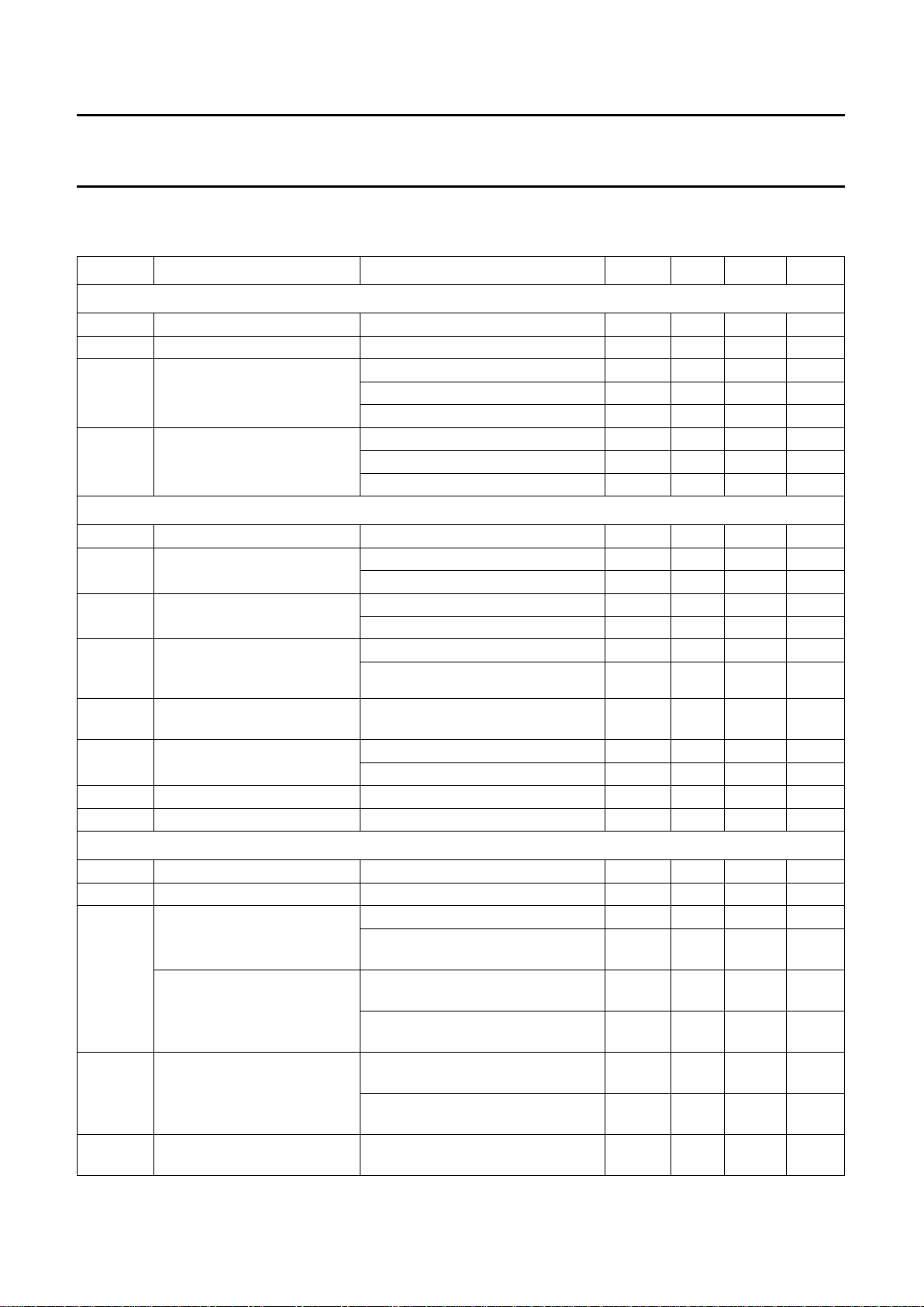
CHARACTERISTICS
V
P
=5V; T
amb
=25°C; measured in circuit of Fig.17; unless otherwise specified.
SYMBOL PARAMETER CONDITIONS MIN. TYP. MAX. UNIT
Supply
V
P
supply voltage 4.5 5.0 5.5 V
I
P
supply current 42 50 58 mA
V
SW
switching voltage depending
on supply voltage V
P
band A; note 1 0 − 0.18VPV
band B; note 1 0.26V
P
− 0.47VPV
band C; note 1 0.55V
P
− V
P
V
I
SW
switching current band A; note 1 −−2µA
band B; note 1 −−10 µA
band C; note 1 −−25 µA
Band A mixer (including IF amplifier)
f
RF
frequency range note 2 41 − 171 MHz
G
v
voltage gain fRF= 50 MHz; see Fig.4; note 3 20.5 23.0 25.5 dB
f
RF
= 170 MHz; see Fig.4; note 3 20.5 23.0 25.5 dB
NF noise figure f
RF
= 50 MHz; see Figs.5 and 6 − 7.5 9 dB
f
RF
= 170 MHz; see Figs.5 and 6 − 910dB
V
o
output voltage level causing
1% cross modulation in
channel
fRF= 50 MHz; see Fig.7 115 118 − dBµV
f
RF
= 170 MHz; see Fig.7 113 116 − dBµV
V
i
input voltage level causing
10 kHz pulling in channel
fRF= 170 MHz; note 4 96 100 − dBmV
g
os
optimum source conductance
for noise figure
fRF=50MHz − 0.5 − mS
f
RF
= 170 MHz − 1.1 − mS
Y
i
input admittance fRF= 50 to 170 MHz; see Fig.12 − 0.3 − mS
C
i
input capacitance fRF= 50 to 170 MHz; see Fig.12 − 1.9 − pF
Band A oscillator
f
osc
frequency range 0.45 V < Vt< 28 V; notes 1 and 5 80 − 210 MHz
f
shift
frequency shift ∆Vp= 5%; note 6 −−53 kHz
f
drift
frequency drift with no
compensation
∆T=25°C; NP0 capacitors; note7 −−650 kHz
5 s to 15 mins after switch on; NP0
capacitors; note 8
−−250 kHz
frequency drift with
compensation
∆T=25°C; notes7 and 9;
see Fig.18
−−500 kHz
5 s to 15 mins after switch on;
notes 8 and 9; see Fig.18
−−100 kHz
V
ripple
ripple susceptibility of supply
voltage (peak-to-peak value)
f
osc
= 80 MHz;
4.75 V < VP< 5.25 V; see Fig.8
20 −− mV
f
osc
= 210 MHz;
4.75 V < VP< 5.25 V; see Fig.8
20 −− mV
Φ
N
phase noise measured at the IF output at 10 kHz
offset; Vo= 105 dBµV
81 −− dBc/Hz
1997 Feb 24 8
Philips Semiconductors Product specification
5 V VHF, hyperband and UHF mixers/oscillators
for TV and VCR 3-band tuners
TDA5736; TDA5737
Band B mixer (including IF amplifier)
f
RF
frequency range note 2 166 − 451 MHz
G
v
voltage gain fRF= 170 MHz; see Fig.9; note 3 31 34 37 dB
f
RF
= 450 MHz; see Fig.9; note 3 31 34 37 dB
N noise figure
(not corrected for image)
f
RF
= 170 MHz; see Fig.10 − 810dB
f
RF
= 450 MHz; see Fig.10 − 810dB
V
o
output voltage level causing
1% cross modulation in
channel
fRF= 170 MHz; see Fig.7 114 117 − dBµV
f
RF
= 450 MHz; see Fig.7 112 115 − dBµV
V
i
input voltage level causing
10 kHz pulling in channel
fRF= 450 MHz; note 4 83 87 − dBµV
Z
i
input impedance (Rs+jLsω)fRF= 170 to 450 MHz; see Fig.13 − 23 −Ω
f
RF
= 170 to 450 MHz; see Fig.13 − 9 − nH
Band B oscillator
f
osc
frequency range 0.45 V < Vt< 28 V; notes 1 and 5 205 − 490 MHz
f
shift
frequency shift ∆Vp= 5%; note 6 −−53 kHz
f
drift
frequency drift with no
compensation
∆T=25°C; NP0 capacitors; note7 −−2000 kHz
5 s to 15 mins after switch on; NP0
capacitors; note 8
−−750 kHz
frequency drift with
compensation
∆T=25°C; notes7 and 9;
see Fig.18
−−750 kHz
5 s to 15 mins after switch on;
notes 8 and 9; see Fig.18
−−300 kHz
V
ripple
ripple susceptibility of supply
voltage (peak-to-peak value)
f
osc
= 250 MHz;
4.75 V < VP< 5.25 V; see Fig.8
20 −− mV
f
osc
= 490 MHz;
4.75 V < VP< 5.25 V; see Fig.8
20 −− mV
Φ
N
phase noise measured at the IF output at 10 kHz
offset; Vo= 105 dBmV
81 −− dBc/Hz
Band C Mixer (including IF amplifier)
f
RF
frequency range note 2 446 − 861 MHz
G
v
voltage gain fRF= 450 MHz; see Fig.9; note 3 31 34 37 dB
f
RF
= 860 MHz; see Fig.9; note 3 31 34 37 dB
N noise figure
(not corrected for image)
f
RF
= 450 MHz; see Fig.10 − 911dB
f
RF
= 860 MHz; see Fig.10 − 911dB
V
o
output voltage level causing
1% cross modulation in
channel
fRF= 450 MHz; see Fig.7 112 115 − dBµV
f
RF
= 860 MHz; see Fig.7 112 115 − dBµV
V
i
input voltage level causing
10 kHz pulling in channel
fRF= 860 MHz; note 4 91 95 − dBµV
Z
I
input impedance (Rs+jLsω)fRF= 450 to 860 MHz; see Fig.14 − 28 −Ω
f
RF
= 450 to 860 MHz; see Fig.14 − 10 − nH
SYMBOL PARAMETER CONDITIONS MIN. TYP. MAX. UNIT

1997 Feb 24 9
Philips Semiconductors Product specification
5 V VHF, hyperband and UHF mixers/oscillators
for TV and VCR 3-band tuners
TDA5736; TDA5737
Notes
1. −20 °C<T
amb
< +80 °C; 4.5 V < VP< 5.5 V.
2. The RF frequency range is defined by the oscillator frequency range and the intermediate frequency.
3. The gain is defined as the transducer gain (measured in Fig.17) plus the voltage transformation ratio of L7 to L8
(10 : 2, 15.4 dB including transformer loss).
4. The input level causing 10 kHz frequency detuning at the LO output. f
osc=fRF
+ 33.4 MHz.
5. Limits are related to the tank circuits used in Fig.17. Frequency bands may be adjusted by the choice of external
components.
6. The frequency shift is defined as the change in oscillator frequency when the supply voltage varies from
VP= 5 to 4.75 V and from VP= 5 to 5.25 V.
Band C oscillator
f
osc
frequency range 0.45 V < Vt< 28 V; notes 1 and 5 485 − 900 MHz
f
shift
frequency shift ∆VP= 5%; note 6 −−53 kHz
f
drift
frequency drift with no
compensation
∆T=25°C; NP0 capacitors; note7 −−2800 kHz
5 s to 15 mins after switch on; NP0
capacitors; note 8
−−700 kHz
frequency drift with
compensation
∆T=25°C; notes7 and 9;
see Fig.18
−−1000 kHz
5 s to 15 mins after switch on;
notes 8 and 9; see Fig.18
−−250 kHz
V
ripple
ripple susceptibility of supply
voltage (peak to peak value)
f
osc
= 485 MHz;
4.75 V < VP< 5.25 V; see Fig.8
20 −− mV
f
osc
= 900 MHz;
4.75 V < VP< 5.25 V; see Fig.8
18 −− mV
Φ
N
phase noise measured at the IF output at 10 kHz
offset; Vo= 105 dBµV
81 −− dBc/Hz
LO output
Z
O
output admittance (YP+jωCP)YP= 80 MHz; see Fig.12 − 2.5 − mS
Y
P
= 900 MHz; see Fig.12 − 5 − mS
C
P
; see Fig.12 − 0.9 − pF
V
o
output voltage RL=50Ω; 0<Vt< 35 V 80 91 100 dBµV
SRF spurious signal on LO output
with respect to LO output
signal
R
L
=50Ω; 0.2V<Vt<35V;
notes 1 and 10
−−−10 dB
HLO LO signal harmonics with
respect to LO signal
R
L
=50Ω; 0<Vt< 35 V; note 1 −−−10 dB
IF amplifier
S
22
output reflection coefficient magnitude; see Fig.15 −−16 − dB
phase; see Fig.15 − 12 − deg.
Z
O
output impedance (Rs+jLsω)R
s
− 67 −Ω
L
s
− 20 − nH
SYMBOL PARAMETER CONDITIONS MIN. TYP. MAX. UNIT
 Loading...