

Philips tda5731m DATASHEETS

INTEGRATED CIRCUITS
DATA SH EET
TDA5731M
Low power VHF, UHF and
hyperband mixer/oscillator for TV
and VCR 3-band tuners
Product specification
File under Integrated Circuits, IC02
Philips Semiconductors
1995 Mar 21
Philips Semiconductors Product specification
Low power VHF, UHF and hyperband
mixer/oscillator for TV and VCR 3-band tuners
FEATURES
• Balanced mixer with a common emitter input for band A
(single input)
• 2-pin oscillator for bands A and B
• 3-pin oscillator for band C
• Balanced mixer with a common base input for band B
and C (balanced input)
• Local oscillator buffer output for external synthesizer
• SAW filter preamplifier with a low output impedance to
drive the SAW filter directly
• Electronic band switch.
APPLICATIONS
• 3-band TV tuners
• 3-band TV front-ends
• 3-band VCR tuners
• 3-band VCR front-ends.
GENERAL DESCRIPTION
The TDA5731M is a monolithic integrated circuit that
performs the band A, band B and band C mixer/oscillator
functions in TV and VCR tuners. This low power
mixer/oscillator circuit requires a power supply of 5 V and
is available in a very small package outline. This device
gives the designer the capability to design an economical
and physically small 3-band tuner. The tuner development
time can be drastically reduced by using this device.
In addition, when hyperband is not required, the
TDA5731M may be used in a VHF/UHF tuner with an
appropriate tuned circuit for VHFl and VHFlll in band A and
the tuned circuit of band C for UHF.
TDA5731M
QUICK REFERENCE DATA
SYMBOL PARAMETER CONDITIONS MIN. TYP. MAX. UNIT
V
P
I
P
f
R
N noise figure band A − 7.5 − dB
IP intermodulation band A −−66 − dB
G
v
ORDERING INFORMATION
TYPE
NUMBER
TDA5731M SSOP20 plastic shrink small outline package; 20 leads; body width 4.4 mm SOT266-1
supply voltage − 5.0 − V
supply current − 36 − mA
frequency range band A 42 − 180 MHz
band B 160 − 470 MHz
band C 430 − 860 MHz
band B − 8.0 − dB
band C − 9.0 − dB
band B −−66 − dB
band C −−66 − dB
voltage gain band A − 23 − dB
band B − 34 − dB
band C − 33 − dB
PACKAGE
NAME DESCRIPTION VERSION
1995 Mar 21 2
Philips Semiconductors Product specification
Low power VHF, UHF and hyperband
mixer/oscillator for TV and VCR 3-band tuners
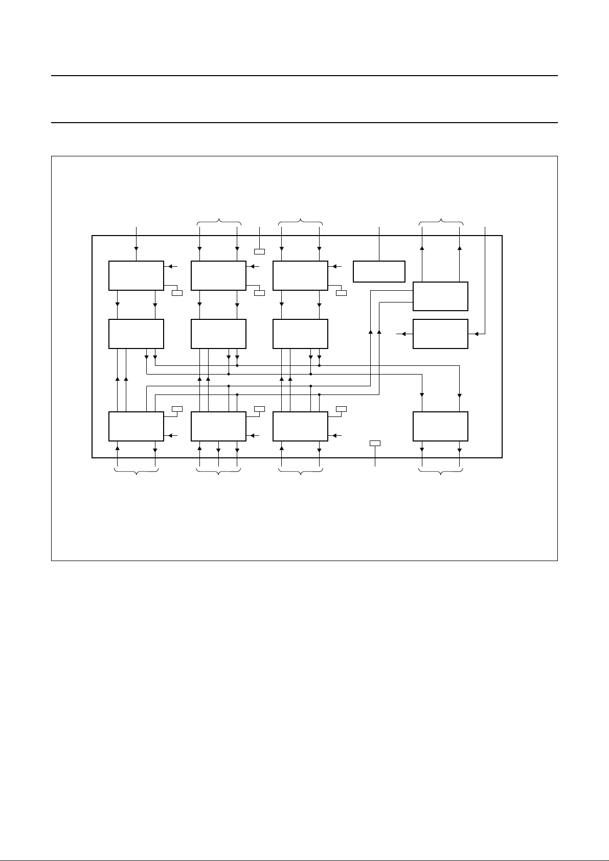
BLOCK DIAGRAM
handbook, full pagewidth
band C
band A
input
15 20 19 18 17 16 14 13 12 11
BAND A
STAGE
MIXER MIXER MIXER
inputs
BAND C
STAGE
RF
GND
band B
inputs
BAND B
STAGE
V
P
DC
STABILIZER
local oscillator
amplifier outputs
LOCAL
OSCILLATOR
AMPLIFIER
ELECTRONIC
BAND
SWITCH
TDA5731M
band switch
input
BAND A
OSCILLATOR
13
band A oscillator
tuned cicuit
BAND C
OSCILLATOR
26
band C oscillator
tuned cicuit
BAND B
OSCILLATOR
574
band B oscillator
tuned cicuit
Fig.1 Block diagram.
TDA5731M
8
GND
IF
AMPLIFIER
910
IF outputs
MBE374
1995 Mar 21 3

Philips Semiconductors Product specification
Low power VHF, UHF and hyperband
mixer/oscillator for TV and VCR 3-band tuners
PINNING
SYMBOL PIN DESCRIPTION
AOSCIB 1 band A oscillator input base
COSCIB 2 band C oscillator input base
AOSCOC 3 band A oscillator output collector
COSCOC1 4 band C oscillator output
collector 1
BOSCIB 5 band B oscillator input base
COSCOC2 6 band C oscillator output
collector 2
BOSCOC 7 band B oscillator output collector
GND 8 ground (0 V)
IFOUT1 9 IF amplifier output 1
IFOUT2 10 IF amplifier output 2
BS 11 band switch input
LOOUT1 12 local oscillator amplifier output 1
LOOUT2 13 local oscillator amplifier output 2
V
P
14 supply voltage
AIN 15 band A input
BIN1 16 band B input 1
BIN2 17 band B input 2
RFGND 18 ground for RF input
CIN1 19 band C input 1
CIN2 20 band C input 2
handbook, halfpage
1
COSCIB
AOSCOC
COSCOC1
BOSCIB
COSCOC2
BOSCOC
IFOUT1
IFOUT2
GND
2
3
4
5
TDA5731M
6
7
8
9
10
Fig.2 Pin configuration.
MBE373
TDA5731M
20
CIN2AOSCIB
CIN1
19
RFGND
18
17
BIN2
16
BIN1
15
AIN
V
14
P
13
LOOUT2
12
LOOUT1
BS
11
1995 Mar 21 4
Philips Semiconductors Product specification
Low power VHF, UHF and hyperband
TDA5731M
mixer/oscillator for TV and VCR 3-band tuners
LIMITING VALUES
In accordance with the Absolute Maximum Rating System (IEC 134).
SYMBOL PARAMETER MIN. MAX/ UNIT
V
P
V
SW(max)
V
P(op)
V
n(max)
I
O
t
sc(max)
T
stg
T
amb
T
j
THERMAL CHARACTERISTICS
SYMBOL PARAMETER VALUE UNIT
R
th j-a
supply voltage −0.3 +7.0 V
maximum switching voltage −0.3 +7.5 V
operating supply voltage 4.5 5.5 V
maximum voltage on each pin with a 22 kΩ resistor
− 35 V
connected in series
output current of each pin to ground −−10 mA
maximum short-circuit time (all pins) − 10 s
storage temperature −55 +150 °C
operating ambient temperature −10 +80 °C
junction temperature − +150 °C
thermal resistance from junction to ambient in free air 120 K/W
HANDLING
Human Body Model: GND (8), RFGND (18), V
(14) shorted together. Pins 4, 6 and 7 withstand 500 V. All other pins
P
withstand 2000 V.
Machine Model: GND (8), RFGND (18), VP(14) shorted together. Pins 4, 6 and 7 withstand 50 V. All other pins
withstand 200 V.
IF AMPLIFIER CHARACTERISTICS
=5V; T
V
P
=25°C; differentialy measured at 36 MHz; measured in circuit of Fig.6; unless otherwise specified.
amb
TYP.
SYMBOL PARAMETER CONDITIONS MIN.
MAX. UNIT
MOD. PHASE
S
22
Z
o
output reflection coefficient note 1; see Fig.11 −−14 +9 − dB/°
output impedance (Rs+Ls)R
s
L
s
− 74 −Ω
− 21 − nH
Note
1. All S parameters are referenced to a 50 Ω system.
1995 Mar 21 5
Philips Semiconductors Product specification
Low power VHF, UHF and hyperband
TDA5731M
mixer/oscillator for TV and VCR 3-band tuners
CHARACTERISTICS
V
=5V; T
P
SYMBOL PARAMETER CONDITIONS MIN. TYP. MAX. UNIT
Supply (T
V
P
I
P
V
SW
I
SW
Band A mixer (including IF amplifier)
f
R
N noise figure f
g
os
Y
I
IP3 intermodulation using the
V
i
G
v
=25°C; measured in circuit of Fig.6; unless otherwise specified.
amb
= −10 to +80 °C; VP= 4.5 to 5.5 V)
amb
supply voltage 4.5 5.0 5.5 V
supply current 28 36 44 mA
switching voltage (depending
on supply voltage VP)
band A 0 − 0.18VPV
band B 0.26V
band C 0.55V
− 0.47VPV
P
− V
P
P
V
switching current band A −−2µA
band B −−10 µA
band C −−25 µA
frequency range 42 − 180 MHz
= 50 MHz; see Fig.3 − 7.5 9 dB
i
= 180 MHz; see Fig.3 − 910 dB
f
i
optimum source
conductance for minimum
noise figure
input admittance (GP//CP)f
fi=50MHz − 0.5 − mS
f
= 180 MHz − 1.1 − mS
i
= 50 MHz; see Fig.7 − 0.27 − mS
i
f
= 180 MHz; see Fig.7 − 0.34 − mS
i
f
= 50 to 180 MHz; see Fig.7 − 1.9 − pF
i
f
= 180 MHz; note 1 −−66 −60 dB
N
3 signals method
input voltage 10 kHz pulling in channel;
96 100 − dBµV
fi= 180 MHz
voltage gain 20log(V
9-10/V15
); fi= 50 MHz;
20.5 23 25.5 dB
note 2
20log(V
9-10/V15
); fi= 180 MHz;
20.5 23 25.5 dB
note 2
Band A oscillator
f
R
frequency range T
= −10 to +80 °C;
amb
VP= 4.5 to 5.5 V;
V
= 0.45 to 28 V
tune
f
shift
χ
ripple(p-p)
frequency shift ∆Vp= ±5%; note 3 −−200 kHz
ripple susceptibility of supply
fi= 80 MHz; note 4 20 −− mV
voltage (peak-to-peak value)
f
ripple(p-p)
f
drift
frequency ripple
(peak-to-peak value)
frequency drift without compensation:
from 20 Hz to 500 kHz;
fi= 210 MHz
notes 5 and 6
5 s to 15 min after switching on;
without compensation: note 7
1995 Mar 21 6
80 − 210 MHz
20 −− mV
−−600 kHz
−−200 kHz
 Loading...